EP0167677B1 - Anordnung zur Signalverarbeitung - Google Patents
Anordnung zur Signalverarbeitung Download PDFInfo
- Publication number
- EP0167677B1 EP0167677B1 EP84201049A EP84201049A EP0167677B1 EP 0167677 B1 EP0167677 B1 EP 0167677B1 EP 84201049 A EP84201049 A EP 84201049A EP 84201049 A EP84201049 A EP 84201049A EP 0167677 B1 EP0167677 B1 EP 0167677B1
- Authority
- EP
- European Patent Office
- Prior art keywords
- output
- input
- signal
- cell
- circuit
- Prior art date
- Legal status (The legal status is an assumption and is not a legal conclusion. Google has not performed a legal analysis and makes no representation as to the accuracy of the status listed.)
- Expired
Links
- 230000003111 delayed effect Effects 0.000 claims description 15
- 230000005540 biological transmission Effects 0.000 claims description 11
- 230000003044 adaptive effect Effects 0.000 claims description 10
- 230000000737 periodic effect Effects 0.000 claims description 3
- 238000005070 sampling Methods 0.000 claims description 2
- 230000002457 bidirectional effect Effects 0.000 claims 1
- 230000001960 triggered effect Effects 0.000 description 9
- 102100023927 Asparagine synthetase [glutamine-hydrolyzing] Human genes 0.000 description 8
- 101100380329 Homo sapiens ASNS gene Proteins 0.000 description 8
- 241001125929 Trisopterus luscus Species 0.000 description 7
- 230000000875 corresponding effect Effects 0.000 description 7
- 230000001934 delay Effects 0.000 description 5
- 102100023152 Scinderin Human genes 0.000 description 4
- 101710190410 Staphylococcal complement inhibitor Proteins 0.000 description 4
- 230000002596 correlated effect Effects 0.000 description 3
- 238000010586 diagram Methods 0.000 description 3
- 238000012952 Resampling Methods 0.000 description 1
- 101100048480 Vaccinia virus (strain Western Reserve) UNG gene Proteins 0.000 description 1
- 230000000295 complement effect Effects 0.000 description 1
- 230000000694 effects Effects 0.000 description 1
- 230000003071 parasitic effect Effects 0.000 description 1
- 238000001228 spectrum Methods 0.000 description 1
Images




Classifications
-
- H—ELECTRICITY
- H04—ELECTRIC COMMUNICATION TECHNIQUE
- H04B—TRANSMISSION
- H04B3/00—Line transmission systems
- H04B3/02—Details
- H04B3/20—Reducing echo effects or singing; Opening or closing transmitting path; Conditioning for transmission in one direction or the other
- H04B3/23—Reducing echo effects or singing; Opening or closing transmitting path; Conditioning for transmission in one direction or the other using a replica of transmitted signal in the time domain, e.g. echo cancellers
-
- H—ELECTRICITY
- H03—ELECTRONIC CIRCUITRY
- H03H—IMPEDANCE NETWORKS, e.g. RESONANT CIRCUITS; RESONATORS
- H03H21/00—Adaptive networks
- H03H21/0012—Digital adaptive filters
-
- H—ELECTRICITY
- H03—ELECTRONIC CIRCUITRY
- H03H—IMPEDANCE NETWORKS, e.g. RESONANT CIRCUITS; RESONATORS
- H03H2220/00—Indexing scheme relating to structures of digital filters
- H03H2220/06—Systolic
-
- H—ELECTRICITY
- H04—ELECTRIC COMMUNICATION TECHNIQUE
- H04B—TRANSMISSION
- H04B3/00—Line transmission systems
- H04B3/02—Details
- H04B3/20—Reducing echo effects or singing; Opening or closing transmitting path; Conditioning for transmission in one direction or the other
- H04B3/23—Reducing echo effects or singing; Opening or closing transmitting path; Conditioning for transmission in one direction or the other using a replica of transmitted signal in the time domain, e.g. echo cancellers
- H04B3/238—Reducing echo effects or singing; Opening or closing transmitting path; Conditioning for transmission in one direction or the other using a replica of transmitted signal in the time domain, e.g. echo cancellers using initial training sequence
Definitions
- the present invention relates to a signal processing arrangement including at least one processing device with a series of interconnected processing cells which are each able to calculate a same function of three periodic variables m, n and p which are applied to first, second and third inputs of said cell which further has a first output connected to the first input of a following cell considered in the direction from a first cell to a last cell and a second output on which appears the result of said calculation, said variable being the result of a previous calculation and corresponding variables applied to said cell and provided by said cells being successively time shifted with respect to one another.
- An object of the present invention is to provide a signal processing arrangement of the above type but which is particularly simple although it is especially adapted to be used when the functions to be calculated in the successive cells involve variables which are successively time shifted with respect to one another by a relatively large delay close to the period of the variable. If such a delay would be introduced between the first output of each cell and the first input of the following cell it could lead to an expensive solution. Indeed, particularly in a VLSI design, it would be advantageous to have digital operations carried out in successive time slots during each period of time corresponding to the availability of a variable at an input of a cell.
- each of said cells includes calculation means which are able to calculate said function in a bit serial way and provide an output bit in every time slot, with said variable m (T ⁇ - k ) having a duration of q (32) time slots and said variable n (K k ,,, D,) comprising a number of at most q bits each having a duration of one time slot, and that in each cell said first input is connected to said first output via a sample and hold circuit whose output is connected to an input of said calculation means to supply said variable m thereat, the sample and hold circuits of said successive cells being controlled by respective ones of time shifted control signals which are successively delayed with respect to one another by one time slot when considered in a direction opposite to said first mentioned one, in such a way that the variables m supplied to said successive cells are mutually delayed by q-1 time slots when considered in said first mentioned direction.
- each calculation in a bit serial way and by providing an output bit in each time slot the calculation means of each cell operate rapidly and can be relatively simple, e.g. include a 1-bit multiplier and a 1-bit adder which can be integrated on a relatively small area.
- the control signals only delays of one time slot are required to obtain the relatively large time shift between the signals m applied to the respective cells.
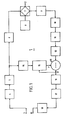
- binary data symbols 3 to be transmitted are initially processed in a scrambler 4 to eliminate auto-correlation in the transmitted data and correlation between data signals transmitted in the two directions of transmission.
- An encoder 5 transforms the binary output data symbols of the scrambler 4 into digital ternary symbols which are transmitted on the line 2 via a transmit filter 6 and a hybrid circuit 7 coupled to a balance circuit 8, the output signals of the transmit filter 6 being analog signals.
- This transmit filter 6 reduces high frequency energy applied to the filter at frequencies higher than half the symbol rate.
- the hybrid circuit 7 is coupled through a filter 9 and a sample and hold circuit 10 in series to an analogue-to-digital converter 11.
- the filter 9 limits the spectrum of the received analog signals to half the symbol rate and the converter 11 converts the sampled signals into a digital form suitable for processing in the rest of the receive path.
- Each received data signal in fact comprises a wanted signal received from the far end and an unwanted signal due to the imperfect operation of the hybrid circuit 7.
- the output data signals of the converter 11 are supplied to one terminal of a subtractor 13 via a digital filter 12.
- the data signals generated at the output of the encoder 5 are supplied to the other terminal of the subtractor 13 through a sample and hold circuit 14 and a digital adaptive echo simulator 15 which is also controlled by the error signal produced at the output D of the subtractor 13.
- This simulator 15 is for instance a digital adaptive transversal filter which adjusts automatically to match the trans-hybrid impulse response, which is the impulse response from the transmit path to the subtractor 13, until the last mentioned error signal from the latter subtractor has substantially no local signal content. It generates an output for each sampled input value from the sample and hold circuit 14.
- the error signal generated at the output D of the subtractor 13 is also applied to an adaptive decision feedback equalizer 16 whose purpose is to detect the received symbol value and to remove intersymbol interference between received symbols due to the transmission on the line.
- the output signal of the equalizer 16 is also applied to a decoder 17 which is in effect the inverse of the encoder 5.
- the output signal of the decoder 17 is applied to a descrambler 18 whose output is the receive signal output 19.
- the adaptive filter 15 is an n+1 tap filter able to calculate the following functions for each time period i during which a periodic input symbol Ti is applied to it with wherein
- the function (1) may be obtained by calculating successively the following partial results or inner products:
- the function (1) may therefore be calculated by means of a so-called systolic processor with n+1 interconnected cells able to calculate respective ones of the inner products P k , i given by the relation (4).
- the functions (2) may be calculated in a similar way in respective cells of a systolic processor because each of them is of the same type as the function (4).
- Each of the functions (2) and (4) may be calculated on a bit parallel or word basis, but in this case a multi-bit multiplier and a multi-bit full adder are required in each cell. Such a multiplier and adder necessitate a relatively large area when integrated on a chip.
- the-filter 15 computes the above functions on a bit serial basis in each cell use may be made, in time multiplex, of a 1-bit multiplier and of a 1-bit adder which can be integrated on a relatively small chip area.
- Such a bit serially operated adaptive transversal filter 15 is described hereinafter by making reference to Fig. 2.
- the filter 15 shown therein is adapted to calculate the filter output signal F according to the relation (3) by successively calculating the inner products P k , l and to use this filter output signal t2m9.6and the above mentioned error signal to calculate the filter coefficients according to the relation (2).
- a clock CL not shown
- delays of p time slots are indicated by z -P , wherein z is the z-operator.
- the digital adaptive transversal filter 15 shown comprises a digital transversal filter circuit proper FC for computing the filter output signal F and a digital filter coefficient updating circuit CUC for calculating the updated filter coefficients for the circuit FC.
- the pairs of interconnected subcells SCO, SC'0 to SC49, SC'49 constitute the cells C ⁇ to C49 of the adaptive filter respectively.
- the input TF is connected to the input TK via a delay unit 20 of 3 symbol periods or 96 time slots as indicated by z -96 . The reason for this delay will be explained later.
- the output F of the filter 15 is connected to an input of the subtractor 13 and the output of this subtractor 13 is connected to the error input E through other circuitry (not shown) giving rise to additional delays and performing a scaling operation.
- the binary point of the filter output signal F for instance occurs in a time slot TS18 the binary point of an error signal Di which appears on error input E and which is a 16- bit signal occurs in a time slot TS4.
- the least significant bit LSB of this signal then occurs in time slot TS25 whilst the most significant bit MSB occurs in time slot TS8.
- Each subcell SC k i.e. SC ⁇ /49, of the filter coefficient updating circuit CUC includes a 1-bit multiplier 21 and a 1-bit adder 22 which together have an inherent delay of one time slot schematically represented by the delay unit 23 clocked by the clock CL and the input of which is connected to the output of the adder 22.
- the output S of the latter delay unit 23 is connected to an input B of this adder 22 via the delay units 24 and 25, clocked by CL, in series.
- the latter delay units 24 and 25 provide a delay equal to 27 and 4 time slots indicated by z -27 and z -4 respectively.
- an updated filter coefficient K k,i produced at the output of the adder 27 of a subcell SC k is delayed by 32 time slots or 1 symbol period before being fed back to the input B of this adder 22, and by 28 time slots before being applied to the input A of the corresponding subcell SC' k .
- the subcell SC k also includes a triggered delay unit 26 of one symbol period indicated by z -32 and a delay unit 27 of one time slot clocked by CL and indicated by z -1 .
- the outputs of the delay units 26 and 27 are connected to respective inputs of the multiplier 21 whose output is connected to an input of the adder 22.
- the triggered delay units 26 of the subcells SCO to SC49 are connected in series between the input symbol terminal TK and the input of multiplier 21 of SC49.
- the delay units 26 of the subcells SC49 to SCO are triggered during the successive time slots TS9 to TS26 respectively, for reasons which will be explained later.
- the delay units 27 of these subcells SC'49 to SCO are connected in series between the error input terminal E and the output terminal EO of subcell SCO.
- Each subcell SC' k i.e. SC'0/49, of the transversal filter proper FC includes a 1-bit multipliere 28 and 1-bit adder 29 which together have an inherent delay of one time slot schematically represented by the delay unit 30 clocked by the clock CL and the input of which is connected to the output of the adder 29.
- the output S of the latter delay unit 30 is connected to an output POUT of the subcell SC' k .
- This subcell SC' k also includes a triggered delay unit 31 of one symbol period indicated by z -32 .
- the outputs of the delay units 31 and 24 are connected to respective inputs of the multiplier 28 whose output is connected to an input of the adder 29.
- the triggered delay units 31 of the subcells SC'0 to SC'49 are connected in series between the symbol input terminal TF and the input of multipler 28 of SC'49.
- the delay units 31 of the subcells SC'49 to SC'0 are also triggered during the successive time slots TS9 to TS26 respectively for reasons which will be explained later.
- the outputs POUT of the subcells SC'49 to SC'1 are connected to the inputs B of the adders 29 of the subcells SC'48 to SC'0 respectively via the PIN inputs of these subcells.
- the PIN input of SC'49 is grounded, as already mentioned.
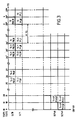
- Fig. 3 shows how the symbols T 1-49 to T 1 are successively entered in the subcells SC'49 to SC'0 during the 50 successive time slots TS9 to TS26'. These symbols are really T 1-49 to T 1 because, as will be explained later, a symbol applied to a subcell is applied 31 time slots later to the immediately following subcell. This is shown in Fig. 3, for the symbol T which is entered in SC'0 in time slot TS26' and in SC'1 in time slot TS25" occurring 31 time slots later.
- the symbol periods in the subcells SC0 to SC49 as well as those in the subcells SC'0 to SC'49 are time shifted by one time slot with respect tp one another.
- the error input signal Di applied to the error input E of subcell SC49 is each time delayed by one time slot in a delay unit 27 before being applied to a following subcell. Because as mentioned above the binary point of the 16-bit error signal Di (Fig. 4) at error input E occurs in TS4, this binary point appears in the subcells SC49 to SCO in the time slots TS4 to TS21 respectively.
- the LSB of this signal occurs in the same subcells SC49 to SCO in the time slots TS25 to TS10 respectively, whereas the MSB occurs in the time slots TS8 to TS25 respectively. Because the input symbols are entered in these subcells in the 50 successive time slots TS9 to TS26 respectively, in each subcell and with respect to the respective symbol period the LSB of the error signal Di is received 16 time slots after the receipt of an input symbol, as is clearly shown in Fig. 4. Thus the bits of the error signal Di can be successively multiplied with this symbol.
- the updated and delayed filter coefficients K49,i to KO,i applied to the multipliers 28 from the subcells SC49 to SCO are shifted by one time slot. More particularly, in the subcells SC'49 to SC'0 the binary points of these coefficients occur in the time slots TS0 to TS17 respectively, whereas their LSB occur in the time slots TS18 to TS3 respectively and their MSB occur in the time slots TS4 to TS31 respectively. Because the input symbols are also entered in these subcells in 50 successive time slots TS9 to TS26 respectively, in each subcell and with respect to the respective symbol period the LSB of the last mentioned output signal is received 9 time slots after the receipt of an input symbol. Thus the bits of each filter coefficient can be successively multiplied with the corresponding input symbol.
- the input symbol T is entered in SC'0 during a time slot TS26, e.g. TS26(0) in Fig. 4, whereas bit K ⁇ ,i, ⁇ of rank 0 of the filter coefficient K ⁇ ,i and bit P 1,i, ⁇ of rank 0 of the inner product P 1,i generated in SC1 are applied to the multiplier 28 and adder 29 in a time slot TS30 (not shown) following TS26(0) respectively.
- the input symbol T is first multiplied in multiplier 28 with bit K ⁇ ,i, ⁇ and the resulting product bit is added to bit iP 1,i, ⁇ to obtain a new bit P ⁇ ,i, ⁇ of rank 0 of the inner product P ⁇ ,i and a possible carry bit which for simplicity reasons is not considered further.
- the error signal at the output D of the subtractor 13 appears as a 16-bit signal Di at the error input D of SC49 of the circuit CUC during time slots TS25 to TS8 (Fig. 4).
- the binary point of this error signal Di occurs 50 time slots after the occurrence of the binary point of the filter output signal F.
- This error signal is further delayed in the 49 delay units 27 and its LSB and MSB are applied to the multiplier 27 of the subcells SC0 in the time slots TS10(4) and TS25(4) respectively. From Fig. 4 it follows that the symbol T is entered in SCO from TS26-3) to TS26(4). All the bits of Di may therefore be correlated with T i .
- the error signal Di may be correlated with the symbols T i-1 , T i-2 , ... , T i-52 in the subcells SC1 to SC49 since in these subcells both the symbol and the error signal have the same relative position as in subcell SCO, as shown in Fig. 4 for SC0 and SC49.
- the correlation product is obtained in SCO by multiplying the input symbol T i in multiplier 21 with the bit of rank 0 of the error signal Di during time slot TS1 ⁇ (4) (Fig. 4).
- This product bit is then added in adder 22 to the bit of rank 0, i.e. K ⁇ ,i-1, ⁇ of the previous filter coefficient K ⁇ ,i-1 to obtain the bit of rank 0, i.e. K ⁇ ,i, ⁇ of the updated filter coefficient K ⁇ ,i and a possible carry bit which is not considered further. Because of the inherent delay of one time slot produced by these operations and represented by delay unit 23 the last mentioned bit is produced in TS11(4).
- the subcells SC'49 to SC'O successively calculate the bits of rank 0 of the inner products P 49 , 49 - 1 to P ⁇ ,i respectively.
- these bits are indicated without the subscript i, i-1, ... etc. in Fig. 3 and in the following. More particularly:
- the bits of other rank of the filter output signal are calculated in the same way. From the above it follows that by calculating each bit during a single time slot and by performing the calculation of bits of a same rank during shifted time slots each such bit can be immediately used for a following calculation in a preceding cell. Hence, the present arrangement operates with a great efficiency. Another advantage is that as a result of this asynchronous operation each symbol has only to be fed to a single cell and not to all cells simultaneously. Thus, there is no danger of introducing unwanted delays between input symbols as is the case when these symbols are fed to all the cells simultaneously and when the number of cells is high.
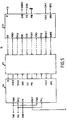
- FIG. 5 showing an adaptve transversal filter circuit 15 similar to that of Fig. 2 and also comprising 50 cells C0 to C49 each having:
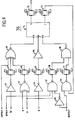
- Fig. 6 represents cell C49 of Fig. 5 in more detail. This cell includes:
- the passing gates 32 and 38 are controlled in a reverse way from terminal SCO directly and through inverter 39.
- the sample and hold units 260 and 261 are controlled from terminal UPD directly and through inverter 40, whilst the sample and hold units 310 and 311 are controlled from the same terminal UPD directly and through inverter 41.
- the delay units 27, 33, 34 and 35 are of the type shown in Fig. 7; the sample and hold units 260, 261, 31 and 311 are of the type represented in Fig. 8 and the delay units 24 and 25 are constituted by 27 and 4 series connected delay units of Fig. 7 respectively. Finally, the processing circuits 36 and 37 are of the type shown in Fig. 9.
- Inverter circuit 48 comprises PMOS transistors 44 and 45 and NMOS transistors 46 and 47 which are all connected in series between V+ and ground.
- the input terminal IN of the unit is connected to the gate electrodes of transistors 44 and 47 and the gate electrodes of transistors 45 and 46 are controlled by CL1 and CL1 respectively.
- the interconnected electrodes of the transistors 45 and 46 are connected to an intermediate output terminal OUT1 and to the input of the inverter 43 which includes the transistors 48 to 51 all connected in a similar way as the transistors 44 to 47 and having output terminal OUT.
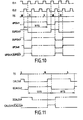
- the delay unit 35 operates as follows when a control pulse waveform such as UPD49 (Fig. 10), which is UPD for C49, is applied to its input IN, this pulse waveform having a period of 32 time slots with a positively directed pulse of 31 time slots and a single negatively directed pulse of one time slot:
- Fig. 10 also shows the pulse waveform UPD49.DUPD49.
- Fig. 11 shows the pulse waveform CALC49.DCALC49.
- the sample and hold unit 260 of cell C49 which is similar to the units 261, 310 and 311 is shown in Fig. 8. It has an input terminal IN which is connected to its output terminal OUT via the series connection of passing gates 52 and 53, inverter 54, passing gate 55 and inverter 56 in series.
- the passing gates 52 and 55 are controlled from terminals UPD and UPD controlled by the above mentioned pulse waveform UPD49 and the inverse UPD49 thereof respectively, whilst passing gate 53 is controlled by clock pulses CL1 and CL1.
- the output OUT is also coupled back to the junction point of passing gates 52 and 53 via passing gate 57 which is also controlled by the pulse waveforms UPD49 and UPD49.
- the sample and hold unit 260 of cell C49 operates as follows, it being supposed that a symbol is stored in the output capacitance of the inverter 56 of the circuit 260 of cell C48 since the de-activation (binary 0) of the pulse waveform UPD48 in the course of TS10. This symbol remains at this output for 32 time slots i.e. until the start of CL2 in the following TS10:
- the delay of 31 time slots is realized in a particularly simple way by the use of a single pulse waveform UPD49 which is successively delayed by one time slot in the cells C49 to C0 to provide the successive corresponding symbol entering time slots TS9 to TS26 respectively.
- the processing circuit 36 represented in Fig. 9 has input terminals A, B, T0, T1, UPD, DUPD and EUPD and output terminal S. It includes a combinatorial logic circuit with NAND gates 58 to 60, NOR gate 61, Exclusive-NOR gate 62, inverters 63 and 66, passing gates 67 to 73 and a well known adder circuit 74 having inputs Q, R, T, sum output S and carry output C.
- the passing gate 67 to 71 are controlled by clock pulses CL1 and CL1
- the passing gates 72 and 73 are controlled by clock pulses CL2 and CL2.
- the signals Q, R and T applied to adder circuit 74 may be represented by the Boolean functions wherein A, B, T0, T1, EUPD49 and DUPD49 are the signals applied, together with UPD49, to the like named inputs of circuit 36 and C is the carry signal generated at the carry output C of the processing circuit 36.
- the sum signal S appearing at the sum output S of the adder 74 is applied to the output S of circuit 36 via passing gate 72 clocked by CL2 and CL2, whilst the carry signal C provided at the carry output C of this adder 74 is fed back to an input of the NAND-gate 59, to be used during a following calculation, via passing gate 73 also clocked by CL2 and CL2.
- the processing circuit 37 is identical to processing circuit 36 but is controlled by the above mentioned pulse waveforms CALC, ECALC and DCALC.
- the signals applied to the adder circuit 74 of circuit 37 are obtained by substituting the signals CALC, ECALC and DCALC for UPD, EUPD and DUPD in the relations (7), (8) and (9).
- the pulse waveform UPD49 (Fig. 10) is applied to input terminal UPD of cell C49 (Fig. 6) whose input terminal PIN is grounded. Its successive edges occur in time slots TS9 and TS10 in coincidence with clock pulses CL2.
- the pulse waveform CALC49 (Fig. 11) is applied to input terminal CALC of cell C49. Its successive edges occur in time slots TS5 and TS18.
- the pulse waveforms UPD49 and CALC49 are applied to delay circuits 35 and 34 at the outputs of which appear the pulse waveforms EUPD49, DUPD49 and ECALC49, DCALC49 respectively. These pulse waveforms are applied to the corresponding input terminals of the processing circuits 36 and 37 to which also the pulse waveforms UPD49 and CALC49 are applied.
- the above mentioned error signal Di is applied to the input terminal A upon the occurrence of clock pulse CL2 of TS25 (Fig. 4) and the same is true for the filter coefficient calculated during a previous symbol period and applied to input terminal B of the processing circuit 36.
- the clock pulse CL1 at the start of time slot TS11 the signals at the terminals T0, T1, A, B, UPD and the carry bit C are entered in the processing circuit 36.
- the signal EUPD49 is de-activated from the start of TS11 the signal applied to the adder input Q of the adder circuit 74 is then equal to A, 0 or A.
- the signal applied to the adder input R is equal to that applied to terminal B of the processing circuit 76.
- the first bit of the calculated filter coefficient appears at the output S of the processing circuit 36 during time slot TS11.
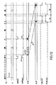
- the following bits 1 to 30 are generated in the same way during the successive time slots TS11 to TS9 (Fig. 12), no bit 31 being generated because EUPD49 is then activated (Fig. 11).
- the bits of the 31-bit filter coefficient thus obtained are applied to the delay unit 24 via passing gate 38 which is supposed to be closed because terminal SCO is de-activated.
- these bits are delayed by 27 time slots so that they appear at the input A of the processing circuit 36 during the 31 successive time slots TS6 to TS4 as shown in Fig. 12.
- These bits are also fed back to the input B of the circuit 36 via the gate 38 and delay units 24 and 25 in series in order to be used during a subsequent operation.
- the signals applied to the inputs A, B, T0, T1, CALC, ECALC, DCALC are processed in the same way as described for processing circuit 36.
- the control signal ECALC49 being de-activated for 19 time slots TS18 to TS4 the filter coefficient generated has only 19 bits, as shown in Fig. 12.
- the resultant filter output bits appearing at the output S of the circuit 37 are successively applied to the output terminal POUT and from there to the input terminal PIN of the cell C48 (not shown). Therein they are each used during the following time slot to calculate another filter output as already explained in relation to Figs. 2 and 4.
- the cell C48 also receives the error signal Di after the latter has been delayed by one time slot in delay unit 27, as well as the signals DUPD and DCALC.
- gate 38 was supposed to be closed due to the input SCIN of C49 being de-activated. In this case gate 32 of C49 was open. To reverse this situation it is sufficient to activate this input. This may for instance be required when the updated filter coefficients K 49,i to K ⁇ ,i have to be read out one after another.
- coefficients K 49 , 1 to K ⁇ ,i are 31-bit words the bits of which are successively generated at the outputs S of the units 36 of the cells C49 to C0 with a time shift of one time slot. To read out the complete coefficients one after another, it is sufficient to apply an activated pulse waveform to the above input SCIN after the coefficient K 49 , 1 has been completely entered into the delay units 24 and 25 of C49 and start the shifting out operation.
Landscapes
- Engineering & Computer Science (AREA)
- Computer Networks & Wireless Communication (AREA)
- Signal Processing (AREA)
- Filters That Use Time-Delay Elements (AREA)
- Cable Transmission Systems, Equalization Of Radio And Reduction Of Echo (AREA)
- Complex Calculations (AREA)
Claims (14)





Priority Applications (6)
| Application Number | Priority Date | Filing Date | Title |
|---|---|---|---|
| EP84201049A EP0167677B1 (de) | 1984-07-13 | 1984-07-13 | Anordnung zur Signalverarbeitung |
| US06/749,354 US4803648A (en) | 1984-07-12 | 1985-06-27 | Echo canceller using an adaptive finite impulse response filter |
| AU44273/85A AU577127B2 (en) | 1984-07-12 | 1985-06-28 | Digital signal processor |
| JP60153899A JPS6145622A (ja) | 1984-07-13 | 1985-07-12 | 信号処理装置 |
| ES85545163A ES8701439A1 (es) | 1984-07-13 | 1985-07-12 | Una configuracion de un procesador de senal |
| BE2/60746A BE902895A (nl) | 1984-07-13 | 1985-07-15 | Signaalverwerkingseenheid |
Applications Claiming Priority (1)
| Application Number | Priority Date | Filing Date | Title |
|---|---|---|---|
| EP84201049A EP0167677B1 (de) | 1984-07-13 | 1984-07-13 | Anordnung zur Signalverarbeitung |
Publications (2)
| Publication Number | Publication Date |
|---|---|
| EP0167677A1 EP0167677A1 (de) | 1986-01-15 |
| EP0167677B1 true EP0167677B1 (de) | 1989-03-08 |
Family
ID=8192460
Family Applications (1)
| Application Number | Title | Priority Date | Filing Date |
|---|---|---|---|
| EP84201049A Expired EP0167677B1 (de) | 1984-07-12 | 1984-07-13 | Anordnung zur Signalverarbeitung |
Country Status (6)
| Country | Link |
|---|---|
| US (1) | US4803648A (de) |
| EP (1) | EP0167677B1 (de) |
| JP (1) | JPS6145622A (de) |
| AU (1) | AU577127B2 (de) |
| BE (1) | BE902895A (de) |
| ES (1) | ES8701439A1 (de) |
Families Citing this family (8)
| Publication number | Priority date | Publication date | Assignee | Title |
|---|---|---|---|---|
| US4982354A (en) * | 1987-05-28 | 1991-01-01 | Mitsubishi Denki Kabushiki Kaisha | Digital finite impulse response filter and method |
| GB8719307D0 (en) * | 1987-08-14 | 1987-09-23 | Gen Electric Co Plc | Echo canceller |
| US5386472A (en) * | 1990-08-10 | 1995-01-31 | General Motors Corporation | Active noise control system |
| JPH08125591A (ja) * | 1994-10-20 | 1996-05-17 | Fujitsu Ltd | エコーキャンセラシステム |
| US6430287B1 (en) | 1997-03-25 | 2002-08-06 | Level One Communications, Inc. | Combined parallel adaptive equalizer/echo canceller |
| US20020021693A1 (en) * | 1998-05-01 | 2002-02-21 | At&T Corp. | Sharing of voice-switched network and internet resources for intelligent session processing |
| US6563802B2 (en) * | 1998-06-22 | 2003-05-13 | Intel Corporation | Echo cancellation with dynamic latency adjustment |
| KR102883344B1 (ko) | 2020-07-31 | 2025-11-07 | 삼성전자주식회사 | 딥러닝 연산 수행 방법 및 장치 |
Family Cites Families (18)
| Publication number | Priority date | Publication date | Assignee | Title |
|---|---|---|---|---|
| FR2272544B1 (de) * | 1974-05-24 | 1977-03-11 | Cit Alcatel | |
| US4369499A (en) * | 1980-09-18 | 1983-01-18 | Codex Corporation | Linear phase digital filter |
| US4386430A (en) * | 1980-10-23 | 1983-05-31 | International Telephone And Telegraph Corporation | Automatic equalizer for synthesizing recursive filters |
| US4425483A (en) * | 1981-10-13 | 1984-01-10 | Northern Telecom Limited | Echo cancellation using transversal filters |
| GB2111354B (en) * | 1981-11-19 | 1985-06-19 | Standard Telephones Cables Ltd | Echo canceller |
| US4493048A (en) * | 1982-02-26 | 1985-01-08 | Carnegie-Mellon University | Systolic array apparatuses for matrix computations |
| EP0090904B1 (de) * | 1982-04-03 | 1985-08-21 | Deutsche ITT Industries GmbH | Schaltungsanordnung für seriell arbeitende Digitalfilter |
| FR2528643A1 (fr) * | 1982-06-14 | 1983-12-16 | Trt Telecom Radio Electr | Procede destine a reduire le temps de convergence d'un annuleur d'echo et dispositif utilise pour mettre en oeuvre ce procede |
| US4588255A (en) * | 1982-06-21 | 1986-05-13 | The Board Of Trustees Of The Leland Stanford Junior University | Optical guided wave signal processor for matrix-vector multiplication and filtering |
| US4507725A (en) * | 1982-07-01 | 1985-03-26 | Rca Corporation | Digital filter overflow sensor |
| US4582963A (en) * | 1982-07-29 | 1986-04-15 | Rockwell International Corporation | Echo cancelling using adaptive bulk delay and filter |
| US4621172A (en) * | 1982-12-22 | 1986-11-04 | Nec Corporation | Fast convergence method and system for echo canceller |
| FR2540314A1 (fr) * | 1983-01-31 | 1984-08-03 | Trt Telecom Radio Electr | Procede d'initialisation des coefficients de filtres dans un dispositif d'annulation d'echos proche et lointain et dispositif de mise en oeuvre de ce procede |
| US4574166A (en) * | 1983-02-04 | 1986-03-04 | At&T Bell Laboratories | Tandem adaptive filter arrangement |
| FR2541837A1 (fr) * | 1983-02-25 | 1984-08-31 | Trt Telecom Radio Electr | Procede de reduction du temps de convergence d'un annuleur d'echo et dispositif pour mettre en oeuvre ce procede |
| US4591669A (en) * | 1984-09-26 | 1986-05-27 | At&T Bell Laboratories | Adaptive filter update gain normalization |
| US4773034A (en) * | 1985-05-09 | 1988-09-20 | American Telephone And Telegraph Company | Adaptive equalizer utilizing a plurality of multiplier-accumulator devices |
| US4683496A (en) * | 1985-08-23 | 1987-07-28 | The Analytic Sciences Corporation | System for and method of enhancing images using multiband information |
-
1984
- 1984-07-13 EP EP84201049A patent/EP0167677B1/de not_active Expired
-
1985
- 1985-06-27 US US06/749,354 patent/US4803648A/en not_active Expired - Lifetime
- 1985-06-28 AU AU44273/85A patent/AU577127B2/en not_active Ceased
- 1985-07-12 JP JP60153899A patent/JPS6145622A/ja active Pending
- 1985-07-12 ES ES85545163A patent/ES8701439A1/es not_active Expired
- 1985-07-15 BE BE2/60746A patent/BE902895A/nl not_active IP Right Cessation
Also Published As
| Publication number | Publication date |
|---|---|
| US4803648A (en) | 1989-02-07 |
| AU4427385A (en) | 1986-01-16 |
| EP0167677A1 (de) | 1986-01-15 |
| AU577127B2 (en) | 1988-09-15 |
| ES545163A0 (es) | 1986-10-01 |
| JPS6145622A (ja) | 1986-03-05 |
| BE902895A (nl) | 1986-01-15 |
| ES8701439A1 (es) | 1986-10-01 |
Similar Documents
| Publication | Publication Date | Title |
|---|---|---|
| US4038536A (en) | Adaptive recursive least mean square error filter | |
| Clark et al. | Block implementation of adaptive digital filters | |
| US6009448A (en) | Pipelined parallel-serial architecture for a modified least mean square adaptive filter | |
| KR100281254B1 (ko) | 비동기 cdma 시스템용 데이타 복원 장치 및 방법 | |
| EP0023056A1 (de) | Vorrichtung mit einem nichtrekursiven Filter | |
| EP1525537A2 (de) | Verfahren zur lösung linearer gleichungssysteme, insbesondere in kommunikationssystemen | |
| US6279020B1 (en) | Programmable circuit for realizing a digital filter | |
| EP0373468B1 (de) | Pipelineprozessor zur Durchführung des LMS Algorithmus | |
| US4803648A (en) | Echo canceller using an adaptive finite impulse response filter | |
| US5001661A (en) | Data processor with combined adaptive LMS and general multiplication functions | |
| US4785411A (en) | Cascade filter structure with time overlapped partial addition operations and programmable tap length | |
| Chandekar et al. | Delay and power optimized adaptive filter using distributed arithmetic | |
| Chakraborty et al. | A trigonometric formulation of the LMS algorithm for realization on pipelined CORDIC | |
| Wyrzykowski et al. | Flexible systolic architecture for VLSI FIR filters | |
| Lawrence et al. | Multiprocessor implementation of adaptive digital filters | |
| US5907497A (en) | Update block for an adaptive equalizer filter configuration | |
| WO1988007790A1 (en) | Digital adaptive filter | |
| GB2225883A (en) | Method of determining the tap weights of a decision feedback equaliser | |
| US5233549A (en) | Reduced quantization error FIR filter | |
| Tiwari et al. | High throughput adaptive block FIR filter using distributed arithmetic | |
| Mankar et al. | Design and Verification of low power DA-Adaptive digital FIR filter | |
| Harada et al. | Pipelined architecture of the LMS adaptive digital filter with the minimum output latency | |
| GB2102255A (en) | Two-wire line for digital communication | |
| JP2888121B2 (ja) | 適応フィルタによる未知システム同定の方法及び装置 | |
| Coleman | Cascaded coefficient number systems lead to FIR filters of striking computational efficiency |
Legal Events
| Date | Code | Title | Description |
|---|---|---|---|
| PUAI | Public reference made under article 153(3) epc to a published international application that has entered the european phase |
Free format text: ORIGINAL CODE: 0009012 |
|
| AK | Designated contracting states |
Designated state(s): AT BE CH DE FR GB IT LI LU NL SE |
|
| RBV | Designated contracting states (corrected) |
Designated state(s): FR GB IT NL |
|
| 17P | Request for examination filed |
Effective date: 19860704 |
|
| RAP1 | Party data changed (applicant data changed or rights of an application transferred) |
Owner name: BELL TELEPHONE MANUFACTURING COMPANY NAAMLOZE VENN Owner name: ALCATEL N.V. |
|
| 17Q | First examination report despatched |
Effective date: 19871124 |
|
| RAP3 | Party data changed (applicant data changed or rights of an application transferred) |
Owner name: ALCATEL N.V. Owner name: BELL TELEPHONE MANUFACTURING COMPANY NAAMLOZE VENN |
|
| RAP1 | Party data changed (applicant data changed or rights of an application transferred) |
Owner name: ALCATEL N.V. Owner name: BELL TELEPHONE MANUFACTURING COMPANY NAAMLOZE VENN |
|
| GRAA | (expected) grant |
Free format text: ORIGINAL CODE: 0009210 |
|
| ITF | It: translation for a ep patent filed | ||
| AK | Designated contracting states |
Kind code of ref document: B1 Designated state(s): FR GB IT NL |
|
| ET | Fr: translation filed | ||
| PLBE | No opposition filed within time limit |
Free format text: ORIGINAL CODE: 0009261 |
|
| STAA | Information on the status of an ep patent application or granted ep patent |
Free format text: STATUS: NO OPPOSITION FILED WITHIN TIME LIMIT |
|
| 26N | No opposition filed | ||
| ITTA | It: last paid annual fee | ||
| NLS | Nl: assignments of ep-patents |
Owner name: ALCATEL N.V. TE AMSTERDAM. |
|
| PGFP | Annual fee paid to national office [announced via postgrant information from national office to epo] |
Ref country code: GB Payment date: 19980612 Year of fee payment: 15 |
|
| PGFP | Annual fee paid to national office [announced via postgrant information from national office to epo] |
Ref country code: NL Payment date: 19980629 Year of fee payment: 15 |
|
| PG25 | Lapsed in a contracting state [announced via postgrant information from national office to epo] |
Ref country code: GB Free format text: LAPSE BECAUSE OF NON-PAYMENT OF DUE FEES Effective date: 19990713 |
|
| PG25 | Lapsed in a contracting state [announced via postgrant information from national office to epo] |
Ref country code: NL Free format text: LAPSE BECAUSE OF NON-PAYMENT OF DUE FEES Effective date: 20000201 |
|
| GBPC | Gb: european patent ceased through non-payment of renewal fee |
Effective date: 19990713 |
|
| NLV4 | Nl: lapsed or anulled due to non-payment of the annual fee |
Effective date: 20000201 |
|
| PGFP | Annual fee paid to national office [announced via postgrant information from national office to epo] |
Ref country code: FR Payment date: 20030711 Year of fee payment: 20 |