EP0167732A1 - Procédé pour la fabrication d'un matériau de base pour un circuit hybride - Google Patents
Procédé pour la fabrication d'un matériau de base pour un circuit hybride Download PDFInfo
- Publication number
- EP0167732A1 EP0167732A1 EP85104961A EP85104961A EP0167732A1 EP 0167732 A1 EP0167732 A1 EP 0167732A1 EP 85104961 A EP85104961 A EP 85104961A EP 85104961 A EP85104961 A EP 85104961A EP 0167732 A1 EP0167732 A1 EP 0167732A1
- Authority
- EP
- European Patent Office
- Prior art keywords
- conductor tracks
- metal layer
- contact points
- insulating layer
- substrate
- Prior art date
- Legal status (The legal status is an assumption and is not a legal conclusion. Google has not performed a legal analysis and makes no representation as to the accuracy of the status listed.)
- Granted
Links
Images
Classifications
-
- H—ELECTRICITY
- H10—SEMICONDUCTOR DEVICES; ELECTRIC SOLID-STATE DEVICES NOT OTHERWISE PROVIDED FOR
- H10W—GENERIC PACKAGES, INTERCONNECTIONS, CONNECTORS OR OTHER CONSTRUCTIONAL DETAILS OF DEVICES COVERED BY CLASS H10
- H10W70/00—Package substrates; Interposers; Redistribution layers [RDL]
- H10W70/60—Insulating or insulated package substrates; Interposers; Redistribution layers
- H10W70/611—Insulating or insulated package substrates; Interposers; Redistribution layers for connecting multiple chips together
-
- H—ELECTRICITY
- H10—SEMICONDUCTOR DEVICES; ELECTRIC SOLID-STATE DEVICES NOT OTHERWISE PROVIDED FOR
- H10W—GENERIC PACKAGES, INTERCONNECTIONS, CONNECTORS OR OTHER CONSTRUCTIONAL DETAILS OF DEVICES COVERED BY CLASS H10
- H10W70/00—Package substrates; Interposers; Redistribution layers [RDL]
- H10W70/01—Manufacture or treatment
- H10W70/05—Manufacture or treatment of insulating or insulated package substrates, or of interposers, or of redistribution layers
-
- H—ELECTRICITY
- H10—SEMICONDUCTOR DEVICES; ELECTRIC SOLID-STATE DEVICES NOT OTHERWISE PROVIDED FOR
- H10W—GENERIC PACKAGES, INTERCONNECTIONS, CONNECTORS OR OTHER CONSTRUCTIONAL DETAILS OF DEVICES COVERED BY CLASS H10
- H10W70/00—Package substrates; Interposers; Redistribution layers [RDL]
- H10W70/60—Insulating or insulated package substrates; Interposers; Redistribution layers
- H10W70/62—Insulating or insulated package substrates; Interposers; Redistribution layers characterised by their interconnections
- H10W70/641—Adaptable interconnections, e.g. fuses or antifuses
-
- H—ELECTRICITY
- H05—ELECTRIC TECHNIQUES NOT OTHERWISE PROVIDED FOR
- H05K—PRINTED CIRCUITS; CASINGS OR CONSTRUCTIONAL DETAILS OF ELECTRIC APPARATUS; MANUFACTURE OF ASSEMBLAGES OF ELECTRICAL COMPONENTS
- H05K1/00—Printed circuits
- H05K1/02—Details
- H05K1/0286—Programmable, customizable or modifiable circuits
Definitions
- the invention relates to a method for producing a base material for a hybrid circuit, consisting of a carrier substrate with multilayer metal layers which are electrically insulated from one another and can be subdivided in each case by suitable means into chip contact areas and conductor tracks.
- the invention is therefore based on the object of providing a hybrid base material which can be used universally and by means of which individual electrical circuits are possible in an economical manner, with minimal modifications, while maintaining the highest possible packing density.
- This object is achieved according to the invention in that the number of first conductor tracks formed from the one metal layer and the number of second conductor tracks formed from the other metal layer are specified at program-like contact points of the in different levels arranged and intersecting interconnects can be contacted with suitable means for forming an electrical circuit.
- the programmable hybrid substrate according to the invention can be produced using the methods and techniques known per se and stored as a base material, as a result of which the high one-off costs for circuit-specific design work and tools are eliminated. Another advantage is that this hybrid substrate ensures a high packing density and thus short connecting conductors, thereby permitting a high signal processing speed. Another advantage is seen in the fact that the programmability of the hybrid substrate enables a variety of circuits to be implemented which are almost copy-proof due to the always identical layout of the surface structure.
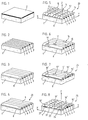
- FIG. 1, 1 denotes an electrically insulating substrate provided as a carrier element, on which a first metal layer 2 is vapor-deposited or sputtered.
- the metal layer 2 is etched in accordance with the photolithographic method of semiconductor technology known per se in such a way that, as shown in FIG. 2, a first group of conductor tracks 3, 4, 5, 6, 6 and 7 is formed parallel to one another.
- a first insulating layer shown in FIG. 3 and designated 8 is applied to the first conductor track group 3 to 7.
- This first insulating layer 8 serves as a protective layer electrically insulating the conductor tracks 3 to 7, to which, as shown in FIG. 4, a second metal layer 9 is applied.
- the second metal layer 9 is etched in such a way that a second group of conductor tracks 10, 11, 12 and 13 is arranged parallel to one another.
- the conductor tracks 10 to 13 are oriented essentially transversely to the conductor tracks 3 to 7 etched from the first metal layer 2.
- contact points K are formed which are electrically insulated from one another by the first insulating layer 8.
- FIG. 5 only one group of contact points K is designated for a better overview.
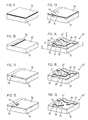
- the insulating layer 8 consists of polycrystalline, highly insulating silicon and the first and second metal layers 2, 9 for the upper and lower conductor tracks 3 to 7 and 10 to 13 consist of the aluminum usually used in semiconductor technology. Taking these features into account, there is the possibility of producing an electrically optimally conductive aluminum-silicon alloy by means of a focused laser beam by locally heating the contact points K to be contacted.
- any type of program is to be applied before the second metal layer is applied predetermined locations from the first insulating layer 8, as shown in more detail in FIG. 6, are etched out correspondingly designed windows 15, 16, 17 and 18.
- the second metal layer 9 ' is applied to the first insulating layer 8 provided with the windows 15 to 18, so that in the region of the windows 15 to 18 between the conductor tracks 3 to 7 and the second insulating layer 9' electrical contact points 15 'to 18' arise.
- the same is etched in such a way that, as shown in FIG.
- the carrier element (FIG. 3) formed from the essential elements 1 to 9 ' serves as the base material and is only after the relevant determination of the contact points 15' essentially formed by the windows 15 to 18. to 18 'and the production of a corresponding etching mask (not shown) for the hybrid substrate designated 25 in its entirety in FIG.
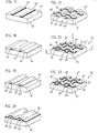
- the first metal layer 32 is etched such that, as shown in FIG. 10, at least one conductor track 33 is formed.
- a first insulating layer 34 (FIG. 11) is now applied to the conductor track 33 and to the surface 31 ′ of the substrate 31.
- At least one window 35 is etched from the insulating layer 34 (FIG. 12) and then, as shown in FIG. 13, a second one on the elements 31, 33, 34 and 35 Metal layer 36 applied. In this case, a contact point 35 ′ is formed in the area of the window 35 between the conductor track 33 and the second metal layer 36.
- the hybrid substrate designated 40 in its entirety in FIG. 14 serves as the prefabricated base material.
- the final state of the hybrid substrate, designated 40 'or 40 " is achieved in such a way that, for example, webs 39 which are not required and which essentially connect the conductor tracks 37 and 38 oriented parallel to one another, according to FIG. 15 by laser, or as shown in Fig. 16, interrupted by etching or removed.
- the first metal layer 32 is etched in this example in such a way that, as shown in FIG. 17, two conductor tracks 33, 33 arranged parallel to one another 'arise.
- a subsequently applied first photoresist layer 44 (FIG. 18), as shown in FIG. 19, is subdivided into individual photoresist bridge parts 44 ′ that electrically isolate the two conductor tracks 33, 33 ′.
- a second metal layer 46 contacting the two bridge parts 44 'and the surface 31' is applied to the bridge parts 44 'and to the surface 31' of the substrate 31, which metal layer 46 is subsequently separated into individual Conductors 47, 48 oriented transversely to the conductor tracks 33, 33 'are subdivided (FIG. 21).
- the bridge parts 44 ′ formed from the photoresist layer 44 are removed by means of suitable means, so that, as shown in FIG. 22, a space 49, 49 ′ is created between the individual conductor tracks 33, 33 ′ and 47, 48.
- the hybrid substrate designated 50 in its entirety in FIG. 22 also serves as a prefabricated base material.
- the final state of the hybrid substrate 50 is essentially achieved by making an electrical contact at predetermined, programmed contact points K "of the intersecting conductor tracks 33, 33 'and 47, 48 and then an electrically insulating protective layer on the hybrid substrate 50 ( The interstices 49 and 49 'of the crossing conductor tracks 33, 33' and 47, 48 which are not designed as contact points K "are electrically insulated from one another.
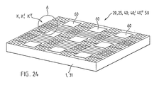
- FIG. 24 A perspective view of a larger section of the hybrid base material labeled 20, 25, 40, 40 ', 40 "and 50 is shown in FIG. 24 and the substrate 1 or 31 and the chip contact area labeled 60 can be seen.
- the one designated by a circle Position A corresponds to that here matically represented contact points K, K ', K "of the intersecting interconnects as described in more detail with reference to Examples I, II, III and IV.
- the hybrid base material 20, 25, 40, 40 ', 40 "and 50 according to the invention, described above and shown essentially as a partial section on a larger scale in FIGS. 1 to 24, can be produced by means of the already known and well-established techniques and processes.
Landscapes
- Internal Circuitry In Semiconductor Integrated Circuit Devices (AREA)
- Paper (AREA)
- Polymers With Sulfur, Phosphorus Or Metals In The Main Chain (AREA)
- Insulated Metal Substrates For Printed Circuits (AREA)
Priority Applications (1)
| Application Number | Priority Date | Filing Date | Title |
|---|---|---|---|
| AT85104961T ATE56310T1 (de) | 1984-06-27 | 1985-04-24 | Verfahren zur herstellung eines basismaterials fuer eine hybridschaltung. |
Applications Claiming Priority (2)
| Application Number | Priority Date | Filing Date | Title |
|---|---|---|---|
| CH310484 | 1984-06-27 | ||
| CH3104/84 | 1984-06-27 |
Publications (2)
| Publication Number | Publication Date |
|---|---|
| EP0167732A1 true EP0167732A1 (fr) | 1986-01-15 |
| EP0167732B1 EP0167732B1 (fr) | 1990-09-05 |
Family
ID=4248699
Family Applications (1)
| Application Number | Title | Priority Date | Filing Date |
|---|---|---|---|
| EP85104961A Expired - Lifetime EP0167732B1 (fr) | 1984-06-27 | 1985-04-24 | Procédé pour la fabrication d'un matériau de base pour un circuit hybride |
Country Status (3)
| Country | Link |
|---|---|
| EP (1) | EP0167732B1 (fr) |
| AT (1) | ATE56310T1 (fr) |
| DE (1) | DE3579515D1 (fr) |
Cited By (12)
| Publication number | Priority date | Publication date | Assignee | Title |
|---|---|---|---|---|
| EP0256494A3 (en) * | 1986-08-12 | 1988-07-27 | Fujitsu Limited | Activatable conductive links for semiconductor devices |
| EP0268971A3 (en) * | 1986-11-24 | 1988-08-17 | Microelectronics & Computer | Electrical interconnect support system with low dielectric constant |
| EP0231970A3 (en) * | 1986-01-31 | 1989-12-27 | Philips Patentverwaltung Gmbh | Thick-film wiring on a ceramic substrate plate |
| EP0329018A3 (fr) * | 1988-02-19 | 1990-02-28 | Microelectronics and Computer Technology Corporation | Circuit adapté à l'usager |
| FR2653595A1 (fr) * | 1989-10-25 | 1991-04-26 | Valtronic France | Circuit electronique a grille d'interconnexion. |
| US5074037A (en) * | 1989-12-01 | 1991-12-24 | Oerlikon-Contraves Ag | Process for producing electrical connections on a universal substrate |
| US5081561A (en) * | 1988-02-19 | 1992-01-14 | Microelectronics And Computer Technology Corporation | Customizable circuitry |
| US5132878A (en) * | 1987-09-29 | 1992-07-21 | Microelectronics And Computer Technology Corporation | Customizable circuitry |
| US5165166A (en) * | 1987-09-29 | 1992-11-24 | Microelectronics And Computer Technology Corporation | Method of making a customizable circuitry |
| EP0619935A4 (fr) * | 1991-12-31 | 1995-03-22 | Tessera Inc | Procedes de construction de circuits multicouche, structures personnalisees et composants utilises dans ce procede. |
| US5558928A (en) * | 1991-12-31 | 1996-09-24 | Tessera, Inc. | Multi-layer circuit structures, methods of making same and components for use therein |
| US5570504A (en) * | 1991-12-31 | 1996-11-05 | Tessera, Inc. | Multi-Layer circuit construction method and structure |
Citations (3)
| Publication number | Priority date | Publication date | Assignee | Title |
|---|---|---|---|---|
| US3525617A (en) * | 1965-07-13 | 1970-08-25 | Int Computers & Tabulators Ltd | Method of making electrical circuit structure for electrical connections between components |
| US3846166A (en) * | 1971-09-25 | 1974-11-05 | Hitachi Ltd | Method of producing multilayer wiring structure of integrated circuit |
| EP0006810A1 (fr) * | 1978-06-29 | 1980-01-09 | L.C.C.-C.I.C.E. - Compagnie Europeenne De Composants Electroniques | Procédé de fabrication d'un circuit intégré hybride |
-
1985
- 1985-04-24 AT AT85104961T patent/ATE56310T1/de not_active IP Right Cessation
- 1985-04-24 EP EP85104961A patent/EP0167732B1/fr not_active Expired - Lifetime
- 1985-04-24 DE DE8585104961T patent/DE3579515D1/de not_active Expired - Lifetime
Patent Citations (3)
| Publication number | Priority date | Publication date | Assignee | Title |
|---|---|---|---|---|
| US3525617A (en) * | 1965-07-13 | 1970-08-25 | Int Computers & Tabulators Ltd | Method of making electrical circuit structure for electrical connections between components |
| US3846166A (en) * | 1971-09-25 | 1974-11-05 | Hitachi Ltd | Method of producing multilayer wiring structure of integrated circuit |
| EP0006810A1 (fr) * | 1978-06-29 | 1980-01-09 | L.C.C.-C.I.C.E. - Compagnie Europeenne De Composants Electroniques | Procédé de fabrication d'un circuit intégré hybride |
Cited By (15)
| Publication number | Priority date | Publication date | Assignee | Title |
|---|---|---|---|---|
| EP0231970A3 (en) * | 1986-01-31 | 1989-12-27 | Philips Patentverwaltung Gmbh | Thick-film wiring on a ceramic substrate plate |
| EP0256494A3 (en) * | 1986-08-12 | 1988-07-27 | Fujitsu Limited | Activatable conductive links for semiconductor devices |
| US4968643A (en) * | 1986-08-12 | 1990-11-06 | Fujitsu Limited | Method for fabricating an activatable conducting link for metallic conductive wiring in a semiconductor device |
| EP0268971A3 (en) * | 1986-11-24 | 1988-08-17 | Microelectronics & Computer | Electrical interconnect support system with low dielectric constant |
| US5132878A (en) * | 1987-09-29 | 1992-07-21 | Microelectronics And Computer Technology Corporation | Customizable circuitry |
| US5438166A (en) * | 1987-09-29 | 1995-08-01 | Microelectronics And Computer Technology Corporation | Customizable circuitry |
| US5165166A (en) * | 1987-09-29 | 1992-11-24 | Microelectronics And Computer Technology Corporation | Method of making a customizable circuitry |
| EP0329018A3 (fr) * | 1988-02-19 | 1990-02-28 | Microelectronics and Computer Technology Corporation | Circuit adapté à l'usager |
| US5081561A (en) * | 1988-02-19 | 1992-01-14 | Microelectronics And Computer Technology Corporation | Customizable circuitry |
| FR2653595A1 (fr) * | 1989-10-25 | 1991-04-26 | Valtronic France | Circuit electronique a grille d'interconnexion. |
| US5074037A (en) * | 1989-12-01 | 1991-12-24 | Oerlikon-Contraves Ag | Process for producing electrical connections on a universal substrate |
| EP0619935A4 (fr) * | 1991-12-31 | 1995-03-22 | Tessera Inc | Procedes de construction de circuits multicouche, structures personnalisees et composants utilises dans ce procede. |
| US5558928A (en) * | 1991-12-31 | 1996-09-24 | Tessera, Inc. | Multi-layer circuit structures, methods of making same and components for use therein |
| US5570504A (en) * | 1991-12-31 | 1996-11-05 | Tessera, Inc. | Multi-Layer circuit construction method and structure |
| US5583321A (en) * | 1991-12-31 | 1996-12-10 | Tessera, Inc. | Multi-layer circuit construction methods and structures with customization features and components for use therein |
Also Published As
| Publication number | Publication date |
|---|---|
| ATE56310T1 (de) | 1990-09-15 |
| EP0167732B1 (fr) | 1990-09-05 |
| DE3579515D1 (de) | 1990-10-11 |
Similar Documents
| Publication | Publication Date | Title |
|---|---|---|
| EP0035093B1 (fr) | Empaquetage pour plusieurs pastilles semiconductrices à commutation rapide | |
| DE69508835T2 (de) | Dreidimensionale Verbindung von Gehäusen elektronischer Bausteine wobei gedruckte Schaltungen angewendet werden | |
| DE69330630T2 (de) | Nichtleitende randschicht für integrierten stapel von ic chips | |
| DE2536270A1 (de) | Mii oeffnungen versehene halbleiterscheibe | |
| DE2637667A1 (de) | Halbleiteranordnung | |
| DE2752438A1 (de) | Anordnung fuer das packen von monolithisch integrierten halbleiterschaltungen | |
| WO2000031796A1 (fr) | Procede de production d'un circuit integre traite sur ses deux faces | |
| EP0167732B1 (fr) | Procédé pour la fabrication d'un matériau de base pour un circuit hybride | |
| DE68928193T2 (de) | Halbleiterchip und Verfahren zu seiner Herstellung | |
| DE19645568A1 (de) | Halbleiterscheibe, Halbleiterbauelement und Herstellungsverfahren für das Halbleiterbauelement | |
| DE69723801T2 (de) | Herstellungsverfahren einer Kontaktgitter-Halbleiterpackung | |
| DE19517367A1 (de) | Verfahren zum Anschließen der Ausgangsbereiche eines Chips mit integrierter Schaltung und so erhaltener Mehr-Chip-Modul | |
| HU176861B (en) | Method for making semiconductor device | |
| DE19511300A1 (de) | Antennenstruktur | |
| WO2004100261A2 (fr) | Tranche de semi-conducteur, plaquette et composant electronique a puces a semi-conducteur empilees et procedes de fabrication desdits elements | |
| DE3544539C2 (de) | Halbleiteranordnung mit Metallisierungsmuster verschiedener Schichtdicke sowie Verfahren zu deren Herstellung | |
| DE19614584A1 (de) | Verbesserter Luftbrückenverdrahtungsaufbau für integrierte monolithische Mikrowellenschaltungen (MMIC) | |
| EP0152557B1 (fr) | Composant semi-conducteur comprenant des contacts métalliques à protubérance et une métallisation à multi-couche | |
| DE69005225T2 (de) | Verfahren zur Herstellung von einem mehrschichtigen Leitungsnetz einer Verbindungsplatte für mindestens eine höchstintegrierte Schaltung. | |
| DE69127186T2 (de) | Eine TAB-Packung und eine Flüssigkeitskristallplatte die diese Packung anwendet | |
| EP0007993A1 (fr) | Plaque de conducteurs pour le montage et la connexion électrique de pastilles semiconductrices | |
| DE4437963C2 (de) | Mehrschicht-Leiterplatte und Verfahren zu ihrer Herstellung | |
| DE4222402A1 (de) | Anordnung für die Mehrfachverdrahtung von Mulichipmodulen | |
| DE69019713T2 (de) | Impedanz-angepasste vertikalen leiter in einem Metall-Dielektrikum-Mehrschichtsubstrat. | |
| DE2945385A1 (de) | Halbleiter-anordnung und verfahren zu ihrer herstellung |
Legal Events
| Date | Code | Title | Description |
|---|---|---|---|
| PUAI | Public reference made under article 153(3) epc to a published international application that has entered the european phase |
Free format text: ORIGINAL CODE: 0009012 |
|
| AK | Designated contracting states |
Designated state(s): AT BE CH DE FR GB IT LI NL SE |
|
| 17P | Request for examination filed |
Effective date: 19860612 |
|
| 17Q | First examination report despatched |
Effective date: 19880119 |
|
| ITF | It: translation for a ep patent filed | ||
| GRAA | (expected) grant |
Free format text: ORIGINAL CODE: 0009210 |
|
| AK | Designated contracting states |
Kind code of ref document: B1 Designated state(s): AT BE CH DE FR GB IT LI NL SE |
|
| REF | Corresponds to: |
Ref document number: 56310 Country of ref document: AT Date of ref document: 19900915 Kind code of ref document: T |
|
| REF | Corresponds to: |
Ref document number: 3579515 Country of ref document: DE Date of ref document: 19901011 |
|
| ET | Fr: translation filed | ||
| GBT | Gb: translation of ep patent filed (gb section 77(6)(a)/1977) | ||
| PLBE | No opposition filed within time limit |
Free format text: ORIGINAL CODE: 0009261 |
|
| STAA | Information on the status of an ep patent application or granted ep patent |
Free format text: STATUS: NO OPPOSITION FILED WITHIN TIME LIMIT |
|
| 26N | No opposition filed | ||
| ITPR | It: changes in ownership of a european patent |
Owner name: CAMBIO RAGIONE SOCIALE;OERLIKON - CONTRAVES AG |
|
| REG | Reference to a national code |
Ref country code: CH Ref legal event code: PUE Owner name: DYCONEX AG Ref country code: CH Ref legal event code: PFA Free format text: OERLIKON-CONTRAVES AG |
|
| ITPR | It: changes in ownership of a european patent |
Owner name: CESSIONE;DYCONEX AG |
|
| REG | Reference to a national code |
Ref country code: GB Ref legal event code: 732 |
|
| REG | Reference to a national code |
Ref country code: FR Ref legal event code: TP |
|
| BECH | Be: change of holder |
Free format text: 920708 *DYCONEX A.G. |
|
| NLS | Nl: assignments of ep-patents |
Owner name: DYCONEX AG TE ZUERICH, ZWITSERLAND. |
|
| ITTA | It: last paid annual fee | ||
| PGFP | Annual fee paid to national office [announced via postgrant information from national office to epo] |
Ref country code: DE Payment date: 19940419 Year of fee payment: 10 Ref country code: BE Payment date: 19940419 Year of fee payment: 10 |
|
| PGFP | Annual fee paid to national office [announced via postgrant information from national office to epo] |
Ref country code: FR Payment date: 19940420 Year of fee payment: 10 |
|
| PGFP | Annual fee paid to national office [announced via postgrant information from national office to epo] |
Ref country code: GB Payment date: 19940421 Year of fee payment: 10 |
|
| PGFP | Annual fee paid to national office [announced via postgrant information from national office to epo] |
Ref country code: SE Payment date: 19940425 Year of fee payment: 10 |
|
| PGFP | Annual fee paid to national office [announced via postgrant information from national office to epo] |
Ref country code: AT Payment date: 19940426 Year of fee payment: 10 |
|
| PGFP | Annual fee paid to national office [announced via postgrant information from national office to epo] |
Ref country code: NL Payment date: 19940430 Year of fee payment: 10 |
|
| PGFP | Annual fee paid to national office [announced via postgrant information from national office to epo] |
Ref country code: CH Payment date: 19940711 Year of fee payment: 10 |
|
| EAL | Se: european patent in force in sweden |
Ref document number: 85104961.9 |
|
| PG25 | Lapsed in a contracting state [announced via postgrant information from national office to epo] |
Ref country code: GB Effective date: 19950424 Ref country code: AT Effective date: 19950424 |
|
| PG25 | Lapsed in a contracting state [announced via postgrant information from national office to epo] |
Ref country code: SE Effective date: 19950425 |
|
| PG25 | Lapsed in a contracting state [announced via postgrant information from national office to epo] |
Ref country code: LI Effective date: 19950430 Ref country code: CH Effective date: 19950430 Ref country code: BE Effective date: 19950430 |
|
| BERE | Be: lapsed |
Owner name: DYCONEX A.G. Effective date: 19950430 |
|
| PG25 | Lapsed in a contracting state [announced via postgrant information from national office to epo] |
Ref country code: NL Effective date: 19951101 |
|
| REG | Reference to a national code |
Ref country code: CH Ref legal event code: PL |
|
| GBPC | Gb: european patent ceased through non-payment of renewal fee |
Effective date: 19950424 |
|
| PG25 | Lapsed in a contracting state [announced via postgrant information from national office to epo] |
Ref country code: FR Effective date: 19951229 |
|
| NLV4 | Nl: lapsed or anulled due to non-payment of the annual fee |
Effective date: 19951101 |
|
| PG25 | Lapsed in a contracting state [announced via postgrant information from national office to epo] |
Ref country code: DE Effective date: 19960103 |
|
| EUG | Se: european patent has lapsed |
Ref document number: 85104961.9 |
|
| REG | Reference to a national code |
Ref country code: FR Ref legal event code: ST |