EP0168076A1 - Interface-Schaltung des Sklaven-Typs - Google Patents
Interface-Schaltung des Sklaven-Typs Download PDFInfo
- Publication number
- EP0168076A1 EP0168076A1 EP85200878A EP85200878A EP0168076A1 EP 0168076 A1 EP0168076 A1 EP 0168076A1 EP 85200878 A EP85200878 A EP 85200878A EP 85200878 A EP85200878 A EP 85200878A EP 0168076 A1 EP0168076 A1 EP 0168076A1
- Authority
- EP
- European Patent Office
- Prior art keywords
- state
- output
- flip
- logic
- flop
- Prior art date
- Legal status (The legal status is an assumption and is not a legal conclusion. Google has not performed a legal analysis and makes no representation as to the accuracy of the status listed.)
- Granted
Links
Images


Classifications
-
- G—PHYSICS
- G06—COMPUTING OR CALCULATING; COUNTING
- G06F—ELECTRIC DIGITAL DATA PROCESSING
- G06F13/00—Interconnection of, or transfer of information or other signals between, memories, input/output devices or central processing units
- G06F13/38—Information transfer, e.g. on bus
- G06F13/42—Bus transfer protocol, e.g. handshake; Synchronisation
-
- G—PHYSICS
- G06—COMPUTING OR CALCULATING; COUNTING
- G06F—ELECTRIC DIGITAL DATA PROCESSING
- G06F13/00—Interconnection of, or transfer of information or other signals between, memories, input/output devices or central processing units
- G06F13/38—Information transfer, e.g. on bus
- G06F13/42—Bus transfer protocol, e.g. handshake; Synchronisation
- G06F13/4282—Bus transfer protocol, e.g. handshake; Synchronisation on a serial bus, e.g. I2C bus, SPI bus
- G06F13/4291—Bus transfer protocol, e.g. handshake; Synchronisation on a serial bus, e.g. I2C bus, SPI bus using a clocked protocol
Definitions
- the invention relates to an interface circuit of the slave type intended for the switching of a plurality of channels and comprising logic inputs capable of receiving data and clock signals supplied by a bus, a register for receiving the received signals. of the bus by the Logic inputs and a memory of the data received by the register.
- Such a circuit is known from European patent 51332 in the name of NV PHILIPS'GLOEILAMPENFABRIEKEN published on April 11, 1984, in the form of a station which can be addressed in particular either as master or as slave, and which is implemented in a bus system two-wire, serial type.
- one or more interface circuits are commonly implemented between the receiver and a SCART socket.
- the circuits generally known for this application carry out switching operations in a conventional manner and cannot be controlled from a bus.
- the invention proposes to produce an interface circuit which can be controlled from a bus, in particular of the aforementioned type, but which is nevertheless usable, as regards at least part of its functions, in an environment where the switching are carried out in a conventional manner.
- the circuit according to the invention can be made inactive by means of a second series of logic gates inhibiting the passage of the logic signals available at the output of the first decoder to the channels to be switched in the presence of a logic signal said to stop the circuit. interface.
- the circuit can be initialized by means of a pulse generator producing, When the circuit is powered up, a pulse producing the initialization of the memory and at least part of the register.
- the circuit is such that, in its first state, it operates with a serial bus and it is characterized in that the register is a shift register receiving in series at one input if killed at an upstream end of the serial logic information supplied by the bus in the form of cycles each having at least one sequence and clocked by a clock signal supplied by the bus when the circuit is in its first state, and producing at an output located at a downstream end an end of sequence acceptance signal introduced at the input of a first control flip-flop clocked by said clock signal and whose output cadences a second control flip-flop called pointer whose inverted output is looped on its input, in that the presence of a Logic level 1 at the output of the first flip-flop and at the inverted output of the pointer authorizes an initialization of said register, nar example by setting to state 1 of its first flip-flop and reset to zero of its other flip-flops, in that it includes a Logic comparator identifying, in a given part of an address sequence, serial logic information supplied by
- the register is initialized between the address sequence and the data sequence, by producing a setting to state 1 of the first flip-flop of the register and a reset to zero of its other flip-flops when the output of The first control flip-flop is at state 1 and the pointer's output at state zero.
- the bus provides, in accordance with the procedure described in the aforementioned European patent, information for starting and stopping a cycle of information provided by the bus using logical relationships between the information and clock signals.
- the circuit then comprises a third and a fourth control flip-flop which, When the interface circuit is in its first state, receive at their input the clock signal and are clocked one by the information signal and the other by its inverse so that the output of the third flip-flop is set to state 1 by a first type of coincidence between the clock and information signals corresponding to the start of a said cycle, and the fourth flip-flop either set to state 1 by a second type of coincidence between the clock and information signals corresponding to the end of a cycle, the third flip-flop being reset to zero by the inverse of the clock signal and fourth flip-flop by the output of the third, the output of the fourth flip-flop being arranged so as to produce, when it is in logical state 1, an initialization of the register by putting in state 1 of its first flip-flop and reset its other scales.
- the fourth flip-flop can also have its output set to Logical State 1 in various configurations, in particular in the presence of a pulse produced by the pulse generator or else when the output of the first and second flip-flop and the clock signal are together at Logic level 1 (end of cycle).
- the circuit for memorizing the identification signal comprises two AND reversing gates, the output of one of which is looped over one of the inputs of the other and vice versa, the other input of the first of the two Reversing AND gates receiving the reverse of the identification signal, but only if the pointer has its output in Logic state 0 and if The clock signal is in Logic state 1, The other input of The second of two AND reversing gates receiving the Logic product of the inverses of the outputs of the third and fourth flip-flops so as to allow During each cycle The storage of the identification signal.
- the circuit advantageously includes an acceptance flip-flop clocked by the clock signal and receiving at its input Le Logic product of the acceptance signal and the memorized identification signal, and producing at the output towards the bus an authorization signal.
- This acceptance rocker can also be reset to zero by said pulse. Said pulse can also reset the first control flip-flop and set the fourth control flip-flop to state 1.
- the circuit is characterized in that it comprises two logic inputs capable of being connected in the first state of the circuit, to a bus delivering a signal information and a clock signal, in that the memory comprises a plurality of flip-flops of memory, and in that the first series of logic gates of the switching circuit comprises a third and a fourth AND AND reversing gate of which an input is connected respectively at the output of two of said memory flip-flops and the other input receives the second die encoder a signal of logic level 1 in the first state of the circuit and 0 in the second state, the output of the third and of the fourth AND AND reversing gate being connected respectively to an input of a fifth and of a sixth AND AND reversing gate whose output is connected to the first decoder, and in that the other input of the fifth and sixth inverting AND gate receives the output respectively of an eighth and of a ninth inverting AND gate validating the signals available on Logic inputs When the circuit is in its
- the interface circuit comprises addressing inputs S 0 , S 1 , S 2 each capable of being connected by wiring either to a given potential, for example the supply voltage of the circuit, or to Ground to generate an address A 0 , A 1 and A 2 , each bit of which is coded either 0 or 1.
- a given potential for example the supply voltage of the circuit
- a 2 each bit of which is coded either 0 or 1.
- Such an address can also be generated from multi-state logic and decoding.
- the displayed address, A 0 , A 1 , A 2 is entered at the input of an FDEC function decoder producing at its output an operating state logic signal CS which depends on the operating state of the circuit at which corresponds to the address displayed. For example, we can choose that all the addresses except one (eg 111) correspond to an operation of the line interface circuit with a bus, (first state), the remaining address (eg 111) corresponding to an operation of the offline circuit (second state) from logic signals applied directly to some of its inputs.
- the switching logic signal CS is applied to a switching block SBL which also receives the signals SDA and SCL corresponding to the logic levels of inputs L 1 and L 2 respectively .
- the signals applied to the inputs L 1 and L 2 are supplied by the bus, SDA then being an information signal and SCL a clock signal.
- the switching block SBL is controlled by the logic switching signal CS so as to direct the signals SDA and SCL to a bus receiver RBUS intended to perform certain logic operations and in particular to check whether the address displayed A 0 , A 1 , A 2 corresponds or not to a coded address present in the signal sent by the bus.
- the RBUS bus receiver receives the address displayed A 0 , A 1 , A 2 so as to carry out this verification.
- the RBUS bus receiver emits an ACK acceptance signal and authorizes, by means of a loading signal LDA, the loading of data transmitted by the bus into a memory M.
- the memory M controls a series of COM switches via a CDEC switching decoder.
- the signals applied to the inputs L 1 , L 2 are control logic signals, which The SBL switching block sends directly to the CDEC switching decoder.
- the inputs L 1 and L 2 are used for two different functions. This allows a single interface circuit, in particular an integrated circuit, to respond by simply displaying an address A 0 , A 1 ' A 2 to all the possible uses of a range of products, the most efficient of which are ordered. by microprocessor and bus, and The others in a conventional manner.
- the operating state logic signal CS is also sent to a locking blocking circuit BC Passing the data from memory M to the switching decoder CDEC When the address displayed A 0 , A 1 , A 2 corresponds to operation outside Line.
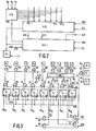
- the RBUS bus receiver includes a BUSL bus logic, a REG register and an AIC address sequence controller.
- the register REG receives from the bus
- the logic information signal SDA in the form of cycles each having an address sequence and a data sequence and a clock signal SCL.
- the address sequence identification circuit AIC receives signals leaving the register REG as well as the signals A 0 , A 1 , A 2 corresponding to the address displayed. It performs a Logic comparison between all these signals on the one hand to identify if the address displayed A 0 , A 1 , A 2 corresponds to the address sent by the bus and on the other hand to recognize an always identical flag sent in The address sequence of a cycle, this having the aim of detecting possible errors in signal transmission.
- the address sequence identification circuit AIC produces at its output a DVA identification logic signal, which is received by the BUSL bus logic.
- the BUSL BUS logic also receives the SDA Logic information signal and the SCL clock signal, in particular to recognize the start and end of each cycle. It also receives an ACN sequence end acceptance signal which is produced by the REG register when all of the bits of a sequence have been received by the REG register.
- the supply voltage V is advantageously applied to a pulse generator PG, LequeL produces a PON pulse for initialization of the bus logic BUSL, of the register REG, as well as of Memory M.
- the memory M comprises eight flip-flops M 0 to M 7 of type D, the blocking circuit BC eight doors AND and reversing AND 80 to 87, the switch block SBL four doors AND reversing 72, 78, 88 and 89 and two AND gates 28 and 58,
- the FDEC function decoder consists of an AND gate 79, and the CDEC switching decoder is decomposed into a CDEC decoder 1 processing the information of the memories M 1 and M 2 , and into a command direct from the other memories M 3 to M 7 .
- the COM switching block consists of nine controlled switches I 1 to I 9 .
- each of the flip-flops M 0 to M 7 receives at its input D an output respectively QR 0 to QR 7 of the register REG, the latter being constituted for example as will be seen in FIG. 4 by a shift register comprising flip-flops R 0 to R 7 receiving SDA Logic information in series.
- Each of the flip-flops M 0 to M 7 receives at its timing input CK the inverse LDA of the signal for loading data into memory.
- LDA proceeds to state 1 au t Orisant Loading
- LDA goes to zero, producing a falling edge active making the CK inputs of flip-flops M0 to M7.
- the flip-flops M 0 to M 7 receive on their reset input R the PON pulse produced during power-up.
- Doors 28 and 58 are blocked, and Doors 72 and 78 Allow Logic signals SCL and SDA to pass, this time corresponding to Logic levels applied to inputs L 1 and L 2 .
- a 1 Logic is present at the output of doors 81 and 82 and validates the passage of SCL and SDA through doors 88 and 89, so as to directly attack the CDEC1 decoder.
- Doors 101 to 109 validate The command of the switches I 1 to I 9 .
- M1 to M7 control the switches I 1 to I 9
- the logic levels SCL and SDA applied directly to the two inputs of the CDEC1 decoder control the switches I 1 to I 4 , according to four possible configurations for example closing one of them at a time.
- the register REG is a shift register consisting of 9 flip-flops of the DR 0 ... R 8 type , loading on a falling edge applied to their timing input CK.
- the output Q of the registers R 0 to R 7 is connected to the input D of the following flip-flop, respectively R 1 to R 8 .
- Each of the flip-flops R 0 to R 8 is clocked at its input CK via SCL of the SCL clock signal so as to operate on the rising edges of the SCL clock signal.
- the shift register, clocked by SC L receives all the bits of the address sequence A. The correct positioning of this sequence in the shift register occurs when the 1 logic enters in R 0 during initialization goes into R 8 . Then, bit A 6 is stored in R 7 and so on until A O which is stored in R 1. Bit W is always equal to zero.
- Bits A 2 , A 1 and A 0 of the sequence go be compared term by term to the bits of the same name of the address displayed thanks to three exclusive NOR gates 10, 11 and 12.
- Gate 10 receives at its inputs A 0 and Q (R 1 ), Gate 11, A 1 and Q (R2) and Gate 12, A 2 and Q (R3) - If The address A 0 , A 1 , A 2 sent in the sequence Address A is identical with the address displayed, each of doors 10, 11 and 12 outputs a 1 Logic.
- bits A 6 , A 5 , A 4 , A 3 constituted an identification flag always identical according to the sequence 1001.
- the complete identification of an address sequence is produced by a multiple AND gate 15 producing at its output a DVA identification signal and receiving at its inputs the outputs Q (R 7 ) and Q (R 4 ) and the inverted outputs P (R 5 ) and P (R 6 ) and advantageously P (R 0 ) as well as the outputs of gates 10, 11 and 12.
- Gates 10, 11, 12 and 15 constitute the address sequence identification circuit AIC.
- the output Q (R 8 ) produces a logic signal of acceptance of the end of the ACN sequence.
- the signal W which follows A 0 in the address sequence is conventionally a zero.
- first control flip-flop DC1 receiving at its input D the signal ACN available at the output Q of R 8 , and at its timing input C K The clock signal SCL, and a second control flip-flop PNT called pointer whose The inverting output P is looped over the input D, its timing input CK being connected to the output Q of the first flip-flop DC1.
- the function of the PNT pointer is to indicate whether one is in an address or data sequence of a cycle.
- a third STR and a fourth STP control toggle have the function of managing the start and the end of a cycle.
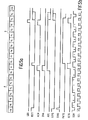
- the bus indicates the start of a cycle (see Figure 5b) by a transition from level 1 to level 0 of the SDA signal when the clock signal SCL is at level 1, and the end of a cycle by a transition of level 0 at level 1 of the SDA signal When the clock signal SCL is at level 1.
- the information-carrying transitions of the SDA signal take place When the clock signal SDA is at Logic level 0.
- the fourth bottom cule STP has the function of indicating whether the circuit is in an active state with respect to the bus or inactive. In the latter case, its output initializes the register R.
- the third flip-flop STR receives at its input D the clock signal SCL and is timed at its timing input CK by the signal SDA so as to detect the start of a cycle, while the fourth flip-flop STP receives at its input D The clock signal SCL and at its timing input CK The signal SDA inverted from SDA by an inverter 28, so as to detect the end of a cycle.
- the output Q of the third flip-flop STR is applied to the input R of reset to zero of the pointer PNT and of the fourth flip-flop STP.
- the third flip-flop STR is reset to zero by the inverse SCL of the clock signal SCL obtained by the inverter 60 whose output is connected to the input R of STR.
- the authorization signal DVA produced at the output of gate 15 is memorized by a flip-flop RS with two inverting AND gates 66 and 67 looped one over the other, that is to say that the output of gates 66 and 67 is connected respectively to an input of doors 67 and 66.
- the inverting AND gate 65 therefore receives at its inputs the signals DVA and SCL and the inverting output P of the pointer PNT, and its output is connected to the other input of the inverting AND gate 66.
- the inverting AND gate 67 receives a signal STN available at the output of an AND gate 70, the inputs of which are connected respectively to the inverting outputs P of the control switches STR and STP.
- STN 1, the DVA signal which is fugitive, remains memorized in the form of the ADC signal at the output of gate 66.
- the return of STN to state 0 is equivalent to the erasure of this memorization.
- the latter receives at its three inputs the clock signal SCL, the output Q of the first control flip-flop DC1, and the inverted output P of the pointer PNT.
- R 0 to R 8 flip-flops are initialized When STP flop stores an inactive state of the circuit (STPP), or between a sequence of addresses and a s e quence data (RST2) and in the beginning of cycle (gate AND 70).
- STPP inactive state of the circuit
- RST2 s e quence data
- a flip-flop R 9 generates at its output P an inverse authorization logic signal ACK, that is to say that the acceptance corresponds to a logic 0.
- the flip-flop R 9 is clocked at its loading authorization input CK by the clock signal SCL and receives at its input D The output of an AND gate 16 of which an input receives The acceptance signal at the end of the sequence ACN , and the other The stored identification signal ADC.
- the loading of the memory flip-flops M 0 to M 7 is obtained by an inverted loading signal LDA applied to their loading authorization inputs CK. Said loading is obtained by passing from LDA from State 1 to State 0.
- the LDA signal is obtained at the output of an inverting AND gate 33 whose inputs receive the end of sequence acceptance signal ACN, the stored identification signal ADC, and The outputs Q of the first flip-flop DC1 and of the pointer PNT. Loading is therefore authorized When an end of data sequence has been detected, whereas previously, an address sequence corresponding to that displayed by the circuit has been identified.
- the fourth flip-flop STP is set to State 1 by the output of a reversing AND gate 71 with four inputs. Its first input receives the inverted output P of STP (self-maintenance of state 1 of STP) and its second in The inverse PON of the PON pulse produced during power up. (state 1 of STP at power up).
- Its third input receives the output of an inverting AND gate 69 whose inputs are SCL, the Q output of DC1, and the Q output of the PNT pointer (setting to state 1 of STP at the end of the cycle, even in the event of bus failure).
- Its fourth input receives the output of an inverting AND gate 68 whose inputs are the Q output of DC1 and the reverse ADC of ADC, available at the output of the inverting AND gate 67 (state 1 of STP if at the end of an address sequence, no identification signal has been produced and stored).
- the bus sends The sequence A of addresses, until R 8 receives by offset
- ADC goes to state 1.
- the ACN signal also sets to state 1 the flip-flop DC1 (DC1Q) on the falling edge of the eighth clock tick.
- DC1Q goes back to 0 on the falling edge of the ninth clock stroke, because ACN is gone back to 0 on the rising edge of this same clock stroke.
- PNT Q State 1
- the bit D 7 is then stored in R 7 and so on until D 0 which is stored in R 0 .
- DC1Q 1 on the falling edge of the eighth clock tick of the sequence D, DC1Q returning to 0 on the falling edge of the next clock tick.
- the open or closed position of the switches I 1 to 1 9 is then modified in accordance with the new content of the memories M 0 to M 7 , if the OFF command is inactive or inhibited by D 0 .
- the invention is not limited to the embodiments described or shown.
- the inverted output P of the control flip-flop STR can be directly connected directly to the corresponding input of the inverting AND gate 63, the use of the AND gate 70 having the advantage of initializing the register REG in the event of untimely presence of a coincidence corresponding to the start of a cycle, while such a cycle is in progress.
- all the flip-flops of type D of the description have been chosen of the type loading on a falling edge applied to their timing input CK. It goes without saying that flip-flops loading on a rising edge could also be implemented.
- the invention is not limited to the embodiments described or shown.
- the inverted output P of the control flip-flop STR can be directly connected directly to the corresponding input of the inverting AND gate 63, the use of the AND gate 70 having the advantage of initializing the register REG in the event of untimely presence of a coincidence corresponding to the start of a cycle, while a teL cycle is in progress.
- all the flip-flops of type D of the description have been chosen of the type loading on a falling edge applied to their timing input CK. It goes without saying that flip-flops loading on a rising edge could also be implemented.
Landscapes
- Engineering & Computer Science (AREA)
- Theoretical Computer Science (AREA)
- Physics & Mathematics (AREA)
- General Engineering & Computer Science (AREA)
- General Physics & Mathematics (AREA)
- Bus Control (AREA)
- Communication Control (AREA)
- Signal Processing For Digital Recording And Reproducing (AREA)
- Dc Digital Transmission (AREA)
- Information Transfer Systems (AREA)
Applications Claiming Priority (2)
| Application Number | Priority Date | Filing Date | Title |
|---|---|---|---|
| FR8409063A FR2565751B1 (fr) | 1984-06-08 | 1984-06-08 | Circuit d'interface du type esclave |
| FR8409063 | 1984-06-08 |
Publications (2)
| Publication Number | Publication Date |
|---|---|
| EP0168076A1 true EP0168076A1 (de) | 1986-01-15 |
| EP0168076B1 EP0168076B1 (de) | 1989-09-13 |
Family
ID=9304864
Family Applications (1)
| Application Number | Title | Priority Date | Filing Date |
|---|---|---|---|
| EP85200878A Expired EP0168076B1 (de) | 1984-06-08 | 1985-06-05 | Interface-Schaltung des Sklaven-Typs |
Country Status (7)
| Country | Link |
|---|---|
| US (1) | US4815026A (de) |
| EP (1) | EP0168076B1 (de) |
| JP (1) | JPS616751A (de) |
| KR (1) | KR920003112B1 (de) |
| CA (1) | CA1234637A (de) |
| DE (1) | DE3573033D1 (de) |
| FR (1) | FR2565751B1 (de) |
Families Citing this family (6)
| Publication number | Priority date | Publication date | Assignee | Title |
|---|---|---|---|---|
| US6121949A (en) * | 1994-03-17 | 2000-09-19 | Cirrus Logic, Inc. | Method and apparatus for automatically maintaining a predetermined image quality in a display system |
| KR0184136B1 (ko) * | 1996-06-03 | 1999-05-15 | 구자홍 | 범용 마이컴을 이용한 아이 스퀘어 씨 통신 장치 |
| US5857085A (en) * | 1996-11-13 | 1999-01-05 | Cypress Semiconductor Corporation | Interface device for XT/AT system devices on high speed local bus |
| EP2056209B1 (de) * | 2000-12-11 | 2013-02-13 | Linear Technology Corporation | Schaltkreise und Verfahren zum Verbinden von Bussystemen miteinander |
| US6799233B1 (en) * | 2001-06-29 | 2004-09-28 | Koninklijke Philips Electronics N.V. | Generalized I2C slave transmitter/receiver state machine |
| US9331866B2 (en) * | 2012-04-20 | 2016-05-03 | Nxp B.V. | Network communications apparatus, system, and method |
Family Cites Families (2)
| Publication number | Priority date | Publication date | Assignee | Title |
|---|---|---|---|---|
| NL7313756A (de) * | 1972-10-11 | 1974-04-16 | ||
| NL8005976A (nl) * | 1980-10-31 | 1982-05-17 | Philips Nv | Tweedraads-bussysteem met een kloklijndraad en een datalijndraad voor het onderling verbinden van een aantal stations. |
-
1984
- 1984-06-08 FR FR8409063A patent/FR2565751B1/fr not_active Expired
-
1985
- 1985-06-05 DE DE8585200878T patent/DE3573033D1/de not_active Expired
- 1985-06-05 EP EP85200878A patent/EP0168076B1/de not_active Expired
- 1985-06-06 JP JP60121600A patent/JPS616751A/ja active Granted
- 1985-06-06 CA CA000483305A patent/CA1234637A/en not_active Expired
- 1985-06-07 KR KR1019850003969A patent/KR920003112B1/ko not_active Expired
-
1987
- 1987-10-20 US US07/112,016 patent/US4815026A/en not_active Expired - Lifetime
Non-Patent Citations (3)
| Title |
|---|
| ELECTRONIC COMPONENTS AND APPLICATIONS, vol. 3, no. 1, novembre 1980, pages 38-46, Eindhoven, NL; A.P.M. MOELANDS: "Serial I/O with the MAB8400 series microcomputers" * |
| ELONCO BULLETIN, no. 114, juin 1983, pages 2-6, Eindhoven, NL; "Samenwerking Philips en Intel. Twee nieuwe "bussen", CMOS-technologie en "CLIPS"" * |
| MINI-MICRO CONFERENCE RECORD, mai 1984, pages 23/5.1 - 23/5.10, New York, US; R.L. MITCHELL: "Super serial systems" * |
Also Published As
| Publication number | Publication date |
|---|---|
| CA1234637A (en) | 1988-03-29 |
| US4815026A (en) | 1989-03-21 |
| KR920003112B1 (ko) | 1992-04-18 |
| FR2565751A1 (fr) | 1985-12-13 |
| JPS616751A (ja) | 1986-01-13 |
| DE3573033D1 (en) | 1989-10-19 |
| KR860000596A (ko) | 1986-01-29 |
| JPH0560133B2 (de) | 1993-09-01 |
| EP0168076B1 (de) | 1989-09-13 |
| FR2565751B1 (fr) | 1986-09-05 |
Similar Documents
| Publication | Publication Date | Title |
|---|---|---|
| EP0168077B1 (de) | Interface-Schaltung des Sklaven-Typs funktionierend mit einem seriellen Bus | |
| EP0044039B1 (de) | Individualisierter, tragbarer Gegenstand der Kreditkartenart | |
| EP0554164B1 (de) | Chipkarte mit mehreren Kommunikationsprotokollen | |
| FR2707024A1 (de) | ||
| FR2479534A1 (fr) | Circuit de detection d'erreur pour une memoire | |
| FR2693860A1 (fr) | Convertisseur parallèle-série. | |
| EP0168076B1 (de) | Interface-Schaltung des Sklaven-Typs | |
| EP0267114A1 (de) | Integrierte Schaltung zur Speicherung und zur vertraulichen Verarbeitung von Informationen, die eine Antibetrugsvorrichtung enthält | |
| EP0875830A1 (de) | Prüfbare Schaltung mit geringer Zahl von Anschlüssen | |
| FR2632092A1 (fr) | Circuit de conditionnement d'ecriture d'antememoire retarde pour un systeme de microcalculateur a bus double comprenant une unite 80386 et une unite 82385 | |
| FR2528196A1 (fr) | Appareil de protection de programmes d'ordinateur | |
| CH634449A5 (fr) | Dispositif comportant un circuit emetteur et un circuit recepteur entre lesquels sont transmis des signaux electriques. | |
| CA2214098C (fr) | Coupleur pour gerer une communication entre un support de donnees portable et un dispositif d'echange de donnees, et dispositif d'echange de donnees associe | |
| EP0199294A1 (de) | Verfahren und Anordnung zur Signalisierung über eine bidirektionale digitale Übertragungsstrecke | |
| FR2680262A1 (fr) | Circuits integres pour carte a puce et carte a plusieurs puces utilisant ces circuits. | |
| EP0359607B1 (de) | Zentrale Datenverarbeitungseinheit für ein Datenverarbeitungssystem | |
| EP0344052B1 (de) | Modularer Speicher | |
| EP0017586A1 (de) | Datenverarbeitungseinrichtung mit zwei Speichern mit direktem Zugriff, die sowohl in Lese- wie in Schreibmodus zusammenarbeiten | |
| WO2003034246A2 (fr) | Dispositif de transmission de donnees asynchrones comprenant des moyens de controle de deviation d'horloge | |
| EP0246168A1 (de) | Einschaltungsvorrichtung zum unabhängigen Verbinden von Zusatzspeichern mit einem Datenverarbeitungssystem | |
| EP1330781A1 (de) | Schaltung zur detektion und umsetzung einer datenspur | |
| FR2803059A1 (fr) | Lecteur de cartes a puces synchrones | |
| FR2582423A1 (fr) | Memoire tampon a interposer entre deux systemes synchrones a vitesses differentes | |
| FR2558615A1 (fr) | Controleur integre d'unite a disque souple | |
| FR2711817A1 (fr) | Interface de connexion entre un microprocesseur et un bus. |
Legal Events
| Date | Code | Title | Description |
|---|---|---|---|
| PUAI | Public reference made under article 153(3) epc to a published international application that has entered the european phase |
Free format text: ORIGINAL CODE: 0009012 |
|
| AK | Designated contracting states |
Designated state(s): DE FR GB IT |
|
| 17P | Request for examination filed |
Effective date: 19860530 |
|
| RAP1 | Party data changed (applicant data changed or rights of an application transferred) |
Owner name: N.V. PHILIPS' GLOEILAMPENFABRIEKEN Owner name: RTC-COMPELEC |
|
| 17Q | First examination report despatched |
Effective date: 19880812 |
|
| GRAA | (expected) grant |
Free format text: ORIGINAL CODE: 0009210 |
|
| AK | Designated contracting states |
Kind code of ref document: B1 Designated state(s): DE FR GB IT |
|
| REF | Corresponds to: |
Ref document number: 3573033 Country of ref document: DE Date of ref document: 19891019 |
|
| ITF | It: translation for a ep patent filed | ||
| GBT | Gb: translation of ep patent filed (gb section 77(6)(a)/1977) | ||
| REG | Reference to a national code |
Ref country code: FR Ref legal event code: CA |
|
| PLBE | No opposition filed within time limit |
Free format text: ORIGINAL CODE: 0009261 |
|
| STAA | Information on the status of an ep patent application or granted ep patent |
Free format text: STATUS: NO OPPOSITION FILED WITHIN TIME LIMIT |
|
| 26N | No opposition filed | ||
| REG | Reference to a national code |
Ref country code: FR Ref legal event code: CD |
|
| ITTA | It: last paid annual fee | ||
| ITPR | It: changes in ownership of a european patent |
Owner name: CAMBIO RAGIONE SOCIALE;PHILIPS ELECTRONICS N.V. |
|
| REG | Reference to a national code |
Ref country code: FR Ref legal event code: CD |
|
| REG | Reference to a national code |
Ref country code: FR Ref legal event code: TP |
|
| REG | Reference to a national code |
Ref country code: GB Ref legal event code: IF02 |
|
| PGFP | Annual fee paid to national office [announced via postgrant information from national office to epo] |
Ref country code: DE Payment date: 20020821 Year of fee payment: 18 |
|
| PGFP | Annual fee paid to national office [announced via postgrant information from national office to epo] |
Ref country code: FR Payment date: 20030625 Year of fee payment: 19 |
|
| PGFP | Annual fee paid to national office [announced via postgrant information from national office to epo] |
Ref country code: GB Payment date: 20030627 Year of fee payment: 19 |
|
| PG25 | Lapsed in a contracting state [announced via postgrant information from national office to epo] |
Ref country code: DE Free format text: LAPSE BECAUSE OF NON-PAYMENT OF DUE FEES Effective date: 20040101 |
|
| PG25 | Lapsed in a contracting state [announced via postgrant information from national office to epo] |
Ref country code: GB Free format text: LAPSE BECAUSE OF NON-PAYMENT OF DUE FEES Effective date: 20040605 |
|
| GBPC | Gb: european patent ceased through non-payment of renewal fee |
Effective date: 20040605 |
|
| PG25 | Lapsed in a contracting state [announced via postgrant information from national office to epo] |
Ref country code: FR Free format text: LAPSE BECAUSE OF NON-PAYMENT OF DUE FEES Effective date: 20050228 |
|
| REG | Reference to a national code |
Ref country code: FR Ref legal event code: ST |