EP0168643A2 - Dispositif pour l'inspection de pastilles de semi-conducteurs - Google Patents
Dispositif pour l'inspection de pastilles de semi-conducteurs Download PDFInfo
- Publication number
- EP0168643A2 EP0168643A2 EP85107360A EP85107360A EP0168643A2 EP 0168643 A2 EP0168643 A2 EP 0168643A2 EP 85107360 A EP85107360 A EP 85107360A EP 85107360 A EP85107360 A EP 85107360A EP 0168643 A2 EP0168643 A2 EP 0168643A2
- Authority
- EP
- European Patent Office
- Prior art keywords
- scanning
- light
- examination
- wafer
- plane
- Prior art date
- Legal status (The legal status is an assumption and is not a legal conclusion. Google has not performed a legal analysis and makes no representation as to the accuracy of the status listed.)
- Granted
Links
Images
Classifications
-
- G—PHYSICS
- G03—PHOTOGRAPHY; CINEMATOGRAPHY; ANALOGOUS TECHNIQUES USING WAVES OTHER THAN OPTICAL WAVES; ELECTROGRAPHY; HOLOGRAPHY
- G03F—PHOTOMECHANICAL PRODUCTION OF TEXTURED OR PATTERNED SURFACES, e.g. FOR PRINTING, FOR PROCESSING OF SEMICONDUCTOR DEVICES; MATERIALS THEREFOR; ORIGINALS THEREFOR; APPARATUS SPECIALLY ADAPTED THEREFOR
- G03F7/00—Photomechanical, e.g. photolithographic, production of textured or patterned surfaces, e.g. printing surfaces; Materials therefor, e.g. comprising photoresists; Apparatus specially adapted therefor
- G03F7/70—Microphotolithographic exposure; Apparatus therefor
- G03F7/70483—Information management; Active and passive control; Testing; Wafer monitoring, e.g. pattern monitoring
- G03F7/70605—Workpiece metrology
- G03F7/70616—Monitoring the printed patterns
- G03F7/70641—Focus
-
- G—PHYSICS
- G01—MEASURING; TESTING
- G01N—INVESTIGATING OR ANALYSING MATERIALS BY DETERMINING THEIR CHEMICAL OR PHYSICAL PROPERTIES
- G01N21/00—Investigating or analysing materials by the use of optical means, i.e. using sub-millimetre waves, infrared, visible or ultraviolet light
- G01N21/84—Systems specially adapted for particular applications
- G01N21/88—Investigating the presence of flaws or contamination
- G01N21/95—Investigating the presence of flaws or contamination characterised by the material or shape of the object to be examined
- G01N21/9501—Semiconductor wafers
-
- G—PHYSICS
- G02—OPTICS
- G02B—OPTICAL ELEMENTS, SYSTEMS OR APPARATUS
- G02B21/00—Microscopes
- G02B21/0004—Microscopes specially adapted for specific applications
- G02B21/002—Scanning microscopes
Definitions
- the invention relates to a device for wafer inspection with the generic features mentioned in the preamble of claim 1.
- a device of this type is known from the scientific publication by Karl L. Harris et al., Solid State Technology, February 1984, page 159 ff.
- a wafer that is to say a semiconductor plate provided for the production of highly integrated circuits, which can typically have dimensions of approximately 15 ⁇ 15 cm (6 “ ⁇ 6“), can be shown enlarged by means of a television picture display;
- the image evaluation of the television picture is done electronically with a computer with high processing speed.
- the Vidikon tube used to record the television picture can only distinguish about 30 different gray levels, which results in limitations with regard to image contrast, image sharpness and ultimately also the resolution.
- a focusing of the scanning electron beam is only possible on a certain examination level of the wafer, with the result that the television picture inevitably has considerable blurring for this reason as well.
- a change in the level of the sharp representation is possible at most by lifting or deflecting the wafer; however, the mechanical devices required for this work slowly and additionally limit the processing speed.
- no further information can be obtained with the known device.
- the optical scanning of the wafer surface prevents charging of individual areas of the wafer, which could lead to a change in the electrical properties of the finished component.
- the device according to the invention allows a much faster scanning of the examination area, with the help of an electronically controllable active mirror the examination planes can be changed practically without inertia and a multitude of layer-by-layer scans of the examination object are possible, which can be processed to a precise, high-contrast and high-resolution image resolution.
- the use of a laser scanning microscope to focus the laser scanning light bundle allows a narrow limitation of the depth (depth of field) of the examination area and thus a high-resolution subdivision of the same into individually representable layers, with the evaluation of the image data that can be obtained an accurate topographical representation of the wafer surface allowed.
- the detection light is limited to the depth of field, a high signal-to-noise ratio is achieved, which allows the examination area to be scanned at a high sampling frequency.
- the use of an active mirror for shifting the focus of the scanning light provides the advantage that devices for raising and lowering the wafer for setting certain scanning planes can be dispensed with.
- the features of claim 2 indicate a favorable arrangement of the same within the scanning beam path.
- the intensity of the scanning luminous flux can be increased in a targeted manner.
- the preferred embodiment of the device according to the invention outlined by the features of claim 7 in terms of its basic structure and specified in more detail by the features of claims 8-11 conveys the advantage that An evaluation of the point image functions of successively scanned image elements detected by a second scanning device makes it possible to auto-focus the scanning beam of the scanning device provided for image scanning, as a result of which sharp profile representations of the wafer surface can be generated and also precise information regarding the layer thickness of oxide layers can be obtained to let.
- a transport device designed according to claim 16 is provided for the wafer, it is possible to dispense with a galvanometer mirror required for Y-beam deflection as part of the scanning device.
- a line-shaped scanning area can also be compared with a predetermined target structure with the aid of a so-called convolver, which conveys a non-linear superposition of surface waves propagating in the opposite direction in a piezoelectric material, one of which is the target structure and the other
- the amplitude profile corresponding to the intensity profile of the scanning light measured for the real structure is impressed, so that a measurement of the correspondence of the structures mentioned can be obtained from a measurement of the integral of the correlation function of these surface waves.
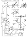
- the device 10 according to the invention shown in FIG. 1, to the details of which reference is expressly made, is intended for a so-called wafer inspection, i.e. for production control in the manufacture of highly integrated semiconductor components that are manufactured in a multitude of process steps. Structures are created on a so-called wafer 11 - a silicon plate with a diameter of up to 6 inches in vapor deposition, etching and oxidation as well as diffusion and doping processes, which correspond to an extremely complex arrangement of electronic circuit elements. With the aid of the device 10, the structures characteristic of certain stages of the manufacturing process should be comparable as quickly as possible to target structures in order to reliably identify manufacturing defects and to be able to remove a wafer with such errors in good time from the production process.
- the device 10 is a so-called laser scanning microscope (laser scanning microscope), which uses line-by-line and point-by-line scanning within each line of the examination object or region and a representation of the examination region which is carried out in principle by analogy with the representation of a television image 16 works, which is indicated schematically in FIG. 1 by the focusing plane of a microscope objective 17, which is specifically the surface of a wafer structure produced after a certain process step.
- laser scanning microscope laser scanning microscope
- the individual - essentially point-shaped - elementary areas of the examination area 16 are sequentially illuminated with laser light in the above-mentioned line or point grid, and the intensity of the reflection or scattered light emanating from this is measured for each elementary area, using a photoelectric detector , specifically a photomultiplier 19 is detected separately for each picture element.
- the intensity values detected in this way of the laser light reflected by the examination object are input into an image memory 21 in synchronism with the light scanning of the examination object and are kept there for further processing - image display and possibly arithmetic processing of the intensity data.
- This laser 13 is a so-called cw laser that emits continuously.
- the primary beam of this helium-cadmium laser 22 is represented in FIG. 1 by its central beam 23 and its edge beams 24 and 26, which are shown in dash-dotted lines.
- the primary beam 23, 24, 26 of the He-Cd laser 22 is essentially a parallel beam with a beam cross section of approximately 1 mm 2 .
- a bundle shape is suitable for the further utilization of the laser light in the sense of an adaptation of the bundle cross-section to the optical devices available for further optical processing and in the sense of influencing the convergence of the to be explained in more detail below Laser light beam adjustable.
- the marginal rays of the output light bundle of the beam shaping optics 27, which has a larger cross section at its output 28 than at its input 29, are denoted by 24 'and 26'.
- the output light bundle 23, 24 ', 26' of the beam shaping optics 27 is fed to a scanning (scan) device, designated overall by 31, which on the one hand conveys a "horizontal” and on the other hand a “vertical” beam deflection, which in the aforementioned scanning Raster allows the scanning of the examination area 16 in the X and Y coordinate directions.
- a scanning (scan) device designated overall by 31, which on the one hand conveys a "horizontal” and on the other hand a “vertical” beam deflection, which in the aforementioned scanning Raster allows the scanning of the examination area 16 in the X and Y coordinate directions.
- a so-called polygon mirror 32 is provided as the horizontal deflection element, the facets 33 of which delimit a regular octagon in the illustration in FIG. 1.
- the polygon mirror 32 has 24 facets 33 in a regular polygonal arrangement to one another.
- the polygon mirror 32 can be driven to rotate by means of an electric motor 34, the rotation frequency of this polygon mirror 32 being synchronized in a manner which will be explained in more detail below with the storage of the output signals of the photomultiplier 19 in the image memory 21, in which the image of the examination area 16 is in digital format is saved.
- the Y deflection of the laser light bundle 23, 24 ', 26' is, in the direction of propagation of the laser light bundle 23, 24 ', 26' shown by the arrow 36, downstream of the X deflection 32, 34, and is achieved by means of a galvanometer mirror 38 pivotably driven about a horizontal axis 37 in a manner known per se.
- the facet surfaces 33 of the polygon mirror 32 are imaged on the reflecting surface 42 of the galvanometer mirror 38 in a so-called telecentric beam path, which is realized by means of two lenses 39 and 41.
- a deflecting mirror 43 arranged between the exit lens 41 of this telecentric beam path and the galvanometer mirror 38 is only provided to achieve a favorable beam path geometry.
- the reflecting surface 42 of the galvanometer mirror 38 is imaged on the entrance pupil 47 of the microscope objective 17, which in turn the laser light passing through the entrance pupil 47 as a parallel bundle or almost parallel bundle of light Examination level 16 focused.
- the laser light reflected or scattered at the structures of the examination object present in the focusing or examination plane 16 is reflected back into the beam path explained so far and by means of a partially transparent mirror 48, usually a semitransparent mirror, between the polygon mirror 32 and the exit 28 of the beam shaping optics 27 is arranged, coupled out in the direction of arrow 49 from the scanning beam path.
- a partially transparent mirror 48 usually a semitransparent mirror
- This decoupled light bundle 23 ', 24', 26 ' is focused by means of a further microscope objective 51;
- a pinhole 53 is arranged in the focal plane 52 of this further microscope objective 51, which mediates a bundle limitation in such a way that through this pinhole 53 only such laser light can pass through as useful light used for the intensity measurement, which comes from the area of the focal plane of the microscope lens 17 forming the examination plane 16 that corresponds to the depth of field area of the microscope lens 17.
- the photomultiplier 19 Seen in the direction of propagation 49 of the laser light coupled out of the illuminating beam path, the photomultiplier 19 is arranged behind the pinhole 53 and generates an output signal proportional to the intensity of the laser light reflected back into the scanning beam path by the object under examination.
- the output signals of the photomultiplier 19, each assigned to an elementary area of the examination plane 16, are controlled in the image memory 21 by a synchronizing device 54 which conveys the appropriate control of the rotation of the polygon mirror 32 and of the pivoting movements of the galvanometer mirror 38, the latter by means of a pivot drive 56.
- the examination field is broken down into 512 x 2,048 pixels, analogously to the generation of a conventional television image. Accordingly 512 image lines are scanned and 2 048 image points within each line.
- the size i.e. the extent of the pixels in the "horizontal" and “vertical” direction results from the size of the image field, divided by the number of pixels per line or image height divided by the number of lines.
- the size of the image field varies between 100 ⁇ m and several mm; the pixel size accordingly varies between 0.05 ⁇ m and a few ⁇ m.
- the scanning of the examination area 16 takes place so quickly that the image field is scanned in 40 ms, a field being scanned in each 20 ms, one of which contains the odd and the other the even line numbers. These two fields are then superimposed on one another in a manner known per se.
- An electro-optical or acousto-optical modulator is also synchronized with the read-in clock, by means of which the intensity of the laser light thrown into the examination plane 16 can be modulated. This makes it possible to illuminate areas of the examination field with a higher intensity than the remaining part of the examination field. This is particularly important if individual areas are to be imaged with high contrast,
- a so-called active mirror 57 is provided, to which a - positive or negative - refractive power can be impressed by electrical control, which changes the position of the lens Examination plane 16, seen perpendicular to this, within a range of + 10 ⁇ m, based on a preselected position of the examination plane 16, is made possible.
- this active mirror 57 acts as a flat mirror in the non-activated state.
- the active mirror 57 is arranged in a pupil plane 47 ′ corresponding to the plane of the entrance pupil 47 of the microscope objective 17. It is illuminated via a partially transparent - semi-transparent - mirror 58 of the beam shaping optics 27, at which the output light beam 23, 24, 26 of the laser 22 expanded by means of a telecentric lens arrangement 59, 61, which comprises the two converging lenses 59 and 61 of different focal lengths active mirror 57 is deflected out.
- the light flux reflected by the active mirror 57 represented by the marginal rays 26 ′′ and 24 ′′ and passing through the partially transparent mirror 58, is switched to the one for the further, already explained, utilization by means of a further telecentric arrangement of lenses 62 and 63 of the beam shaping optics 27 brought suitable cross-section of the laser light flux, with which the laser light bundle 23, 24 ', 26', exits at the output 28 of the beam shaping optics 27.
- the device 10 explained so far can thus, by appropriately controlling the active mirror 57, possibly program-controlled, quickly and precisely to scan different, e.g. Equidistantly staggered examination levels 16, 16 'and 16' 'can be set, the images of which, provided that the image memory 21 has sufficient capacity, can be stored in their entirety.
- the content of the image memory 21 can then be used to represent any sectional planes through the total of the examined examination area, which can run obliquely to the scanned examination planes or also perpendicular to them.
- a characteristic feature of the device 10 according to FIG. 1 is, as already mentioned, the confocal arrangement of the pinhole 53 to the focal plane 16 of the microscope objective 17 marking the examination plane, which means that only light can pass through the pinhole that comes from a depth of field can pass through the microscope objective 53 designable image.
- the light streams reflected or scattered from other areas, which - as seen in the direction of propagation of the laser light - lie in front of or behind the focal plane 16 of the microscope objective, are thrown onto the edge of the pinhole 53 by the confocal beam path and thus shadowed against the photomultiplier 19.
- the thickness of the examination area 16 corresponding to the depth of field area of the microscope objective 17 is small. In typical cases it is between 0.05 ⁇ m and 1pm.
- the microscope objective 17 has a focal length of 5 mm and a numerical aperture of 0.9.
- the diameter of the laser light bundle 23, 24 ', 26', which is focused into the examination plane 16 by the microscope objective 17, is up to 6 mm.
- a further scanning device designated 64 in total, which, in principle, in the same way as explained above with reference to the scanning device 31, enables partial or complete scanning of the examination image field.
- This scanning device 64 comprises, as scanning elements, a first galvanometer mirror 66 which extends around a horizontal, i.e. axis 67 parallel to the plane of propagation of the scanning light is pivotable and mediates the Y deflection of the scanning light, and a second galvanometer mirror 68 which is pivotable about an axis 69 running perpendicular to the plane of propagation of the scanning light and accordingly the X deflection, ie the line deflection conveys.
- This partial luminous flux 23 ′′, 24 ′′, 26 ′′ is in the geometry shown in FIG. 1 via a first. partially transmissive deflection mirror 71 and a second partially transmissive deflection mirror 72 as well as via the further scanning device 64 and a further partially transmissive mirror 73 are coupled into the beam path provided for imaging the examination area 16, this coupling of the further scanning luminous flux between the galvanometer mirror 38 of the first scanning Device 31 and one lens 44 of the telecentric lens arrangement 44, 46, which is arranged in front of the entrance pupil 47 of the microscope objective 17.
- the intensity of the partial luminous flux 23 ′′, 24 ′′, 26 ′′ used for the additional scanning is only about 10% of the intensity of the output luminous flux of the He-Cd laser.
- 2 modulators 56 'and 56' ' are provided in the arrangement shown in FIG. 1 with respect to a partially transparent mirror 70 for intensity control of the scanning light flows.
- the further scanning device 64 is operated asynchronously to the scanning device 31 and with a significantly lower scanning frequency.
- the light reflected from the examination object by reflection or scattering into the beam path of the further scanning device 66 is detected with a two-dimensional (2 D) matrix arrangement of photoelectric receivers, preferably a diode matrix 73, with regard to its two-dimensional spatial intensity distribution, the intensity distribution of each of radiation reflected back from an illuminated picture element is measured and stored for further processing, ie the so-called point spread function (PS function) is recorded. From the PS function recorded in this way can.
- 2 D two-dimensional
- a deviation of the course of the wave front of the scanning light passing through parts of the examination object from the ideal course to be expected according to the geometrical-optical boundary conditions can be calculated.
- the determination of the PS function is particularly interesting because the spatial intensity distribution of the point image allows conclusions to be drawn about structures whose characteristic dimensions are smaller than those of the picture element illuminated as a scanning point. In this way, edge structures can be detected precisely and the smallest dirt particles can be recognized.
- the point image function measured by means of the further scanning device 64 is also used for point-by-point auto-focusing of the scanning light bundle on the structure erected on the wafer 11.
- a computer 74 compares the measured intensity distribution with a - ideal - point image function which is characteristic of the focusing of the scanning light beam on the scanned surface. From this comparison, control signals for compensatory control of the active mirror 57 are generated in such a way that the intensity distribution measured by means of the further scanning device 64 is "adjusted" to the ideal point image function in a good approximation.
- control signals required for this can be evaluated in units of a distance from a reference plane according to the amount and sense of change. As a result, the layer thicknesses or heights of surface profiles can be recorded continuously.
- the surface structure of the wafer 11 can thus be represented in all coordinate directions (X and Y direction by scanning, the Z direction by evaluating the point image function).
- the light field profile now becomes a wave front profile consistent with this field profile at the entrance pupil 47 of the microscope objective 17, ie a phase factor ⁇ 1 (x, y) consistent therewith.
- this phase factor is now used to describe the light field at the location of the entrance pupil and, as previously described, the wave field in the focal plane of the microscope objective 17 is again calculated; Furthermore, the amplitude factors are replaced by the roots of the measured intensity values and the new phase factor ⁇ 2 (x, y) is calculated.
- control signals for controlling the active mirror 57 can be generated with the aid of the computer 74 and the adjusting device 76, in such a way that the measured one Intensity distribution coincides with the intensity distribution in the focal plane resulting from an ideal field distribution at the location of the entrance pupil 47.
- test light with a broadband spectral distribution can also be coupled into the beam path of the further scanning device 64.
- the layer thickness of these structures is recorded point by point, and up to 1,000 layer thickness values per second can be measured.
- the layer thickness measurement is carried out in this case according to the principle of the so-called white light interference, a diode-line spectrometer 78 being provided for determining the wavelengths of constructive interference, the light reflected by the examination object being coupled into its entry slit 79 via a partially transparent mirror.
- An XBO lamp (high-pressure xenon lamp) is expediently used as the white light source.
- the device 10 can also be used to record the spatial distribution of luminescent molecules present in the examination area.
- a filter is arranged between the partially transparent mirror 48, via which the light used for the detection is coupled out from the scanning beam path, and the photomultiplier 19, which filter is suitable for the exciting UV radiation of the laser 22 and expediently also for whose radiation emitted in the visible spectral range is opaque.
- the measurement of the luminescence radiation is particularly interesting for determining the distribution of photoresist residues on the wafer 11.
- a filter 82 suitable for the luminescence measurement is expediently used, as shown in FIG. indicated by dashed lines, arranged between the partially transparent mirror 48 and the lens 51, in whose focal plane 52 the pinhole 53 is located.
- the scanning of the examination field can also be carried out as shown schematically in FIG. 3 that the wafer, e.g. can be moved on an X, Y coordinate carriage in the X and Y direction and is moved along a meandering or rectangular wave-shaped path.
- the wafer e.g. can be moved on an X, Y coordinate carriage in the X and Y direction and is moved along a meandering or rectangular wave-shaped path.
- the step size of the wafer movement is selected to be equal to the amplitude of the beam deflection.
- the movement stroke of the wafer 11 corresponds in each case to the extent of the selected examination area.
- a comparison of a line-shaped scanning area with a predetermined target structure of the same, which can be carried out very quickly, can also be carried out using a so-called convolver.
- Function of such a constructioniatas is based on a nonlinear superposition of surface acoustic waves, to which an amplitude profile can be impressed which corresponds to the intensity distribution of the light reflected back onto the detector of the scanning device, which distribution is detected within a scanning line.
- Acoustic waves running in the opposite direction are generated in the convolver, one of which corresponds to the target structure with regard to its amplitude profile and the other to the measured intensity profile.
- the integral of the correlation function arising from the nonlinear superposition of these acoustic waves is maximum, as can be determined by a voltage that can be picked up from a cover electrode of the convolver made of piezoelectric material. From the value of the integral of the correlation function of the two surface waves measured in this way, the agreement of the scanned structure with the target structure can thus be determined.
- Such a turret device can be used not only for the purpose of detecting structural defects, but also for the purpose of analog auto-focusing of the scanning beam path on the surface of the investigating structure, as explained above.
Landscapes
- Physics & Mathematics (AREA)
- General Physics & Mathematics (AREA)
- Chemical & Material Sciences (AREA)
- Analytical Chemistry (AREA)
- Immunology (AREA)
- Life Sciences & Earth Sciences (AREA)
- Biochemistry (AREA)
- General Health & Medical Sciences (AREA)
- Health & Medical Sciences (AREA)
- Pathology (AREA)
- Optics & Photonics (AREA)
- Testing Or Measuring Of Semiconductors Or The Like (AREA)
- Investigating Materials By The Use Of Optical Means Adapted For Particular Applications (AREA)
- Length Measuring Devices By Optical Means (AREA)
- Testing Of Individual Semiconductor Devices (AREA)
- Microscoopes, Condenser (AREA)
Priority Applications (1)
| Application Number | Priority Date | Filing Date | Title |
|---|---|---|---|
| AT85107360T ATE56275T1 (de) | 1984-06-14 | 1985-06-14 | Geraet zur wafer-inspektion. |
Applications Claiming Priority (2)
| Application Number | Priority Date | Filing Date | Title |
|---|---|---|---|
| DE3422143A DE3422143A1 (de) | 1984-06-14 | 1984-06-14 | Geraet zur wafer-inspektion |
| DE3422143 | 1984-06-14 |
Publications (3)
| Publication Number | Publication Date |
|---|---|
| EP0168643A2 true EP0168643A2 (fr) | 1986-01-22 |
| EP0168643A3 EP0168643A3 (en) | 1987-01-07 |
| EP0168643B1 EP0168643B1 (fr) | 1990-09-05 |
Family
ID=6238367
Family Applications (1)
| Application Number | Title | Priority Date | Filing Date |
|---|---|---|---|
| EP85107360A Expired - Lifetime EP0168643B1 (fr) | 1984-06-14 | 1985-06-14 | Dispositif pour l'inspection de pastilles de semi-conducteurs |
Country Status (5)
| Country | Link |
|---|---|
| US (1) | US4732473A (fr) |
| EP (1) | EP0168643B1 (fr) |
| JP (1) | JPS6188107A (fr) |
| AT (1) | ATE56275T1 (fr) |
| DE (2) | DE3422143A1 (fr) |
Cited By (10)
| Publication number | Priority date | Publication date | Assignee | Title |
|---|---|---|---|---|
| DE3903560A1 (de) * | 1988-02-09 | 1989-08-17 | Zeiss Carl Fa | Mikroskop mit einem geraet zur vermessung mikroskopischer strukturen |
| EP0249800A3 (en) * | 1986-06-14 | 1989-12-13 | Battelle-Institut E.V. | Apparatus for illuminating components of transparent material used in the inspection for defects |
| EP0260522A3 (en) * | 1986-09-17 | 1990-04-25 | Kabushiki Kaisha Toshiba | Method and apparatus for scanning a laser beam to examine the surface of semiconductor wafer |
| EP0444450A1 (fr) * | 1990-03-02 | 1991-09-04 | International Business Machines Corporation | Commande des outils lithographiques par d'image latente |
| EP0502752A1 (fr) * | 1991-03-04 | 1992-09-09 | Dilor | Appareil de spectrométrie |
| WO1993024854A1 (fr) * | 1992-05-25 | 1993-12-09 | Braintech Planung Und Bau Von Industrieanlagen Gesellschaft Mbh | Objectif de balayage |
| EP0606479A4 (en) * | 1991-10-01 | 1994-07-27 | Ohmi Tadahiro | Analyzer. |
| EP0620468A1 (fr) * | 1993-04-15 | 1994-10-19 | Kowa Co. Ltd. | Microscope de balayage à laser |
| US5822061A (en) * | 1992-01-20 | 1998-10-13 | Dilor | Spectrometry apparatus |
| CN112099218A (zh) * | 2020-09-18 | 2020-12-18 | 吉林大学 | 一种飞秒激光系统图像调焦方法 |
Families Citing this family (54)
| Publication number | Priority date | Publication date | Assignee | Title |
|---|---|---|---|---|
| US4910690A (en) * | 1986-02-14 | 1990-03-20 | Citizen Watch Co., Ltd. | Micro-dimensional measurement apparatus |
| JPH07107481B2 (ja) * | 1987-05-21 | 1995-11-15 | アンリツ株式会社 | 変位測定装置 |
| US4901718A (en) * | 1988-02-02 | 1990-02-20 | Intelligent Surgical Lasers | 3-Dimensional laser beam guidance system |
| US5076691A (en) * | 1988-04-27 | 1991-12-31 | Hewlett-Packard Company | Non-reflecting structures for surface scanners |
| US4977330A (en) * | 1989-02-13 | 1990-12-11 | Batchelder Tom W | In-line photoresist thickness monitor |
| US5153445A (en) * | 1991-07-22 | 1992-10-06 | General Motors Corporation | Method and apparatus for measuring orange peel and texture in painted surfaces |
| US5246435A (en) * | 1992-02-25 | 1993-09-21 | Intelligent Surgical Lasers | Method for removing cataractous material |
| US5737122A (en) * | 1992-05-01 | 1998-04-07 | Electro Scientific Industries, Inc. | Illumination system for OCR of indicia on a substrate |
| US5231536A (en) * | 1992-05-01 | 1993-07-27 | Xrl, Inc. | Robust, LED illumination system for OCR of indicia on a substrate |
| US5396332A (en) * | 1993-02-08 | 1995-03-07 | Ciszek; Theodoer F. | Apparatus and method for measuring the thickness of a semiconductor wafer |
| US5448364A (en) * | 1993-03-22 | 1995-09-05 | Estek Corporation | Particle detection system with reflective line-to-spot collector |
| US5742326A (en) * | 1993-09-28 | 1998-04-21 | Nikon Corporation | Focus adjustable image reading device for calculating a focus position of a source document |
| US5656186A (en) * | 1994-04-08 | 1997-08-12 | The Regents Of The University Of Michigan | Method for controlling configuration of laser induced breakdown and ablation |
| WO1995035506A2 (fr) * | 1994-06-17 | 1995-12-28 | Kensington Laboratories, Inc. | Lecteur de marques gravees |
| US5715326A (en) * | 1994-09-08 | 1998-02-03 | Neopath, Inc. | Cytological system illumination integrity checking apparatus and method |
| DE69530072T2 (de) * | 1994-12-08 | 2004-03-04 | Molecular Dynamics, Sunnyvale | System zur fluoreszenzabbildung unter verwendung eines objektivs mit makroabtastung |
| EP0902885A4 (fr) * | 1996-05-16 | 2006-09-27 | Affymetrix Inc | Systemes et procedes de detection de produits marques |
| DE19640496A1 (de) * | 1996-10-01 | 1998-04-02 | Leica Lasertechnik | Verfahren zur Oberflächenvermessung mittels Konfokalmikroskopie |
| US6201601B1 (en) * | 1997-09-19 | 2001-03-13 | Kla-Tencor Corporation | Sample inspection system |
| US6263098B1 (en) * | 1998-09-11 | 2001-07-17 | The United States Of America As Represented By The Secretary Of The Army | Determination of functionality for integrated circuit modules |
| US6999183B2 (en) * | 1998-11-18 | 2006-02-14 | Kla-Tencor Corporation | Detection system for nanometer scale topographic measurements of reflective surfaces |
| US6867406B1 (en) * | 1999-03-23 | 2005-03-15 | Kla-Tencor Corporation | Confocal wafer inspection method and apparatus using fly lens arrangement |
| US6050687A (en) * | 1999-06-11 | 2000-04-18 | 20/10 Perfect Vision Optische Geraete Gmbh | Method and apparatus for measurement of the refractive properties of the human eye |
| US6707545B1 (en) * | 1999-09-07 | 2004-03-16 | Applied Materials, Inc. | Optical signal routing method and apparatus providing multiple inspection collection points on semiconductor manufacturing systems |
| US6693708B1 (en) * | 1999-09-07 | 2004-02-17 | Applied Materials, Inc. | Method and apparatus for substrate surface inspection using spectral profiling techniques |
| DE19957418B4 (de) * | 1999-11-29 | 2016-02-04 | Leica Microsystems Cms Gmbh | Verfahren zur lichtoptischen Abtastung eines Objekts und Rastermikroskop zur Anwendung des Verfahrens |
| US6341009B1 (en) | 2000-02-24 | 2002-01-22 | Quantronix Corporation | Laser delivery system and method for photolithographic mask repair |
| US6220707B1 (en) | 2000-02-25 | 2001-04-24 | 20/10 Perfect Vision Optische Geraete Gmbh | Method for programming an active mirror to mimic a wavefront |
| US6714892B2 (en) * | 2001-03-12 | 2004-03-30 | Agere Systems, Inc. | Three dimensional reconstruction metrology |
| KR100420241B1 (ko) * | 2001-06-20 | 2004-03-02 | (주)시아이센서 | 이미지 센서용 반도체 칩 테스트 방법 및 그 장치 |
| DE10157244B4 (de) * | 2001-11-22 | 2006-05-04 | Leica Microsystems Semiconductor Gmbh | Verfahren und Vorrichtung zur Defektanalyse von Wafern |
| US7158235B2 (en) * | 2001-12-05 | 2007-01-02 | Rudolph Technologies, Inc. | System and method for inspection using white light interferometry |
| US7139631B2 (en) * | 2003-03-12 | 2006-11-21 | Asml Holding N.V. | Method and system to compensate for scanner system timing variability in a semiconductor wafer fabrication system |
| DE10323923A1 (de) * | 2003-05-22 | 2004-12-16 | Carl Zeiss Jena Gmbh | Einstellbares Pinhole, insbesondere für ein Laser-Scanning-Mikroskop |
| US6947454B2 (en) * | 2003-06-30 | 2005-09-20 | Electro Scientific Industries, Inc. | Laser pulse picking employing controlled AOM loading |
| ES2277473B1 (es) * | 2004-01-30 | 2008-07-16 | Consejo Sup. Investig. Cientificas | Composicion coherente de señales por correccion focal progresiva. |
| US7618415B2 (en) * | 2004-04-09 | 2009-11-17 | Technolas Perfect Vision Gmbh | Beam steering system for corneal laser surgery |
| US7420669B2 (en) * | 2004-07-01 | 2008-09-02 | Midwest Research Institute | Optic probe for semiconductor characterization |
| US20060114948A1 (en) * | 2004-11-29 | 2006-06-01 | Lo Ho W | Workpiece processing system using a common imaged optical assembly to shape the spatial distributions of light energy of multiple laser beams |
| TW200630604A (en) * | 2005-01-06 | 2006-09-01 | Matsushita Electric Industrial Co Ltd | Method and apparatus for inspection of optical component |
| US7292393B2 (en) | 2005-01-12 | 2007-11-06 | Kla-Tencor Technologies Corporation | Variable illuminator and speckle buster apparatus |
| DE102005061834B4 (de) | 2005-12-23 | 2007-11-08 | Ioss Intelligente Optische Sensoren & Systeme Gmbh | Vorrichtung und Verfahren zum optischen Prüfen einer Oberfläche |
| GB0611156D0 (en) * | 2006-06-07 | 2006-07-19 | Qinetiq Ltd | Optical inspection |
| US7834259B2 (en) * | 2008-04-10 | 2010-11-16 | Ego Industries, Inc. | Adjustable folding leg for bass drum |
| RU2372690C1 (ru) * | 2008-04-28 | 2009-11-10 | Государственное образовательное учреждение высшего профессионального образования "Санкт-Петербургский государственный электротехнический университет "ЛЭТИ" им. В.И. Ульянова (Ленина)" (СПбГЭТУ "ЛЭТИ") | Устройство для контроля процесса сухого травления структурообразующего слоя микросхемы |
| JP5554965B2 (ja) * | 2009-11-06 | 2014-07-23 | オリンパス株式会社 | 位相変調型空間光変調器を用いたレーザ顕微鏡 |
| US20120314200A1 (en) * | 2011-06-09 | 2012-12-13 | Ophir Eyal | Coupled multi-wavelength confocal systems for distance measurements |
| US9696264B2 (en) | 2013-04-03 | 2017-07-04 | Kla-Tencor Corporation | Apparatus and methods for determining defect depths in vertical stack memory |
| US10989661B2 (en) | 2015-05-01 | 2021-04-27 | The Board Of Regents Of The University Of Texas System | Uniform and scalable light-sheets generated by extended focusing |
| WO2017180680A1 (fr) | 2016-04-12 | 2017-10-19 | The Board Of Regents Of The University Of Texas System | Microscope à feuille de lumière avec acquisition d'images 3d parallélisées |
| WO2018046278A1 (fr) | 2016-09-06 | 2018-03-15 | Asml Holding N.V. | Procédé et dispositif de focalisation dans un système d'inspection |
| EP3538941B1 (fr) | 2016-11-10 | 2025-04-23 | The Trustees of Columbia University in the City of New York | Procédés d'imagerie rapide de grands échantillons à haute résolution |
| CN117836722A (zh) * | 2021-08-20 | 2024-04-05 | Asml荷兰有限公司 | 用于不均匀表面的补偿光学系统、量测系统、光刻设备及其方法 |
| JP7825868B2 (ja) * | 2023-04-10 | 2026-03-09 | 株式会社ケイウェアシステムズ | 検査装置 |
Family Cites Families (12)
| Publication number | Priority date | Publication date | Assignee | Title |
|---|---|---|---|---|
| US3460880A (en) * | 1964-12-18 | 1969-08-12 | Beckman Instruments Inc | Point illumination and scanning mechanism for microscopes |
| US4017188A (en) * | 1975-02-26 | 1977-04-12 | The Bendix Corporation | Surface profile measuring device and method |
| CH593478A5 (fr) * | 1976-01-20 | 1977-11-30 | Prolizenz Ag | |
| US4088408A (en) * | 1976-11-08 | 1978-05-09 | The United States Of America As Represented By The Administrator Of The National Aeronautics And Space Administration | Device for measuring the contour of a surface |
| US4091274A (en) * | 1976-12-22 | 1978-05-23 | United Technologies Corporation | Active laser mirror system |
| GB1595422A (en) * | 1977-04-28 | 1981-08-12 | Nat Res Dev | Scaning microscopes |
| US4183672A (en) * | 1977-11-26 | 1980-01-15 | United Technologies Corporation | Optical inspection system employing spherical mirror |
| US4170398A (en) * | 1978-05-03 | 1979-10-09 | Koester Charles J | Scanning microscopic apparatus with three synchronously rotating reflecting surfaces |
| JPS5593008A (en) * | 1979-01-09 | 1980-07-15 | Canon Inc | Signal formation unit |
| JPS6037418Y2 (ja) * | 1980-11-27 | 1985-11-07 | 日新製鋼株式会社 | コイル2個吊及び1個吊兼用リフタ− |
| US4534650A (en) * | 1981-04-27 | 1985-08-13 | Inria Institut National De Recherche En Informatique Et En Automatique | Device for the determination of the position of points on the surface of a body |
| JPS6075380U (ja) * | 1983-10-31 | 1985-05-27 | ナショナル住宅産業株式会社 | 把持具 |
-
1984
- 1984-06-14 DE DE3422143A patent/DE3422143A1/de not_active Withdrawn
-
1985
- 1985-06-07 US US06/742,531 patent/US4732473A/en not_active Expired - Fee Related
- 1985-06-14 EP EP85107360A patent/EP0168643B1/fr not_active Expired - Lifetime
- 1985-06-14 JP JP60128435A patent/JPS6188107A/ja active Pending
- 1985-06-14 DE DE8585107360T patent/DE3579518D1/de not_active Expired - Lifetime
- 1985-06-14 AT AT85107360T patent/ATE56275T1/de active
Cited By (11)
| Publication number | Priority date | Publication date | Assignee | Title |
|---|---|---|---|---|
| EP0249800A3 (en) * | 1986-06-14 | 1989-12-13 | Battelle-Institut E.V. | Apparatus for illuminating components of transparent material used in the inspection for defects |
| EP0260522A3 (en) * | 1986-09-17 | 1990-04-25 | Kabushiki Kaisha Toshiba | Method and apparatus for scanning a laser beam to examine the surface of semiconductor wafer |
| DE3903560A1 (de) * | 1988-02-09 | 1989-08-17 | Zeiss Carl Fa | Mikroskop mit einem geraet zur vermessung mikroskopischer strukturen |
| EP0444450A1 (fr) * | 1990-03-02 | 1991-09-04 | International Business Machines Corporation | Commande des outils lithographiques par d'image latente |
| EP0502752A1 (fr) * | 1991-03-04 | 1992-09-09 | Dilor | Appareil de spectrométrie |
| EP0606479A4 (en) * | 1991-10-01 | 1994-07-27 | Ohmi Tadahiro | Analyzer. |
| US5822061A (en) * | 1992-01-20 | 1998-10-13 | Dilor | Spectrometry apparatus |
| WO1993024854A1 (fr) * | 1992-05-25 | 1993-12-09 | Braintech Planung Und Bau Von Industrieanlagen Gesellschaft Mbh | Objectif de balayage |
| US5608564A (en) * | 1992-05-25 | 1997-03-04 | Siemens Aktiengesellschaft | Scanning objective |
| EP0620468A1 (fr) * | 1993-04-15 | 1994-10-19 | Kowa Co. Ltd. | Microscope de balayage à laser |
| CN112099218A (zh) * | 2020-09-18 | 2020-12-18 | 吉林大学 | 一种飞秒激光系统图像调焦方法 |
Also Published As
| Publication number | Publication date |
|---|---|
| DE3422143A1 (de) | 1985-12-19 |
| ATE56275T1 (de) | 1990-09-15 |
| EP0168643A3 (en) | 1987-01-07 |
| US4732473A (en) | 1988-03-22 |
| JPS6188107A (ja) | 1986-05-06 |
| DE3579518D1 (de) | 1990-10-11 |
| EP0168643B1 (fr) | 1990-09-05 |
Similar Documents
| Publication | Publication Date | Title |
|---|---|---|
| EP0168643B1 (fr) | Dispositif pour l'inspection de pastilles de semi-conducteurs | |
| EP0167877B1 (fr) | Appareil destiné à visualiser des sections de l'oeil humain | |
| EP1248132B1 (fr) | Méthode et dispositif de détection optique à résolution de la profondeur d'un échantillon | |
| DE69802514T2 (de) | Abbildungssystem und -verfahren für mikroskopie | |
| EP2917776B1 (fr) | Microscope optique et procédé de microscopie | |
| DE3781197T2 (de) | Verfahren und vorrichtung mit einem zweistrahleninterferenzmikroskop zur untersuchung von integrierten schaltungen und dergleichen. | |
| DE102012223128B4 (de) | Autofokusverfahren für Mikroskop und Mikroskop mit Autofokuseinrichtung | |
| DE102004053730B4 (de) | Verfahren und Anordnung zur Unterdrückung von Falschlicht | |
| EP3058414B1 (fr) | Microscope à balayage et procédé de détermination de la fonction d'étalement ponctuel d'un microscope à balayage | |
| DE2260090B2 (de) | Photoelektrische Einrichtung zur Bestimmung der Rauhigkeit bzw. Glätte diffusstreuender Oberflächen | |
| EP0173849A2 (fr) | Lithographie par rayon laser | |
| DE102018114860A1 (de) | Vorrichtung und Verfahren zur optischen Vermessung eines Messobjekts | |
| EP2137488A2 (fr) | Procédé et dispositif de reproduction optique à discrimination en profondeur | |
| WO2008101966A1 (fr) | Système et procédé de tomographie par cohérence optique | |
| DE102006031177A1 (de) | Verfahren und Vorrichtung zur Erzeugung eines Bildes einer dünnen Schicht eines Objekts | |
| DE10105391A1 (de) | Scanmikroskop und Modul für ein Scanmikroskop | |
| DE10038622A1 (de) | Scan-Mikroskop,optische Anordnung und Verfahren zur Bildaufnahme in der Scan-Mikroskopie | |
| EP4227636B1 (fr) | Détermination de valeurs de profondeur d'une zone de surface d'une pièce | |
| DE10043992A1 (de) | Verfahren zur Untersuchung einer Probe und konfokales Scan-Mikroskop | |
| EP4220270A1 (fr) | Procédé et dispositif d'analyse d'un échantillon | |
| DE10155002A1 (de) | Verfahren und Anordnung zur tiefenaufgelösten optischen Erfassung einer Probe | |
| WO2019243008A1 (fr) | Dispositif de mesure optique confocale chromatique et d'imagerie confocale d'un objet de mesure et procédé d'exécution | |
| DE10118463A1 (de) | Verfahren und Anordnung zur tiefenaufgelösten optischen Erfassung einer Probe | |
| EP3345032B1 (fr) | Procédé de détermination d'une position en hauteur d'un objet | |
| DE102005047200A1 (de) | Verfahren zur Korrektur einer Steuerung eines optischen Scanners in einer Vorrichtung zur scannenden Abbildung einer Probe und Vorrichtung zur Durchführung des Verfahrens |
Legal Events
| Date | Code | Title | Description |
|---|---|---|---|
| PUAI | Public reference made under article 153(3) epc to a published international application that has entered the european phase |
Free format text: ORIGINAL CODE: 0009012 |
|
| AK | Designated contracting states |
Designated state(s): AT CH DE FR GB IT LI NL |
|
| PUAL | Search report despatched |
Free format text: ORIGINAL CODE: 0009013 |
|
| AK | Designated contracting states |
Kind code of ref document: A3 Designated state(s): AT CH DE FR GB IT LI NL |
|
| 17P | Request for examination filed |
Effective date: 19870907 |
|
| 17Q | First examination report despatched |
Effective date: 19890721 |
|
| GRAA | (expected) grant |
Free format text: ORIGINAL CODE: 0009210 |
|
| RAP1 | Party data changed (applicant data changed or rights of an application transferred) |
Owner name: HEIDELBERG INSTRUMENTS GMBH |
|
| RIN1 | Information on inventor provided before grant (corrected) |
Inventor name: HUNKLINGER, SIEGFRIED, PROF. DR. Inventor name: BILLE, JOSEF, PROF. DR. |
|
| AK | Designated contracting states |
Kind code of ref document: B1 Designated state(s): AT CH DE FR GB IT LI NL |
|
| REF | Corresponds to: |
Ref document number: 56275 Country of ref document: AT Date of ref document: 19900915 Kind code of ref document: T |
|
| GBT | Gb: translation of ep patent filed (gb section 77(6)(a)/1977) | ||
| ITF | It: translation for a ep patent filed | ||
| REF | Corresponds to: |
Ref document number: 3579518 Country of ref document: DE Date of ref document: 19901011 |
|
| ET | Fr: translation filed | ||
| PLBE | No opposition filed within time limit |
Free format text: ORIGINAL CODE: 0009261 |
|
| STAA | Information on the status of an ep patent application or granted ep patent |
Free format text: STATUS: NO OPPOSITION FILED WITHIN TIME LIMIT |
|
| 26N | No opposition filed | ||
| PGFP | Annual fee paid to national office [announced via postgrant information from national office to epo] |
Ref country code: FR Payment date: 19930610 Year of fee payment: 9 |
|
| PGFP | Annual fee paid to national office [announced via postgrant information from national office to epo] |
Ref country code: AT Payment date: 19930611 Year of fee payment: 9 |
|
| PGFP | Annual fee paid to national office [announced via postgrant information from national office to epo] |
Ref country code: GB Payment date: 19930615 Year of fee payment: 9 |
|
| PGFP | Annual fee paid to national office [announced via postgrant information from national office to epo] |
Ref country code: CH Payment date: 19930616 Year of fee payment: 9 |
|
| PGFP | Annual fee paid to national office [announced via postgrant information from national office to epo] |
Ref country code: DE Payment date: 19930625 Year of fee payment: 9 |
|
| ITTA | It: last paid annual fee | ||
| PGFP | Annual fee paid to national office [announced via postgrant information from national office to epo] |
Ref country code: NL Payment date: 19930630 Year of fee payment: 9 |
|
| PG25 | Lapsed in a contracting state [announced via postgrant information from national office to epo] |
Ref country code: GB Effective date: 19940614 Ref country code: AT Effective date: 19940614 |
|
| PG25 | Lapsed in a contracting state [announced via postgrant information from national office to epo] |
Ref country code: LI Effective date: 19940630 Ref country code: CH Effective date: 19940630 |
|
| PG25 | Lapsed in a contracting state [announced via postgrant information from national office to epo] |
Ref country code: NL Effective date: 19950101 |
|
| GBPC | Gb: european patent ceased through non-payment of renewal fee |
Effective date: 19940614 |
|
| NLV4 | Nl: lapsed or anulled due to non-payment of the annual fee | ||
| PG25 | Lapsed in a contracting state [announced via postgrant information from national office to epo] |
Ref country code: FR Effective date: 19950228 |
|
| REG | Reference to a national code |
Ref country code: CH Ref legal event code: PL |
|
| PG25 | Lapsed in a contracting state [announced via postgrant information from national office to epo] |
Ref country code: DE Effective date: 19950301 |
|
| REG | Reference to a national code |
Ref country code: FR Ref legal event code: ST |