EP0168715A1 - Schaltungsanordnung zur Überwachung eines Thyristors - Google Patents
Schaltungsanordnung zur Überwachung eines Thyristors Download PDFInfo
- Publication number
- EP0168715A1 EP0168715A1 EP85108229A EP85108229A EP0168715A1 EP 0168715 A1 EP0168715 A1 EP 0168715A1 EP 85108229 A EP85108229 A EP 85108229A EP 85108229 A EP85108229 A EP 85108229A EP 0168715 A1 EP0168715 A1 EP 0168715A1
- Authority
- EP
- European Patent Office
- Prior art keywords
- thyristor
- output
- circuit arrangement
- current
- integrating element
- Prior art date
- Legal status (The legal status is an assumption and is not a legal conclusion. Google has not performed a legal analysis and makes no representation as to the accuracy of the status listed.)
- Granted
Links
- 238000012544 monitoring process Methods 0.000 title claims abstract description 5
- 230000011664 signaling Effects 0.000 claims abstract description 13
- 238000011156 evaluation Methods 0.000 claims abstract description 7
- 239000003990 capacitor Substances 0.000 claims description 17
- 238000010276 construction Methods 0.000 abstract 1
- 230000000903 blocking effect Effects 0.000 description 4
- 238000012545 processing Methods 0.000 description 2
- 239000004020 conductor Substances 0.000 description 1
- 238000010586 diagram Methods 0.000 description 1
- 238000012986 modification Methods 0.000 description 1
- 230000004048 modification Effects 0.000 description 1
- 238000012546 transfer Methods 0.000 description 1
- 230000007704 transition Effects 0.000 description 1
Images
Classifications
-
- H—ELECTRICITY
- H02—GENERATION; CONVERSION OR DISTRIBUTION OF ELECTRIC POWER
- H02M—APPARATUS FOR CONVERSION BETWEEN AC AND AC, BETWEEN AC AND DC, OR BETWEEN DC AND DC, AND FOR USE WITH MAINS OR SIMILAR POWER SUPPLY SYSTEMS; CONVERSION OF DC OR AC INPUT POWER INTO SURGE OUTPUT POWER; CONTROL OR REGULATION THEREOF
- H02M1/00—Details of apparatus for conversion
- H02M1/08—Circuits specially adapted for the generation of control voltages for semiconductor devices incorporated in static converters
- H02M1/088—Circuits specially adapted for the generation of control voltages for semiconductor devices incorporated in static converters for the simultaneous control of series or parallel connected semiconductor devices
- H02M1/092—Circuits specially adapted for the generation of control voltages for semiconductor devices incorporated in static converters for the simultaneous control of series or parallel connected semiconductor devices the control signals being transmitted optically
Definitions
- the invention relates to a circuit arrangement for monitoring a thyristor with a signal transmitter device, which is parallel on the input side to the thyristor and at the output of which a light-emitting diode for transmitting light signals is connected to an evaluation device.
- Such a circuit arrangement is shown in the "etz", volume 25, volume 102, December 1981, on page 1341 f in Fig. 7.
- the known circuit arrangement is part of a thyristor section electronics, which is assigned to a thyristor.
- the thyristor section electronics has its own power supply circuit for its power supply and is fed via this from an auxiliary energy decoupling circuit which is connected in series with an attenuation resistor and an attenuation capacitor in parallel with the thyristor.
- the thyristor section electronics contains a signal transmitter device with an ohmic voltage divider lying parallel to the thyristor, to the divider tap of which a signal processing circuit is connected;
- the signal processing circuit is followed by a light signal transmitter with a light emitting diode, which emits light signals when activated.
- the light signals are transmitted to an evaluation device via a light guide.
- the invention is based on the object of specifying a circuit arrangement for monitoring a thyristor which, because it does not have its own power supply circuit, is particularly simple and therefore reliable and enables the emission of light signals with particularly high light output.
- the signaling device of the type specified at the beginning contains, according to the invention, a rectifier arrangement on the input side, which is followed by an integrating element; Between the output of the integrator and the output of the signaling device there is a threshold voltage switch which changes to a current-conducting state as soon as the voltage drop across it exceeds a predetermined threshold value.
- the thyristor is monitored by sending a light signal to the evaluation device when the thyristor changes to the non-conductive operating state (blocking, blocking).
- the main advantage of the circuit arrangement according to the invention is that, in the non-conductive operating state of the thyristor, the energy of the voltage generated at the thyristor is used to control the light-emitting diode to emit a light signal; the energy of the voltage at the thyristor is supplied via the rectifier arrangement, the integrator and the threshold voltage switch to the light-emitting diode.
- a separate power supply circuit for the power supply of the circuit arrangement according to the invention is therefore not necessary.
- light signals with particularly high light output can be generated in the light-emitting diode, so that more cost-effective light conductors with relatively high attenuation can also be used in order to reliably transmit the light signals from the light-emitting diode to the evaluation device transfer.
- the integrating element together with the threshold voltage switch, advantageously causes the light-emitting diode to be activated at random on the thyristor occurring voltage jumps does not take place because the light-emitting diode is only activated when the voltage at the output of the integrating element exceeds the predetermined threshold value of the threshold voltage switch.
- a particularly high light output of the light signals emitted by the light-emitting diode is achieved in that the integrating element consists of a resistor and a storage capacitor connected in series therewith, the connections of which form the output of the integrating element. If the voltage across the storage capacitor exceeds the predetermined threshold value of the threshold voltage switch, then all of the energy stored in the storage capacitor is available to cause a high discharge current through the light-emitting diode to generate a light signal with high light output.
- the thyristor is generally arranged in a system operated with AC voltage; it is advantageous if the storage capacitor and the resistance of the integrating element are dimensioned such that the charging time for charging the storage capacitor to a voltage corresponding to the predetermined threshold value corresponds to one third to half the period of the alternating voltage. In this way, a signaling device which is insensitive to voltage jumps on the thyristor in the case of a non-conductive thyristor is obtained, as a result of which incorrect control of the light-emitting diode is prevented.
- the threshold voltage switch is a K ippschreibsschalter, the only transitions from a current-conducting in a current-blocking state when the current flowing through it drops below a minimum value.
- the resistance of the integrating element is dimensioned such that in the case of non-conductive Thyristor the current through the threshold voltage switch is greater than the specified minimum value. This prevents further light signals from being transmitted after a light signal has been emitted, as long as the thyristor is not yet conductive. Only when the thyristor returns to a current-carrying state does the current through the threshold voltage switch drop below the predetermined minimum value, so that the threshold voltage switch tilts back into a current-blocking state.
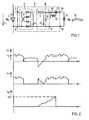
- the thyristor 1 shows a thyristor to be monitored, which can be arranged, for example, together with further thyristors in a valve branch of a converter arrangement.
- the thyristor 1 can be an electrically ignitable or, as shown in FIG. 1, a light-ignitable thyristor.
- Parallel to the thyristor 1 is a signaling device 2, which is connected with its input connections 3 to the anode connection or the cathode connection of the thyristor 1.
- the signaling device 2 contains a rectifier arrangement 4, which consists of four diodes 5 arranged to form a full-wave rectifier.
- the rectifier arrangement 4 is connected on the input side to the input connections 3 of the signaling device 2 and is connected on the output side to a downstream integrating element 6.
- the integrator 6 consists of a resistor 7 and a storage capacitor 8 connected in series therewith, the connections of which form the output 9 of the integrator 6.
- a threshold voltage switch 11 is arranged in a longitudinal branch. In the illustrated embodiment of the circuit arrangement according to the invention, this forms a toggle voltage switch and consists of an auxiliary thyristor 12, between the anode connection and gate connection of which there is a zener diode 13.
- the threshold voltage of the threshold voltage switch 11 corresponds to the zener voltage of its zener diode 13.
- the threshold voltage switch can also consist of a breakover diode, a unijunction thyristor or just a simple zener diode.
- a light-emitting diode 14 is connected to the output 10 of the signaling device 2, which can be an infrared light-emitting diode, for example.
- the light-emitting diode 14 is optically coupled to a line end of a light guide 15 shown only in sections here, the other line end of the light guide 15 being connected to an evaluation device (not shown).
- the course of the voltage u T at the thyristor 1, the current i T through the thyristor 1, the voltage u 1 at the output of the rectifier arrangement 4 and the Voltage Uc at the output 9 of the integrator 6 is shown depending on the time t.
- the curves of the voltages and the current shown result in the event that the thyristor shown in FIG. 1 forms a valve element of a converter system (not shown here) which operates in inverter operation.
- the current i T flows through the thyristor 1 and the value of the voltage u T applied to it is almost zero.
- the voltages u 1 at the output of the rectifier arrangement 4 and u c at the output 9 of the integrating element 6 each have the value zero, so that no current flows through the light-emitting diode 14.
- the voltage u T across the thyristor 1 assumes a voltage profile which differs from zero until the voltage of the positive voltage u T in the forward direction of the thyristor 1 is ignited and changes back into a current-conducting state.
- the voltage u l arises at the output of the rectifier arrangement 4 by rectifying the voltage u T.
- the voltage u l charges the capacitor 8 of the integrating element 6 via its resistance.
- the storage capacitor 8 is dimensioned such that its charging time until the voltage u c at the storage capacitor 8 reaches the value of the zener voltage Uz of the zener diode 13 corresponds to approximately one third to half the period of the alternating voltage with which the converter system is operated which the thyristor 1 is arranged.
- the voltage Uc at the storage capacitor 8 reaches the value of the Zener voltage Uz of the Zener diode 13
- This causes the auxiliary thyristor 12 to ignite.
- the storage capacitor 8 now discharges via the auxiliary thyristor 12 and the light-emitting diode 14, a very high, pulsed discharge current flowing.
- the high discharge current is converted into a light signal with a correspondingly high light output.
- the resistor 7 of the integrating element 6 is dimensioned such that after the storage capacitor 8 is discharged while the thyristor 1 is not in the conductive state, a residual current flows through the auxiliary thyristor 12 which is greater than the minimum value of the threshold voltage switch 11 corresponding to the holding current of the auxiliary thyristor 12. This prevents the auxiliary thyristor 12 from blocking during the ongoing non-conductive state of the thyristor 1 and the capacitor 8 being recharged and discharged again via the light-emitting diode 14.
Landscapes
- Engineering & Computer Science (AREA)
- Power Engineering (AREA)
- Power Conversion In General (AREA)
- Electronic Switches (AREA)
- Testing Of Individual Semiconductor Devices (AREA)
Abstract
Description
- Die Erfindung betrifft eine Schaltungsanordnung zur Überwachung eines Thyristors mit einer Signalgebervorrichtung, die eingangsseitig parallel zu dem Thyristor liegt und an deren Ausgang eine Leuchtdiode zur Aussendung von Lichtsignalen an eine Auswerteeinrichtung angeschlossen ist.
- Eine derartige Schaltungsanordnung ist in der "etz", Heft 25, Band 102, Dezember 1981, auf Seite 1341 f in Bild 7 dargestellt. Die bekannte Schaltungsanordnung ist Bestandteil einer Thyristorabschnittselektronik, die einem Thyristor zugeordnet ist. Die Thyristorabschnittselektronik weist zu ihrer Stromversorgung eine eigene Energieversorgungsschaltung auf und wird über diese aus einer Hilfsenergieauskoppelschaltung gespeist, die in Reihe mit einem Bedämpfungswiderstand und einem Bedämpfungskondensator parallel zu dem Thyristor liegt. Zur Überwachung des Thyristors enthält die Thyristorabschnittselektronik eine Signalgebervorrichtung mit einem parallel zu dem Thyristor liegenden ohmschen Spannungsteiler, an dessen Teilerabgriff eine Signalverarbeitungsschaltung angeschlossen ist; der Signalverarbeitungsschaltung ist ein Lichtsignalsender mit einer Leuchtdiode nachgeordnet, die bei Ansteuerung Lichtsignale aussendet. Die Lichtsignale werden über einen Lichtleiter an eine Auswerteeinrichtung übertragen.
- Der Erfindung liegt die Aufgabe zugrunde, eine Schaltungsanordnung zur Überwachung eines Thyristors anzugeben, die wegen Verzichts auf eine eigene Energieversorgungsschaltung besonders einfach und damit funktionssicher aufgebaut ist und eine Aussendung von Lichtsignalen mit besonders hoher Lichtleistung ermöglicht.
- Zur Lösung dieser Aufgabe enthält die Signalgebervorrichtung der eingangs angegebenen Art erfindungsgemäß eingangsseitig eine Gleichrichteranordnung, der ein Integrierglied nachgeordnet ist; zwischen dem Ausgang des Integriergliedes und dem Ausgang der Signalgebervorrichtung liegt ein Schwellenspannungsschalter, der in einen stromleitenden Zustand übergeht, sobald die an ihm abfallende Spannung einen vorgegebenen Schwellenwert überschreitet.
- Die Überwachung des Thyristors erfolgt durch Aussendung eines Lichtsignales an die Auswerteeinrichtung, wenn der Thyristor in den nichtleitenden Betriebszustand (Sperren, Blockieren) übergeht. Dabei besteht der wesentliche Vorteil der erfindungsgemäßen Schaltungsanordnung darin, daß im nichtleitenden Betriebszustand des Thyristors die Energie der an dem Thyristor entstehenden Spannung genutzt wird, um die Leuchtdiode zur Aussendung eines Lichtsignales anzusteuern; die Energie der Spannung am Thyristor wird dabei über die Gleichrichteranordnung, das Integrierglied und den Schwellenspannungsschalter der Leuchtdiode zugeführt. Eine eigene Energieversorgungsschaltung zur Stromversorgung der erfindungsgemäßen Schaltungsanordnung ist daher nicht erforderlich. Durch die direkte Ausnutzung der Energie der Spannung an dem Thyristor lassen sich in der Leuchtdiode Lichtsignale mit besonders hoher Lichtleistung erzeugen, so daß auch kostengünstigere, mit relativ hoher Dämpfung behaftete Lichtleiter Verwendung finden können, um die Lichtsignale dennoch sicher von der Leuchtdiode zu der Auswerteeinrichtung zu übertragen.
- Das Integrierglied bewirkt zusammen mit dem Schwellenspannungsschalter in vorteilhafter Weise, daß eine Ansteuerung der Leuchtdiode bei zufällig an dem Thyristor auftretenden Spannungssprüngen nicht erfolgt, weil erst dann eine Ansteuerung der Leuchtdiode erfolgt, wenn die Spannung am Ausgang des Integriergliedes den vorgegebenen Schwellenwert des Schwellenspannungsschalters überschreitet.
- Eine besonders hohe Lichtleistung der von der Leuchtdiode ausgesandten Lichtsignale wird dadurch erzielt, daß das Integrierglied aus einem Widerstand und einem mit diesem in Reihe liegenden Speicherkondensator besteht, dessen Anschlüsse den Ausgang des Integriergliedes bilden. Überschreitet nämlich die Spannung an dem Speicherkondensator den vorgegebenen Schwellenwert des Schwellenspannungsschalters, so steht die gesamte in dem Speicherkondensator gespeicherte Energie zur Verfügung, um einen hohen Entladestrom durch die Leuchtdiode zur Erzeugung eines Lichtsignales mit hoher Lichtleistung zu bewirken.
- Der Thyristor ist im allgemeinen in einer mit Wechselspannung betriebenen Anlage angeordnet; dabei ist es von Vorteil, wenn der Speicherkondensator und der Widerstand des Integriergliedes derart bemessen sind, daß die Ladezeit zur Aufladung des Speicherkondensators auf eine dem vorgegebenen Schwellenwert entsprechende Spannung einem Drittel bis der Hälfte der Periodendauer der Wechselspannung entspricht. Auf diese Weise erhält man eine bei nichtleitendem Thyristor gegenüber Spannungssprüngen an dem Thyristor unempfindliche Signalgebervorrichtung, wodurch eine fehlerhafte Ansteuerung der Leuchtdiode verhindert wird.
- Bei einer vorteilhaften Ausbildung der erfindungsgemäßen Schaltungsanordnung ist der Schwellenspannungsschalter ein Kippspannungsschalter, der erst dann von einem stromleitenden in einen stromsperrenden Zustand übergeht, wenn der durch ihn fließende Strom einen Mindestwert unterschreitet.
- Besonders vorteilhaft ist es, wenn der Widerstand des Integriergliedes derart bemessen ist, daß bei nichtleitendem Thyristor der Strom durch den Schwellenspannungsschalter größer als der vorgegebene Mindestwert ist. Dadurch wird nach der Aussendung eines Lichtsignales eine Aussendung weiterer Lichtsignale verhindert, solange der Thyristor noch nichtleitend ist. Erst wenn der Thyristor wieder in einen stromleitenden Zustand übergeht, sinkt der Strom durch den Schwellenspannungsschalter unter den vorgegebenen Mindestwert, so daß der Schwellenspannungsschalter wieder in einen stromsperrenden Zustand kippt.
- Zur Erläuterung der Erfindung ist in
- Fig. l ein bevorzugtes Ausführungsbeispiel der erfindungsgemäßen Schaltungsanordnung dargestellt;
- Fig. 2 zeigt ein Diagramm mit dem jeweiligen Verlauf der in Fig. 1 bezeichneten Spannungen und des in Fig. 1 bezeichneten Stromes.
- Fig. 1 zeigt einen zu überwachenden Thyristor, der beispielsweise zusammen mit weiteren Thyristoren in einem Ventilzweig einer Stromrichteranordnung angeordnet sein kann. Der Thyristor 1 kann ein elektrisch zündbarer oder entsprechend der Darstellung in Fig. 1 ein lichtzündbarer Thyristor sein. Parallel zu dem Thyristor 1 liegt eine Signalgebervorrichtung 2, die mit ihren Eingangsanschlüssen 3 an dem Anodenanschluß bzw. dem Kathodenanschluß des Thyristors 1 angeschlossen ist. Die Signalgebervorrichtung 2 enthält eine Gleichrichteranordnung 4, die aus vier zu einem Vollweggleichrichter angeordneten Dioden 5 besteht. Die Gleichrichteranordnung 4 ist eingangsseitig an den EingangsAnschlüssen 3 der Signalgebervorrichtung 2 angeschlossen und ausgangsseitig mit einem nachgeordneten Integrierglied 6 verbunden. Das Integrierglied 6 besteht aus einem Widerstand 7 und einem mit diesem in Reihe liegenden Speicherkondensator 8, dessen Anschlüsse den Ausgang 9 des Integriergliedes 6 bilden. Zwischen dem Ausgang 9 des Integriergliedes 6 und dem Ausgang 10 der Signalgebervorrichtung 2 ist in einem Längszweig ein Schwellenspannungsschalter 11 angeordnet. Dieser bildet bei dem dargestellten Ausführungsbeispiel der erfindungsgemäßen Schaltungsanordnung einen Kippspannungsschalter und besteht aus einem Hilfsthyristor 12, zwischen dessen Anodenanschluß und Gateanschluß eine Zenerdiode 13 liegt. Die Schwellenspannung des Schwellenspannungsschalters 11 entspricht der Zenerspannung seiner Zenerdiode 13. In Abwandlung zu dem dargestellten Ausführungsbeispiel kann der Schwellenspannungsschalter auch aus einer Kippspannungsdiode (Break-Over-Diode), einem Unijunctionthyristor oder lediglich aus einer einfachen Zenerdiode bestehen. An dem Ausgang 10 der Signalgebervorrichtung 2 ist eine Leuchtdiode 14 angeschlossen, die beispielsweise eine Infrarotleuchtdiode sein kann. Die Leuchtdiode 14 ist an einem Leitungsende eines hier nur abschnittsweise dargestellten Lichtleiters 15 optisch angekoppelt, wobei das andere Leitungsende des Lichtleiters 15 an einer nicht dargestellten Auswerteeinrichtung angeschlossen ist.
- Zur Erläuterung der Funktionsweise des in Fig. 1 dargestellten Ausführungsbeispieles der erfindungsgemäßen Schaltungsanordnung sind in Fig. 2 der Verlauf der Spannung uT an dem Thyristor 1, der Strom iT durch den Thyristor 1, die Spannung u1 am Ausgang der Gleichrichteranordnung 4 und die Spannung Uc am Ausgang 9 des Integriergliedes 6 jeweils in Abhängigkeit von der Zeit t dargestellt. Die gezeigten Verläufe der Spannungen und des Stromes ergeben sich für den Fall, daß der in Fig. 1 dargestellte Thyristor ein Ventilelement einer hier nicht dargestellten, im Wechselrichterbetrieb arbeitenden Stromrichteranlage bildet. Solange sich der Thyristor 1 in einem stromleitenden Zustand befindet, fließt der Strom iT durch den Thyristor 1 und der Wert der an ihm anliegenden Spannung uT ist nahezu Null. Dementsprechend weisen auch die Spannungen u1 am Ausgang der Gleichrichteranordnung 4 und uc am Ausgang 9 des Integriergliedes 6 jeweils den Wert Null auf, so daß kein Strom durch die Leuchtdiode 14 fließt. Sobald der Thyristor 1 in einen sperrenden Zustand übergeht, nimmt die Spannung uT an dem Thyristor 1 einen von Null verschiedenen Spannungsverlauf an, bis bei positiver Spannung uT in Durchlaßrichtung des Thyristors 1 dieser gezündet wird und wieder in einen stromleitenden Zustand übergeht. Während des nichtleitenden Zustandes des Thyristors 1 entsteht am Ausgang der Gleichrichteranordnung 4 durch Gleichrichtung der Spannung uT die Spannung ul. Die Spannung ul lädt den Kondensator 8 des Integriergliedes 6 über dessen Widerstand auf. Der Speicherkondensator 8 ist derart dimensioniert, daß seine Ladezeit, bis die Spannung uc an dem Speicherkondensator 8 den Wert der Zenerspannung Uz der Zenerdiode 13 erreicht, etwa einem Drittel bis der Hälfte der Periodendauer der Wechselspannung entspricht, mit der die Stromrichteranlage betrieben wird, in der der Thyristor 1 angeordnet ist. Sobald die Spannung Uc an dem Speicherkonoensator 8 den Wert der Zenerspannung Uz der Zenerdiode 13 erreicht, bewirkt dieser eine Zündung des Hilfsthyristors 12. Der Speicherkondensator 8 entlädt sich nun über den Hilfsthyristor 12 und die Leuchtdiode 14, wobei ein sehr hoher, impulsförmiger Entladestrom fließt. In der Leuchtdiode 14 wird der hohe Entladestrom in ein Lichtsignal mit entsprechend hoher Lichtleistung umgewandelt. Der Widerstand 7 des Integriergliedes 6 ist derart bemessen, daß nach der Entladung des Speicherkondensators 8 während des nichtleitenden Zustandes des Thyristors 1 ein Reststrom durch den Hilfsthyristor 12 fließt, der größer als der dem Haltestrom des Hilfsthyristors 12 entsprechende Mindestwert des Schwellenspannungsschalters 11 ist. Dadurch wird verhindert, daß der Hilfsthyristor 12 während des andauernden nichtleitenden Zustandes des Thyristors 1 sperrt und der Kondensator 8 erneut aufgeladen und über die Leuchtdiode 14 wieder entladen wird.
Claims (5)
Priority Applications (1)
| Application Number | Priority Date | Filing Date | Title |
|---|---|---|---|
| AT85108229T ATE37637T1 (de) | 1984-07-17 | 1985-07-03 | Schaltungsanordnung zur ueberwachung eines thyristors. |
Applications Claiming Priority (2)
| Application Number | Priority Date | Filing Date | Title |
|---|---|---|---|
| DE3426767 | 1984-07-17 | ||
| DE19843426767 DE3426767A1 (de) | 1984-07-17 | 1984-07-17 | Schaltungsanordnung zur ueberwachung eines thyristors |
Publications (2)
| Publication Number | Publication Date |
|---|---|
| EP0168715A1 true EP0168715A1 (de) | 1986-01-22 |
| EP0168715B1 EP0168715B1 (de) | 1988-09-28 |
Family
ID=6241132
Family Applications (1)
| Application Number | Title | Priority Date | Filing Date |
|---|---|---|---|
| EP85108229A Expired EP0168715B1 (de) | 1984-07-17 | 1985-07-03 | Schaltungsanordnung zur Überwachung eines Thyristors |
Country Status (9)
| Country | Link |
|---|---|
| US (1) | US4675542A (de) |
| EP (1) | EP0168715B1 (de) |
| JP (1) | JPS6139850A (de) |
| AT (1) | ATE37637T1 (de) |
| BR (1) | BR8503372A (de) |
| CA (1) | CA1235745A (de) |
| DE (2) | DE3426767A1 (de) |
| DK (1) | DK322685A (de) |
| IN (1) | IN162966B (de) |
Cited By (1)
| Publication number | Priority date | Publication date | Assignee | Title |
|---|---|---|---|---|
| CN102361393A (zh) * | 2011-11-11 | 2012-02-22 | 江苏正佰电气有限公司 | 直流电源柜 |
Families Citing this family (5)
| Publication number | Priority date | Publication date | Assignee | Title |
|---|---|---|---|---|
| DE3601282A1 (de) * | 1986-01-17 | 1987-07-23 | Hoermann Gmbh | Schaltungsanordnung zur spannungsueberwachung |
| DE3722489C1 (en) * | 1987-07-04 | 1988-09-29 | Licentia Gmbh | Circuit arrangement for status indication of thyristors in a high voltage valve |
| DE4300620C1 (de) * | 1993-01-13 | 1994-07-14 | Systemtechnik Leber | Verfahren zur Überwachung des Stromflusses durch einen elektrischen Schalter |
| DE19532633A1 (de) * | 1995-08-22 | 1997-02-27 | Fahrzeugausruestung Berlin Gmb | Schaltungsanordnung zur Überwachung der Sperrfähigkeit in Reihe geschalteter elektronischer Schaltelemente |
| CN109239564B (zh) * | 2017-07-10 | 2021-02-26 | 南京南瑞继保电气有限公司 | 一种基于软件逻辑功能配合的晶闸管测试系统 |
Citations (1)
| Publication number | Priority date | Publication date | Assignee | Title |
|---|---|---|---|---|
| DE2363617A1 (de) * | 1973-12-20 | 1975-06-26 | Siemens Ag | Einrichtung zur steuerung eines thyristors |
Family Cites Families (4)
| Publication number | Priority date | Publication date | Assignee | Title |
|---|---|---|---|---|
| DE2360173A1 (de) * | 1973-12-03 | 1975-06-19 | Siemens Ag | Schaltungsanordnung zur zuendung eines elektrischen ventils, insbesondere eines thyristors |
| US4151427A (en) * | 1977-07-15 | 1979-04-24 | Travin Lev V | High-voltage zero-crossing detector |
| US4229669A (en) * | 1978-04-03 | 1980-10-21 | International Business Machines Corporation | Tight tolerance zero crossing detector circuit |
| JPS5932319A (ja) * | 1982-08-13 | 1984-02-21 | 富士電機株式会社 | サイリスタスイツチ故障監視方式 |
-
1984
- 1984-07-17 DE DE19843426767 patent/DE3426767A1/de not_active Withdrawn
-
1985
- 1985-06-06 IN IN429/CAL/85A patent/IN162966B/en unknown
- 1985-06-10 US US06/742,804 patent/US4675542A/en not_active Expired - Fee Related
- 1985-06-14 CA CA000483967A patent/CA1235745A/en not_active Expired
- 1985-07-03 EP EP85108229A patent/EP0168715B1/de not_active Expired
- 1985-07-03 DE DE8585108229T patent/DE3565348D1/de not_active Expired
- 1985-07-03 AT AT85108229T patent/ATE37637T1/de not_active IP Right Cessation
- 1985-07-16 BR BR8503372A patent/BR8503372A/pt unknown
- 1985-07-16 DK DK322685A patent/DK322685A/da not_active Application Discontinuation
- 1985-07-16 JP JP15686885A patent/JPS6139850A/ja active Pending
Patent Citations (1)
| Publication number | Priority date | Publication date | Assignee | Title |
|---|---|---|---|---|
| DE2363617A1 (de) * | 1973-12-20 | 1975-06-26 | Siemens Ag | Einrichtung zur steuerung eines thyristors |
Cited By (1)
| Publication number | Priority date | Publication date | Assignee | Title |
|---|---|---|---|---|
| CN102361393A (zh) * | 2011-11-11 | 2012-02-22 | 江苏正佰电气有限公司 | 直流电源柜 |
Also Published As
| Publication number | Publication date |
|---|---|
| DK322685D0 (da) | 1985-07-16 |
| CA1235745A (en) | 1988-04-26 |
| IN162966B (de) | 1988-07-30 |
| EP0168715B1 (de) | 1988-09-28 |
| DE3565348D1 (en) | 1988-11-03 |
| US4675542A (en) | 1987-06-23 |
| JPS6139850A (ja) | 1986-02-26 |
| DK322685A (da) | 1986-01-18 |
| ATE37637T1 (de) | 1988-10-15 |
| BR8503372A (pt) | 1986-04-08 |
| DE3426767A1 (de) | 1986-01-23 |
Similar Documents
| Publication | Publication Date | Title |
|---|---|---|
| DE2457664C2 (de) | Elektrische Schaltungsanordnung zur Erzeugung einer stabilen Ausgangsspannung | |
| EP0168715B1 (de) | Schaltungsanordnung zur Überwachung eines Thyristors | |
| DE2103922C3 (de) | Schaltungsanordnung zum Schnelladen einer elektrischen Akkumulatoren-Batterie | |
| DE2838435C2 (de) | ||
| DE3033916C2 (de) | ||
| DE3019071C2 (de) | ||
| EP0170882A1 (de) | Schaltungsanordnung zur Überwachung eines Thyristors | |
| US3333120A (en) | Pulse forming network voltage regulator | |
| DE3426769A1 (de) | Schaltungsanordnung zur ueberwachung eines thyristors | |
| DE3437953C2 (de) | ||
| DE1211096B (de) | Elektrische Zuendvorrichtung | |
| DE4026461C2 (de) | ||
| CH539297A (de) | Gleichspannungswandler zur Erzeugung einer stabilisierten, von einer Quelle schwankender Zuliefer-Gleichspannung galvanisch getrennten, an Verbraucher abzugebenden Gleichspannung | |
| EP0062288B1 (de) | Direkt an ein Wechselspannungsnetz anschliessbare Wechsellichtschranke | |
| DE3426768A1 (de) | Schaltungsanordnung zum betrieb von thyristoren in einem ventilzweig | |
| DE2743913A1 (de) | Schaltungsanordnung fuer ein photo- blitzlichtgeraet | |
| DE1765552A1 (de) | Schaltungsanordnung zur Funkenerosion | |
| DE917375C (de) | Schaltungsanordnung fuer Wechselstromerzeuger, insbesondere Polwechsler in Fernsprechanlagen | |
| DE2250646C2 (de) | Schaltungsanordnung zur Erzeugung elektrischer Einzelimpulse großer Leistung | |
| DE2401596C3 (de) | Eintakt-Gleichspannungswandler zur Impulssteuerung der Spannung an einer induktiven Last sowie Verfahren zu seinem Betrieb | |
| DE3720701C2 (de) | ||
| DE1413752C (de) | Schaltungsanordnung zur Steuerung der Drehzahl von Elektromotoren | |
| DE1413450C (de) | Zundschaltungsanordnung | |
| AT339995B (de) | Kondensatorzundmaschine | |
| DE1763900C3 (de) | Fremdgesteuerter Gleichspannungswandler |
Legal Events
| Date | Code | Title | Description |
|---|---|---|---|
| PUAI | Public reference made under article 153(3) epc to a published international application that has entered the european phase |
Free format text: ORIGINAL CODE: 0009012 |
|
| AK | Designated contracting states |
Designated state(s): AT CH DE FR GB IT LI SE |
|
| 17P | Request for examination filed |
Effective date: 19860226 |
|
| 17Q | First examination report despatched |
Effective date: 19861209 |
|
| D17Q | First examination report despatched (deleted) | ||
| GRAA | (expected) grant |
Free format text: ORIGINAL CODE: 0009210 |
|
| AK | Designated contracting states |
Kind code of ref document: B1 Designated state(s): AT CH DE FR GB IT LI SE |
|
| REF | Corresponds to: |
Ref document number: 37637 Country of ref document: AT Date of ref document: 19881015 Kind code of ref document: T |
|
| REF | Corresponds to: |
Ref document number: 3565348 Country of ref document: DE Date of ref document: 19881103 |
|
| ET | Fr: translation filed | ||
| ITF | It: translation for a ep patent filed | ||
| GBT | Gb: translation of ep patent filed (gb section 77(6)(a)/1977) | ||
| PLBE | No opposition filed within time limit |
Free format text: ORIGINAL CODE: 0009261 |
|
| STAA | Information on the status of an ep patent application or granted ep patent |
Free format text: STATUS: NO OPPOSITION FILED WITHIN TIME LIMIT |
|
| 26N | No opposition filed | ||
| PGFP | Annual fee paid to national office [announced via postgrant information from national office to epo] |
Ref country code: GB Payment date: 19910625 Year of fee payment: 7 |
|
| PGFP | Annual fee paid to national office [announced via postgrant information from national office to epo] |
Ref country code: AT Payment date: 19910628 Year of fee payment: 7 |
|
| PGFP | Annual fee paid to national office [announced via postgrant information from national office to epo] |
Ref country code: FR Payment date: 19910718 Year of fee payment: 7 |
|
| ITTA | It: last paid annual fee | ||
| PGFP | Annual fee paid to national office [announced via postgrant information from national office to epo] |
Ref country code: SE Payment date: 19910731 Year of fee payment: 7 |
|
| PGFP | Annual fee paid to national office [announced via postgrant information from national office to epo] |
Ref country code: DE Payment date: 19910917 Year of fee payment: 7 |
|
| PGFP | Annual fee paid to national office [announced via postgrant information from national office to epo] |
Ref country code: CH Payment date: 19911030 Year of fee payment: 7 |
|
| PG25 | Lapsed in a contracting state [announced via postgrant information from national office to epo] |
Ref country code: GB Effective date: 19920703 Ref country code: AT Effective date: 19920703 |
|
| PG25 | Lapsed in a contracting state [announced via postgrant information from national office to epo] |
Ref country code: SE Effective date: 19920704 |
|
| PG25 | Lapsed in a contracting state [announced via postgrant information from national office to epo] |
Ref country code: LI Effective date: 19920731 Ref country code: CH Effective date: 19920731 |
|
| GBPC | Gb: european patent ceased through non-payment of renewal fee |
Effective date: 19920703 |
|
| PG25 | Lapsed in a contracting state [announced via postgrant information from national office to epo] |
Ref country code: FR Effective date: 19930331 |
|
| REG | Reference to a national code |
Ref country code: CH Ref legal event code: PL |
|
| PG25 | Lapsed in a contracting state [announced via postgrant information from national office to epo] |
Ref country code: DE Effective date: 19930401 |
|
| REG | Reference to a national code |
Ref country code: FR Ref legal event code: ST |
|
| EUG | Se: european patent has lapsed |
Ref document number: 85108229.7 Effective date: 19930204 |