EP0169064A2 - Tintenstrahlantrieb gekoppelt mit einem Niederspannungstransformator - Google Patents
Tintenstrahlantrieb gekoppelt mit einem Niederspannungstransformator Download PDFInfo
- Publication number
- EP0169064A2 EP0169064A2 EP85305102A EP85305102A EP0169064A2 EP 0169064 A2 EP0169064 A2 EP 0169064A2 EP 85305102 A EP85305102 A EP 85305102A EP 85305102 A EP85305102 A EP 85305102A EP 0169064 A2 EP0169064 A2 EP 0169064A2
- Authority
- EP
- European Patent Office
- Prior art keywords
- ink jet
- pzt
- low voltage
- circuit
- signal
- Prior art date
- Legal status (The legal status is an assumption and is not a legal conclusion. Google has not performed a legal analysis and makes no representation as to the accuracy of the status listed.)
- Granted
Links
Images
Classifications
-
- B—PERFORMING OPERATIONS; TRANSPORTING
- B41—PRINTING; LINING MACHINES; TYPEWRITERS; STAMPS
- B41J—TYPEWRITERS; SELECTIVE PRINTING MECHANISMS, i.e. MECHANISMS PRINTING OTHERWISE THAN FROM A FORME; CORRECTION OF TYPOGRAPHICAL ERRORS
- B41J2/00—Typewriters or selective printing mechanisms characterised by the printing or marking process for which they are designed
- B41J2/005—Typewriters or selective printing mechanisms characterised by the printing or marking process for which they are designed characterised by bringing liquid or particles selectively into contact with a printing material
- B41J2/01—Ink jet
- B41J2/015—Ink jet characterised by the jet generation process
- B41J2/04—Ink jet characterised by the jet generation process generating single droplets or particles on demand
- B41J2/045—Ink jet characterised by the jet generation process generating single droplets or particles on demand by pressure, e.g. electromechanical transducers
- B41J2/04501—Control methods or devices therefor, e.g. driver circuits, control circuits
- B41J2/0452—Control methods or devices therefor, e.g. driver circuits, control circuits reducing demand in current or voltage
-
- B—PERFORMING OPERATIONS; TRANSPORTING
- B41—PRINTING; LINING MACHINES; TYPEWRITERS; STAMPS
- B41J—TYPEWRITERS; SELECTIVE PRINTING MECHANISMS, i.e. MECHANISMS PRINTING OTHERWISE THAN FROM A FORME; CORRECTION OF TYPOGRAPHICAL ERRORS
- B41J2/00—Typewriters or selective printing mechanisms characterised by the printing or marking process for which they are designed
- B41J2/005—Typewriters or selective printing mechanisms characterised by the printing or marking process for which they are designed characterised by bringing liquid or particles selectively into contact with a printing material
- B41J2/01—Ink jet
- B41J2/015—Ink jet characterised by the jet generation process
- B41J2/04—Ink jet characterised by the jet generation process generating single droplets or particles on demand
- B41J2/045—Ink jet characterised by the jet generation process generating single droplets or particles on demand by pressure, e.g. electromechanical transducers
- B41J2/04501—Control methods or devices therefor, e.g. driver circuits, control circuits
- B41J2/04541—Specific driving circuit
-
- B—PERFORMING OPERATIONS; TRANSPORTING
- B41—PRINTING; LINING MACHINES; TYPEWRITERS; STAMPS
- B41J—TYPEWRITERS; SELECTIVE PRINTING MECHANISMS, i.e. MECHANISMS PRINTING OTHERWISE THAN FROM A FORME; CORRECTION OF TYPOGRAPHICAL ERRORS
- B41J2/00—Typewriters or selective printing mechanisms characterised by the printing or marking process for which they are designed
- B41J2/005—Typewriters or selective printing mechanisms characterised by the printing or marking process for which they are designed characterised by bringing liquid or particles selectively into contact with a printing material
- B41J2/01—Ink jet
- B41J2/015—Ink jet characterised by the jet generation process
- B41J2/04—Ink jet characterised by the jet generation process generating single droplets or particles on demand
- B41J2/045—Ink jet characterised by the jet generation process generating single droplets or particles on demand by pressure, e.g. electromechanical transducers
- B41J2/04501—Control methods or devices therefor, e.g. driver circuits, control circuits
- B41J2/04581—Control methods or devices therefor, e.g. driver circuits, control circuits controlling heads based on piezoelectric elements
Definitions
- the present invention relates to ink jet printers, and more particularly to the driver for a piezoelectric crystal ink jet.
- the typical driver for piezoelectric (PZT) crystal ink jets in the prior art consists of a linear high voltage amplifier which is generally D.C. coupled.
- An ink jet driver which uses a low cost, low power monolithic power amplifier with the higher voltages of the PZT only in the final stage is desirable.
- the present invention provides such a PZT driver.
- the present invention provides a low voltage PZT ink jet driver circuit for developing a high voltage PZT excitation signal in response to a low voltage video fsignal.
- the driver includes a power gain stage which is coupled to receive the low voltage video signal for amplifying that signal into a signal having a voltage level intermediate that of the input video signal and the necessary PZT excitation signal. Coupled to the output of the power gain stage is a serially connected capacitor-resistor network which in turn is coupled to the primary winding of a transformer means for stepping-up the video signal from the intermediate voltage level to the selected PZT excitation voltage across the secondary winding of the transformer means.
- the inductance of the secondary winding is matched to the average capacitance of the type of PZT ink jet selected to form a parallel resonant circuit therewith which has a resonant frequency at the selected droplet printing frequency.
- the characteristics of the primary winding of the transformer means are set by the number of turns used in the secondary winding and the necessary turns ratio to obtain the desired voltage level in the excitation signal from the intermediate voltage levels of the video signal.
- the capacitor-resistor network and the primary winding form a series resonant circuit with the value of the capacitor selected to produce a resonant frequency that is substantially lower than the droplet frequency.
- the value of the resistor in the series resonant circuit is selected to minimize its Q and to critically damp or overdamp the series resonant circuit.
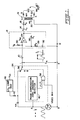
- Fig. 1 is a schematic diagram of the PZT driver of the present invention.
- the image is printed a droplet, or dot, at a time, at a high frequency rate.
- a typical droplet printing rate is approximately 20 KHz.
- a properly designed driver must have the ability to turn the PZT ink jet on and off accurately, witheut printing too many or too few dots each time the driver is activated.
- the signal which is applied to the driver may, for example, be a video signal that corresponds to a selected and stored image of a storage monitor.
- the video signal represents a string of the pixels of that image arranged in sequential lines across the face of the monitor as a composite of the individual pixel signals.
- Each pixel signal depending on the resolution of the monitor, the brightness of that pixel in the image and the ink jet printer droplet size, triggers the release from the ink jet of one or more droplets of ink.
- each pixel signal portion of that signal consists of a "return to zero" signal. That is, each pixel signal starts at zero volts or at a zero voltage crossing point, and ends at zero volts or at a later zero voltage crossing point, e.g. a sine wave.
- each pixel signal starts at zero volts or at a zero voltage crossing point, and ends at zero volts or at a later zero voltage crossing point, e.g. a sine wave.
- a low voltage power gain stage 12 which is transformer 18 coupled to the PZT ink jet. Also shown is a capacitor 10 coupled serially between the driver input terminal 1 and the non-inverting input terminal of gain stage 12.
- Gain stage 12 includes gain setting resistors 26 and 28, having values of R, and R 2 respectively, and a power amplifier 24 which may be implemented by a monolithic power amplifier (e.g. SGS TDA 2030A).
- the output terminal of gain stage 12 is -- f onnected serially to a second capacitor 14 (C c ), resistor 16 (R s )r and then to the primary winding 20 of transformer 18 (T 1 ). The other end of the primary winding is then connected to the return line which is also input terminal 2.
- the ends of the secondary winding 22 of transformer 18 are connected to output terminals 3 and 4 which are disposed to couple with the PZT ink jet.
- the voltage gain of the circuit shown in Fig. 1 is a combination of the gain of gain stage 12 and transformer 18. That gain can be expressed as follows: where N p is the number of turns of the primary winding 20 of transformer 18 and N is the number of turns of the secondary winding 22 of transformer 18.
- the circuit of Fig. 1 includes two resonant circuits when the PZT ink jet is coupled to output terminals 3 and 4.
- the first resonant circuit is a series RLC circuit which includes C c , R and the primary winding 20.
- the second resonant circuit is a parallel LC circuit which includes the secondary winding 22 and the PZT ink jet.
- the inductance of the secondary winding 22 should be matched to the capacitance of the PZT, so that the second resonant circuit resonates at the selected droplet frequency.
- the number of secondary turns necessary to produce that inductance on that core can be determined.
- the power factor is maximized and the load appears to be less'reactive and fmore real. By doing this, the load on the power amplifier is reduced with an overall power savings and a smaller thermal load on the power amplifier.
- the number of turns in the primary winding 20 is set by the turns ratio which is necessary to obtain the necessary voltage gain (see Equation 1).
- an excitation signal of 250-500 V p-p is necessary to cause the production of the ink droplets on demand.
- the necessary voltage gain in this example is 100, which is divided between power amplifier 24 and transformer 18.
- a gain of 7 was selected for the power amplifier 24 and a turns ratio of transformer 18 of 14.4.
- the first resonant circuit should be critically damped or overdamped, the Q of this circuit should be very low, and its resonant frequency should be lower and quite removed from the resonant frequency of the second resonant circuit.
- the first resonant circuit was designed to have a resonant frequency of approximately 50 Hz and a Q of 1.4 or less.
- the first resonant circuit includes capacitor 14 (C c ) and L (the inductance of primary winding 20) with resistor 16 (R s ) to control the Q of the circuit. It is necessary to control Q so that low frequency artifacts are not introduced into the printed output.
- the series damping resistor 16 also acts to swamp the effects of transformer leakage inductance which, if left unchecked, would degrade signal fidelity by introducing overshoot of the output signal at the termination of a droplet ejection cycle.
- __video information excites the ink jet in a burst having half period that is harmonically related to the period of the first resonant circuit, and that pattern repeats with an equal length off period between bursts (i.e. alternating N pixels on and N pixels off in the video image), and that the first resonant circuit has a high Q.
- the first resonant circuit will develop an alternating potential at its resonant period which will be algebraically added to the pixel video information of the input signal.
- resistor 16 in the first resonant circuit introduces a low frequency artifact equal to the video envelope period having a magnitude IR s , where I equals the current reflected at the transformer primary 20 transferred into or out of the second resonant circuit.
- the artifact will be algebraically added to the drive signal at the amplifier output and would compromise the performance and reliability of the ink jet.
- the IR s offset voltage is compensated for through pre-compensation of the reference waveform to generate E in .
- the pre-compensation circuit includes a synchronous waveform gate 34 coupled between terminal 1 and reference input terminals A and B with terminals A and B disposed to receive a reference signal, E ref' which has a frequency substantially equal to the frequency of the individual pixel signal of the video-in signal.
- the synchronous waveform gate 34 includes a phase 'compensation zero crossing detector 40 having its input terminal connected to terminal A.
- the output signal from detector 40 as shown here, consists of a square wave which changes state each time the signal Eref crosses the zero voltage potential.
- One input terminal of AND gate 38 is connected to the output terminal of detector 40, and the second input terminal of gate 38 is disposed to receive the video data signal, the representative image of which is to be printed by the ink jet.
- the output signal from gate 38 in turn controls a DPDT switch 36 which is shown here as a mechanical switch, however, it is obvious to anyone skilled in the art that it can be replaced with an electronic switch of any of several types.
- the common terminal of switch 36 is connected to terminal 1.
- the poles of switch 3E are connected to the return line of the circuit and terminal A via a coupling capacitor 44. Also connected to the pole of switch 36 associated with capacitor 44 is a power supply 46 via resistor 42.
- the polarity of the output voltage of power supply 46 is controlled by detector 40 such that a bias voltage of a polarity opposite to that of the IR s voltage drop and of an appropriate magnitude is added to Eref prior to the gating of E ref by switch 36 under the control of the pixel information content of the video-in signal.
- Reference pre-compensation is completed through phase shifting the waveform gate an appropriate amount (sine -1 (V bias /V peak reference )) such that the apparent waveform gating occurs at the zero crossing of the exitation signal of the ink jet.
- the segments of the input signal, E in were 2.5 V p-p at 20 KHz, and the output signal was 250 V p-p at 20 KHz.
- the individual circuit components had the selected values or designations shown in the following table:
- the transformers could be individually adjusted to match the capacitance of a selected PZT ink jet, the PZT ink jets could be screened to select ones that have a capacitance within a preset tolerance range to match the selected transformer de- - sign, or the transformer could be designed to match the average or median value of the capacitance of the available PZT ink jets which all have the other specified characteristics.
- the first two of these options are very time and cost intensive, which in the production of a general use instrument would not be acceptable.
Landscapes
- Particle Formation And Scattering Control In Inkjet Printers (AREA)
- Apparatuses For Generation Of Mechanical Vibrations (AREA)
Applications Claiming Priority (2)
| Application Number | Priority Date | Filing Date | Title |
|---|---|---|---|
| US06/631,969 US4560998A (en) | 1984-07-18 | 1984-07-18 | Low voltage transformer coupled ink jet driver |
| US631969 | 1996-04-15 |
Publications (3)
| Publication Number | Publication Date |
|---|---|
| EP0169064A2 true EP0169064A2 (de) | 1986-01-22 |
| EP0169064A3 EP0169064A3 (en) | 1986-09-17 |
| EP0169064B1 EP0169064B1 (de) | 1990-05-02 |
Family
ID=24533529
Family Applications (1)
| Application Number | Title | Priority Date | Filing Date |
|---|---|---|---|
| EP85305102A Expired EP0169064B1 (de) | 1984-07-18 | 1985-07-17 | Tintenstrahlantrieb gekoppelt mit einem Niederspannungstransformator |
Country Status (5)
| Country | Link |
|---|---|
| US (1) | US4560998A (de) |
| EP (1) | EP0169064B1 (de) |
| JP (1) | JPS6144653A (de) |
| CA (1) | CA1238239A (de) |
| DE (1) | DE3577417D1 (de) |
Cited By (1)
| Publication number | Priority date | Publication date | Assignee | Title |
|---|---|---|---|---|
| EP0200457A1 (de) * | 1985-05-02 | 1986-11-05 | Ing. C. Olivetti & C., S.p.A. | Steuerschaltung für ein Tintenstrahldruckelement und Verfahren, welches sich auf ihre Dimensionierung und Herstellung bezieht |
Families Citing this family (6)
| Publication number | Priority date | Publication date | Assignee | Title |
|---|---|---|---|---|
| US4749897A (en) * | 1986-03-12 | 1988-06-07 | Nippondenso Co., Ltd. | Driving device for piezoelectric element |
| DE4400210A1 (de) * | 1994-01-05 | 1995-08-10 | Branson Ultraschall | Verfahren und Einrichtung zum Betrieb eines Generators zur HF-Energieversorgung eines Ultraschallwandlers |
| US6068360A (en) * | 1997-06-30 | 2000-05-30 | Brother Kogyo Kabushiki Kaisha | Printer head drive system having negative feedback control |
| DE10134188A1 (de) * | 2001-07-13 | 2003-01-23 | Heidelberger Druckmasch Ag | Tintenstrahl-Drucksystem |
| US6817704B2 (en) * | 2002-08-20 | 2004-11-16 | Sony Corporation | Liquid ejecting device and liquid ejecting method |
| JP5436164B2 (ja) | 2009-11-20 | 2014-03-05 | キヤノン株式会社 | 振動型アクチュエータの駆動回路 |
Family Cites Families (11)
| Publication number | Priority date | Publication date | Assignee | Title |
|---|---|---|---|---|
| FR2123242A1 (de) * | 1971-01-25 | 1972-09-08 | Electro Mechanical Desig | |
| DE2363731C3 (de) * | 1973-12-21 | 1980-02-07 | Graetz Gmbh & Co Ohg, 5990 Altena | Akustische Anzeigevorrichtung |
| DE2548691C3 (de) * | 1975-10-30 | 1986-04-17 | Siemens AG, 1000 Berlin und 8000 München | Schaltungsanordnung zum Ansteuern von Schreibdüsen in Tintenmosaikschreibeinrichtungen |
| DE2629562C2 (de) * | 1976-07-01 | 1982-06-24 | Danfoss A/S, 6430 Nordborg | Gerät zur Ultraschallmessung |
| DE2850016C2 (de) * | 1978-11-17 | 1984-03-22 | Siemens AG, 1000 Berlin und 8000 München | Schaltungsanordnung zum Ansteuern von Schreibdüsen in Tintenmosaikschreibeinrichtungen |
| DE2903339C3 (de) * | 1979-01-29 | 1987-06-19 | Siemens AG, 1000 Berlin und 8000 München | Schaltungsanordnung zur temperaturabhängigen Spannungsregelung für piezoelektrische Schreibdüsen in Tintenmosaikschreibeinrichtungen |
| JPS55147786A (en) * | 1979-05-08 | 1980-11-17 | Seiko Epson Corp | Portable recorder |
| JPS57100080A (en) * | 1980-12-12 | 1982-06-22 | Matsushita Electric Ind Co Ltd | Color ink jet recorder |
| JPS57188369A (en) * | 1981-05-15 | 1982-11-19 | Hitachi Ltd | Ink jet recorder |
| JPS5845066A (ja) * | 1981-09-09 | 1983-03-16 | Matsushita Electric Ind Co Ltd | インクジエツト記録装置 |
| JPS5855253A (ja) * | 1981-09-29 | 1983-04-01 | Ricoh Co Ltd | インクジエツト記録装置における電歪振動子駆動方法 |
-
1984
- 1984-07-18 US US06/631,969 patent/US4560998A/en not_active Expired - Fee Related
-
1985
- 1985-06-27 CA CA000485538A patent/CA1238239A/en not_active Expired
- 1985-07-17 DE DE8585305102T patent/DE3577417D1/de not_active Expired - Fee Related
- 1985-07-17 JP JP60157972A patent/JPS6144653A/ja active Pending
- 1985-07-17 EP EP85305102A patent/EP0169064B1/de not_active Expired
Cited By (1)
| Publication number | Priority date | Publication date | Assignee | Title |
|---|---|---|---|---|
| EP0200457A1 (de) * | 1985-05-02 | 1986-11-05 | Ing. C. Olivetti & C., S.p.A. | Steuerschaltung für ein Tintenstrahldruckelement und Verfahren, welches sich auf ihre Dimensionierung und Herstellung bezieht |
Also Published As
| Publication number | Publication date |
|---|---|
| EP0169064A3 (en) | 1986-09-17 |
| JPS6144653A (ja) | 1986-03-04 |
| EP0169064B1 (de) | 1990-05-02 |
| DE3577417D1 (de) | 1990-06-07 |
| US4560998A (en) | 1985-12-24 |
| CA1238239A (en) | 1988-06-21 |
Similar Documents
| Publication | Publication Date | Title |
|---|---|---|
| US6759766B2 (en) | Power supply apparatus and image forming apparatus using the same | |
| US5991167A (en) | DC to DC power converter including synchronous output rectifier circuit | |
| US6582043B2 (en) | Driving device and driving method for ink jet printing head | |
| US4563689A (en) | Method for ink-jet recording and apparatus therefor | |
| DE69929735T2 (de) | Steuerschaltung eines Tintenstrahldruckkopfes | |
| US4560998A (en) | Low voltage transformer coupled ink jet driver | |
| AU612118B2 (en) | High voltage power supply particularly adapted for a TWT | |
| US20040169545A1 (en) | Capactive load driving circuit, capacitive load driving method, and apparatus using the same | |
| JPS60125672A (ja) | マルチヘッド液体噴射記録装置 | |
| GB2133186A (en) | Power supply for crt terminal | |
| EP0517116B1 (de) | Schaltung zur Hochspannungserzeugung | |
| KR19980064788A (ko) | 고전압발생회로 | |
| JPS6348713B2 (de) | ||
| DE4015461A1 (de) | Schaltung zum stabilisieren der hochspannung einer hochspannungsgeneratorschaltung einer kathodenstrahlroehre | |
| US10556425B2 (en) | Liquid discharge device and printing apparatus | |
| US6278470B1 (en) | Energy efficient RF generator for driving an electron beam print cartridge to print a moving substrate | |
| US20050259449A1 (en) | High voltage power supply | |
| JPS59104952A (ja) | ドツト式プリンタ制御装置 | |
| JPH0671938A (ja) | 画像形成装置 | |
| JP2001063040A (ja) | インクジェット記録装置 | |
| DE1514342C (de) | Ablenkschaltung zur magnetischen Ablenkung des Kathodenstrahls in fernsehtechnischen Geräten mit Linearitätskorrektur | |
| DE2338018C3 (de) | Anordnung zum Regeln der Tröpfchenfrequenz von Tintenstrahlschreiber!! | |
| JPH03159417A (ja) | 高圧パラボラ波発生装置 | |
| JP2025148701A (ja) | 画像形成装置 | |
| JPS6226914B2 (de) |
Legal Events
| Date | Code | Title | Description |
|---|---|---|---|
| PUAI | Public reference made under article 153(3) epc to a published international application that has entered the european phase |
Free format text: ORIGINAL CODE: 0009012 |
|
| AK | Designated contracting states |
Designated state(s): DE FR GB NL |
|
| PUAL | Search report despatched |
Free format text: ORIGINAL CODE: 0009013 |
|
| AK | Designated contracting states |
Kind code of ref document: A3 Designated state(s): DE FR GB NL |
|
| 17P | Request for examination filed |
Effective date: 19861018 |
|
| 17Q | First examination report despatched |
Effective date: 19880316 |
|
| GRAA | (expected) grant |
Free format text: ORIGINAL CODE: 0009210 |
|
| AK | Designated contracting states |
Kind code of ref document: B1 Designated state(s): DE FR GB NL |
|
| ET | Fr: translation filed | ||
| RAP2 | Party data changed (patent owner data changed or rights of a patent transferred) |
Owner name: TEKTRONIX, INC. |
|
| REF | Corresponds to: |
Ref document number: 3577417 Country of ref document: DE Date of ref document: 19900607 |
|
| PLBE | No opposition filed within time limit |
Free format text: ORIGINAL CODE: 0009261 |
|
| STAA | Information on the status of an ep patent application or granted ep patent |
Free format text: STATUS: NO OPPOSITION FILED WITHIN TIME LIMIT |
|
| 26N | No opposition filed | ||
| PGFP | Annual fee paid to national office [announced via postgrant information from national office to epo] |
Ref country code: GB Payment date: 19920617 Year of fee payment: 8 Ref country code: DE Payment date: 19920617 Year of fee payment: 8 |
|
| PGFP | Annual fee paid to national office [announced via postgrant information from national office to epo] |
Ref country code: FR Payment date: 19920728 Year of fee payment: 8 |
|
| PGFP | Annual fee paid to national office [announced via postgrant information from national office to epo] |
Ref country code: NL Payment date: 19920731 Year of fee payment: 8 |
|
| PG25 | Lapsed in a contracting state [announced via postgrant information from national office to epo] |
Ref country code: GB Effective date: 19930717 |
|
| PG25 | Lapsed in a contracting state [announced via postgrant information from national office to epo] |
Ref country code: NL Effective date: 19940201 |
|
| GBPC | Gb: european patent ceased through non-payment of renewal fee |
Effective date: 19930717 |
|
| NLV4 | Nl: lapsed or anulled due to non-payment of the annual fee | ||
| PG25 | Lapsed in a contracting state [announced via postgrant information from national office to epo] |
Ref country code: FR Effective date: 19940331 |
|
| PG25 | Lapsed in a contracting state [announced via postgrant information from national office to epo] |
Ref country code: DE Effective date: 19940401 |
|
| REG | Reference to a national code |
Ref country code: FR Ref legal event code: ST |