EP0169452A2 - Integrierte Schaltung eines in komplementärer Schaltungstechnik aufgebauten dynamischen Halbleiterspeichers - Google Patents
Integrierte Schaltung eines in komplementärer Schaltungstechnik aufgebauten dynamischen Halbleiterspeichers Download PDFInfo
- Publication number
- EP0169452A2 EP0169452A2 EP85108682A EP85108682A EP0169452A2 EP 0169452 A2 EP0169452 A2 EP 0169452A2 EP 85108682 A EP85108682 A EP 85108682A EP 85108682 A EP85108682 A EP 85108682A EP 0169452 A2 EP0169452 A2 EP 0169452A2
- Authority
- EP
- European Patent Office
- Prior art keywords
- switching transistor
- voltage
- gate
- word line
- output
- Prior art date
- Legal status (The legal status is an assumption and is not a legal conclusion. Google has not performed a legal analysis and makes no representation as to the accuracy of the status listed.)
- Granted
Links
Images
Classifications
-
- G—PHYSICS
- G11—INFORMATION STORAGE
- G11C—STATIC STORES
- G11C11/00—Digital stores characterised by the use of particular electric or magnetic storage elements; Storage elements therefor
- G11C11/21—Digital stores characterised by the use of particular electric or magnetic storage elements; Storage elements therefor using electric elements
- G11C11/34—Digital stores characterised by the use of particular electric or magnetic storage elements; Storage elements therefor using electric elements using semiconductor devices
- G11C11/40—Digital stores characterised by the use of particular electric or magnetic storage elements; Storage elements therefor using electric elements using semiconductor devices using transistors
- G11C11/401—Digital stores characterised by the use of particular electric or magnetic storage elements; Storage elements therefor using electric elements using semiconductor devices using transistors forming cells needing refreshing or charge regeneration, i.e. dynamic cells
- G11C11/4063—Auxiliary circuits, e.g. for addressing, decoding, driving, writing, sensing or timing
- G11C11/407—Auxiliary circuits, e.g. for addressing, decoding, driving, writing, sensing or timing for memory cells of the field-effect type
- G11C11/408—Address circuits
- G11C11/4087—Address decoders, e.g. bit - or word line decoders; Multiple line decoders
-
- G—PHYSICS
- G11—INFORMATION STORAGE
- G11C—STATIC STORES
- G11C11/00—Digital stores characterised by the use of particular electric or magnetic storage elements; Storage elements therefor
- G11C11/21—Digital stores characterised by the use of particular electric or magnetic storage elements; Storage elements therefor using electric elements
- G11C11/34—Digital stores characterised by the use of particular electric or magnetic storage elements; Storage elements therefor using electric elements using semiconductor devices
- G11C11/40—Digital stores characterised by the use of particular electric or magnetic storage elements; Storage elements therefor using electric elements using semiconductor devices using transistors
- G11C11/401—Digital stores characterised by the use of particular electric or magnetic storage elements; Storage elements therefor using electric elements using semiconductor devices using transistors forming cells needing refreshing or charge regeneration, i.e. dynamic cells
- G11C11/4063—Auxiliary circuits, e.g. for addressing, decoding, driving, writing, sensing or timing
- G11C11/407—Auxiliary circuits, e.g. for addressing, decoding, driving, writing, sensing or timing for memory cells of the field-effect type
- G11C11/408—Address circuits
- G11C11/4085—Word line control circuits, e.g. word line drivers, - boosters, - pull-up, - pull-down, - precharge
Definitions
- the invention relates to an integrated circuit for a dynamic semiconductor memory with random access constructed in complementary circuit technology according to the preamble of patent claim 1.
- Such a circuit is known, for example, from IEEE Transactions on Electron Devices, Vol. ED-29, No. 4, April 1982, pages 714-718, in particular Fig. 2.
- These are p-channel selection transistors and n-channel switching transistors, via which the word lines are switched from the unselected state to the selected state.
- the necessary charge reversal of the word line capacitances takes place faster than would be the case with n-channel selection transistors, but the storage capacitor of an addressed memory cell can only be discharged to one potential via a p-channel selection transistor and an n-channel switching transistor. that corresponds to the threshold voltage of the selection transistor.
- a further drop in the voltage at the storage capacitor is prevented by blocking the selection transistor.
- the full voltage swing given by the supply voltage and the reference potential is therefore not available for the storage of digital signals.
- the invention has for its object to provide an integrated circuit of the type mentioned, St 1 Sti / 9.7.1984 where this disadvantage does not occur. This is achieved according to the invention by designing the circuit according to the characterizing part of patent claim 1.
- the advantage that can be achieved with the invention is in particular that such a large potential difference between the two potential states prevailing in the selected and in the non-selected state is achieved on the word line that the full voltage swing that can be supplied to the memory cells via the bit lines, that caused by the supply voltage and the reference potential is available for the storage of digital signals.
- Claims 2 to 5 are directed to preferred refinements and developments of the invention.
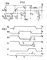
- the memory cell of a dynamic semiconductor random access memory is denoted by Z. It contains a p-channel selection transistor T1 and a storage capacitor C1. Both are connected to each other in series and are located between the connection 1 of a bit line BL and a connection 2, which is connected to a reference potential.
- a word line 3, which is connected to the gate of T1, is used to address the memory cell Z. In the unselected state of the word line 3, this is at a voltage level, which corresponds to the supply voltage V DD , while in the selected state, in which the storage capacitor C1 is connected to the bit line BL via the conductive selection transistor T1, is set to a low potential.
- the potential control of the word line 3 takes place via the output 4 of a decoder D, which has a p-channel transistor T2 in a first switching branch 5 and an n-channel transistor T31 to T3n in n second switching branches 61 to 6n.
- the switching branch 5 is between a terminal 6, which is connected to the supply voltage V DD , and the output 4, while the switching branches 61 to 6n are each between 4 and the reference potential of the circuit.
- the output 4 of the decoder D is connected to the gate of an n-channel transistor T5, via which the word line 3 is led to a terminal 7.
- a p-channel transistor T6, the gate of which is at reference potential, is inserted into the connection of the output 4 to the gate of T5.
- the gate of T5 is connected to terminal 7 via a capacitance C.
- a p-channel transistor T8, which is connected between the terminal 6 and the word line 3, is provided with a gate terminal 8.
- the line capacitance of the word line 3 is finally indicated by a capacitance C WL , the connecting lines of which are shown in broken lines.
- word line 3 is supplied with supply voltage V OD via conductive transistor T8.
- a voltage WA8 (FIG. 2) is supplied to the gate terminal 8, which is 0 volts.
- the voltage PRE present at the gate terminal 10 of T2 is now raised from 0 volts to V DD , as a result of which the output 4, which had charged up to V DD prior to tl when the transistor T2 was conducting, Block T2 from VDO is switched off. 4 is then in the "floating" state as long as PRE is on V DD .
- n address signals A O to A (n-1) are fed to the correspondingly designated gate connections from T31 to T3n, which is indicated in FIG. 2 by the voltage profile A i . If all address signals have a value of 0 volts, which is indicated in FIG. 2 by the course of A i denoted by 11, then all transistors T 31 to T3n remain blocked (selection of word line 3). This means that output 4 does not discharge significantly during the addressing process.
- the word line 3 is driven in such a way that it is discharged to a low potential during the entire addressing process, as will be explained in detail below.
- the selection transistors, for example T1 of the adjacent 3 memory cells, for example Z become conductive and switch the storage capacitors, for example Cl, to the associated bit lines BL (addressing of the memory cells).
- the potential control of the word line 3 as a function of the potential that arises at the output 4 of the decoder 0 after the time t2 proceeds in detail as follows:
- the increase from WA8 to V DD beginning at the time t3 blocks the transistor T8, whereby the word line 3 from the terminal 6 is shuttered is tet and in the state of "floating".
- a drive voltage WA7 is supplied to terminal 7, which alternates between an upper value VOD and a lower value of, for example, -2 volts.
- WA7 has the upper value V DD before t3, while a drop to -2 volts occurs after t3.
- T5 becomes conductive when WA7 drops to -2 volts, since its gate remains controlled with V DD .
- the word line 3 now receives a defined voltage of -2 volts via T5 and 7, so that C WL is charged from V DD to -2 volts, as the curve WL of the voltage on the word line 3 shows.
- the selection transistor is driven into the conductive state to the extent that it maintains the conductive connection between Cl and the bit line BL, which is at 0 volts, not only when the node 13 is at a potential which corresponds to V DD , but also when 13 has discharged to 0 volts.
- the transistor T6 is conductive because of the voltage V DD at the output 4 and its gate which is at reference potential.
- the addressing process is ended at time t4.
- the drive voltage WA7 is again raised to V DD , so that T5 blocks, while WA8 is lowered to 0 volts, so that the voltage WL on word line 3 rises to V DD via conductive transistor T8 (FIG. 2).
- T5 remains after the point in time during the sinking of WA7 t3 locked. Even if WA7 reaches the lower voltage value of -2 volts, a corresponding voltage drop is transmitted to the gate of T5 via the capacitance C, so that it then also reliably blocks. Transistor T6 blocks when this voltage drop occurs so that the gate of T5 is not raised to 0 volts via conductive transistors T31 through T3n (which could cause T5 to conduct again).
- the voltage WL on the word line 3 remains in the “floating” state during the entire addressing process, specifically at a voltage level of V DD , which is indicated in FIG. 2 by the dashed curve 14 of WL.
- the addressing process is ended again, which happens due to an increase in the drive voltage WA7 to VDD and a drop in the voltage WA8 to 0 volts.
- the word line 3 is thus connected to the supply voltage V DD via the conductive transistor T8, while nothing changes in the blocked state of T5.
- a preferred development of the invention consists in that the word line 3 is connected to the terminal 6 via a p-channel transistor T4, the gate of T4 being connected to the output 4 of the decoder D.
- the connecting lines of T4 are shown in broken lines in FIG. 1. With T4 it is achieved that the word line 3 in the unselected state, in which the output 4 is reduced to 0 volts, is connected to the supply voltage VOD via the then conductive transistor T4, so that the above-described state of the "floating" of the word line is replaced by the connection to a defined potential .
- the advantage is that the coupling of interference voltages cannot lead to an undesired selection of the word line 3.
- a p-channel transistor T7 is connected between the terminal 6 and the output 4 of the decoder D, the gate of which is connected to the word line 3.
- T7 conducts in the selected state of the word line, the potential of which is lowered to -2 volts, and switches V DD to output 4 and thus to the gate of T5. This prevents the output 4 from being discharged by possible leakage currents during a long selection of the word line 3.
- T9 In the circuit according to the invention, it can also be expedient to connect the output 4 of the decoder D to the reference potential via an n-channel transistor T9.
- the gate terminal 9 of T9 is assigned a voltage V9, which is shown in Fig. 2. If V9 is raised from 0 volts to a value V DD before the start of the rising edge of WA7, ie before t4, T9 conducts and prevents a voltage increase corresponding to this edge at output 4 or at the gate of T5 above the value of V DD out. Such an increase in voltage could lead to the formation of undesired current paths in the circuit and thus to a thermal overload of the same.
- the transistors of the one channel type used are each replaced by those of the other channel type, and instead of the voltages or voltage values previously mentioned, those of the opposite sign are used.
- the memory cells Z described so far, including the p-channel selection transistors T1 are each located in individually assigned n-type trough-shaped subregions of a p-type semiconductor body on which the memory is built, the memory cells modified according to this are with n- Channel selection transistors equipped and provided in p-type trough-shaped sub-areas of an n-type semiconductor body.
Landscapes
- Engineering & Computer Science (AREA)
- Microelectronics & Electronic Packaging (AREA)
- Computer Hardware Design (AREA)
- Dram (AREA)
- Semiconductor Memories (AREA)
Abstract
Description
- Die Erfindung bezieht sich auf eine integrierte Schaltung für einen in komplementärer Schaltungstechnik aufgebauten dynamischen Halbleiterspeicher mit wahlfreiem Zugriff nach dem Oberbegriff des Patentanspruchs 1.
- Eine solche Schaltung ist beispielsweise aus den IEEE Transactions on Electron Devices, Vol. ED-29, No. 4, April 1982, Seiten 714-718, insbesondere Fig. 2, bekannt. Hierbei handelt es sich um p-Kanal-Auswahltransistoren und n-Kanal-Schalttransistoren, über die die Wortleitungen jeweils vom nichtselektierten Zustand in den selektierten Zustand geschaltet werden. Die hierzu erforderliche Umladung der Wortleitungskapazitäten erfolgt zwar schneller, als dies bei n-Kanal-Auswahltransistoren der Fall wäre, doch kann der Speicherkondensator einer adressierten Speicherzelle über einen p-Kanal-Auswahltransistor und einen n-Kanal-Schalttransistor nur auf ein Potential entladen werden, das der Einsatzspannung des Auswahltransistors entspricht. Ein weiteres Absinken der Spannung am Speicherkondensator wird durch das Sperren des Auswahltransistors verhindert. Somit steht nicht der volle durch die Versorgungsspannung und das Bezugspotential gegebene Spannungshub für die Speicherung digitaler Signale zur Verfügung.
- Der Erfindung liegt die Aufgabe zugrunde, eine integrierte Schaltung der eingangs genannten Art anzugeben, St 1 Sti/9.7.1984 bei der dieser Nachteil nicht auftritt. Das wird erfindungsgemäß durch eine Ausbildung der Schaltung nach dem kennzeichnenden Teil des Patentanspruchs 1 erreicht.
- Der mit der Erfindung erzielbare Vorteil besteht insbesondere darin, daß auf der Wortleitung eine so große Potentialdifferenz zwischen den beiden im selektierten und im nichtselektierten Zustand herrschenden Potentialzuständen erreicht wird, daß der den Speicherzellen über die Bitleitungen zuführbare volle Spannungshub, der durch die Versorgungsspannung und das Bezugspotential gegeben ist, für die Speicherung von digitalen Signalen zur Verfügung steht.
- Die Ansprüche 2 bis 5 sind auf bevorzugte Ausgestaltungen und Weiterbildungen der Erfindung gerichtet.
- Die Erfindung wird nachfolgend anhand der Zeichnung näher beschrieben. Dabei zeigt:
- Fig. 1 ein bevorzugtes Ausführungsbeispiel der Erfindung und
- Fig. 2 Spannungs-Zeitdiagramme zur Erläuterung von Fig. 1.
- In Fig. 1 ist die Speicherzelle eines dynamischen Halbleiterspeichers mit wahlfreiem Zugriff (DRAM) mit Z bezeichnet. Sie enthält einen p-Kanal-Auswahltransistor Tl und einen Speicherkondensator Cl. Beide sind zueinander in Serie geschaltet und liegen zwischen dem Anschluß 1 einer Bitleitung BL und einem Anschluß 2, der mit einem Bezugspotential beschaltet ist. Zur Adressierung der Speicherzelle Z dient eine Wortleitung 3, die mit dem Gate von Tl verbunden ist. Im nichtselektierten Zustand der Wortleitung 3 liegt diese auf einem Spannungspegel, der der Versorgungsspannung VDD entspricht, während sie im selektierten Zustand, in dem der Speicherkondensator Cl über den leitenden Auswahltransistor Tl an die Bitleitung BL angeschaltet ist, auf ein niedriges Potential gelegt wird. Die potentialmäßige Ansteuerung der Wortleitung 3 erfolgt über den Ausgang 4 eines Dekoders D, der in einem ersten Schaltzweig 5 einen p-Kanal-Transistor T2 und in n zweiten Schaltzweigen 61 bis 6n jeweils einen n-Kanal-Transistor T31 bis T3n aufweist. Der Schaltzweig 5 liegt zwischen einem Anschluß 6, der mit der Versorgungsspannung VDD beschaltet ist, und dem Ausgang 4, während die Schaltzweige 61 bis 6n jeweils zwischen 4 und dem Bezugspotential der Schaltung liegen.
- Der Ausgang 4 des Dekoders D ist mit dem Gate eines n-Kanal-Transistors T5 verbunden, über den die Wortleitung 3 an einen Anschluß 7 geführt ist. In die Verbindung des Ausgangs 4 mit dem Gate von T5 ist ein p-Kanal-Transistor T6 eingefügt, dessen Gate auf Bezugspotential liegt. Das Gate von T5 ist über eine Kapazität C mit dem Anschluß 7 verbunden. Ein p-Kanal-Transistor T8, der zwischen den Anschluß 6 und die Wortleitung 3 geschaltet ist, ist mit einem Gateanschluß 8 versehen. Die Leitungskapazität der Wortleitung 3 ist schließlich durch eine Kapazität CWL angedeutet, deren Anschlußleitungen gestrichelt dargestellt sind.
- Vor einem Adressiervorgang ist die Wortleitung 3 über den leitenden Transistor T8 mit der Versorgungsspannung VOD belegt. Hierzu wird dem Gateanschluß 8 eine Spannung WA8 (Fig. 2) zugeführt, die 0 Volt beträgt. Zu Beginn des Adressiervorgangs, d.h. zum Zeitpunkt tl, wird nun die am Gateanschluß 10 von T2 anliegende Spannung PRE von 0 Volt auf VDD angehoben, wodurch der Ausgang 4, der sich vor tl bei leitendem Transistor T2 auf VDD aufgeladen hatte, durch das Sperren von T2 von VDO abgeschaltet wird. 4 befindet sich dann im Zustand des "floating", solange PRE auf VDD liegt. Zum Zeitpunkt t2 werden n Adressensignale AO bis A(n-1) den entsprechend bezeichneten Gateanschlüssen von T31 bis T3n zugeführt, was in Fig. 2 durch den Spannungsverlauf Ai angedeutet ist. Haben sämtliche Adressensignale einen Wert von 0 Volt, was in Fig. 2 durch den mit 11 bezeichneten Verlauf von Ai angedeutet ist, so bleiben alle Transistoren T 31 bis T3n gesperrt (Selektion der Wortleitung 3). Das bedeutet, daß sich der Ausgang 4 während des Adressiervorgangs nicht wesentlich entlädt. Dabei wird die Wortleitung 3 so angesteuert, daß sie während des ganzen Adressiervorgangs auf ein niedriges Potential entladen wird, wie weiter unten im einzelnen erläutert wird. Die Auswahltransistoren, z.B. Tl, der an.3 liegenden Speicherzellen , z.B. Z, werden leitend und schalten die Speicherkondensatoren, z.B. Cl, an die zugehörigen Bitleitungen BL (Adressierung der Speicherzellen).
- Wenn andererseits wenigstens eines der Adressensignale A0 bis A(n-1) einen Wert von VDD annimmt, was durch den gestrichelt gezeichneten Verlauf 12 von Ai ausgedrückt, wird, entlädt sich der Ausgang 4 auf 0 Volt, was dazu führt, daß die Wortleitung 3 während des ganzen Adres- .siervorgangs etwa auf VDD gehalten wird. Das entspricht dem nichtselektierten Zustand der Wortleitung 3, wobei die an ihr liegenden Speicherzellen, z.B. Z, nicht adressiert sind.
- Die potentialmäßige Ansteuerung der Wortleitung 3 in Abhängigkeit von dem Potential, das sich am Ausgang 4 des Dekoders 0 nach dem Zeitpunkt t2 einstellt, geht im einzelnen wie folgt vor sich: Der zum Zeitpunkt t3 beginnende Anstieg von WA8 auf VDD sperrt den Transistor T8, wodurch die Wortleitung 3 vom Anschluß 6 abgeschaltet wird und in den Zustand des "floating" gelangt. Dem Anschluß 7 wird eine Ansteuerspannung WA7 zugeführt, die zwischen einem oberen Wert VOD und einem unteren Wert von z.B. -2 Volt alterniert. Vor t3 weist WA7 den oberen Wert VDD auf, während nach t3 ein Abfall auf -2 Volt eintritt. Setzt man voraus, daß der Ausgang 4 während des Adressiervorgangs auf dem VDD entsprechenden Potential verbleibt (Selektion von 3), so wird T5 beim Abfall von WA7 auf -2 Volt leitend, da sein Gate mit VDD angesteuert bleibt. Die Wortleitung 3 erhält jetzt über T5 und 7 eine definierte Spannung von -2 Volt zugeführt, so daß CWL von VDD auf -2 Volt umgeladen wird, wie der Verlauf WL der Spannung auf der Wortleitung 3 zeigt. Als Folge davon wird der Auswahltransistor soweit in den leitenden Zustand ausgesteuert, daß er die leitende Verbindung zwischen Cl und der auf 0 Volt liegenden Bitleitung BL nicht nur dann aufrechterhält, wenn sich der Knoten 13 auf einem Potential befindet, das VDD entspricht, sondern auch dann, wenn sich 13 auf 0 Volt entladen hat.
- Auf diese Weise gelingt es, die vorher auf VDD aufgeladene Speicherkapazität Cl auf 0 Volt umzuladen, wenn die auf 0 Volt liegende Bitleitung BL über Tl an den Knoten 13 angeschaltet wird. Bei herkömmlichen SchalL tungen dieser Art, bei denen die Wortleitung 3 im selektierten Zustand nur auf 0 Volt abgesenkt wird, bleibt bei einer entsprechenden Umladung von Cl am Knoten 13 eine Restspannung bestehen, die dem Wert der Einsatzspannung von Tl, also z.B. 1,5 Volt, entspricht.
- Im betrachteten selektierten Zustand der Wortleitung 3 ist der Transistor T6 wegen der Spannung VDD am Ausgang 4 und seinem auf Bezugspotential liegenden Gate leitend. Zum Zeitpunkt t4 wird der Adressiervorgang beendet. Hierzu wird die Ansteuerspannung WA7 wieder auf VDD angehoben, so daß T5 sperrt, während WA8 auf 0 Volt abgesenkt wird, so daß die Spannung WL auf der Wortleitung 3 über den leitenden Transistor T8 auf VDD ansteigt (Fig. 2).
- Wenn sich der Ausgang 4 des Dekoders D bei einer Nicht-Selektion der Wortleitung 3 (Verlauf 12 von Ai) nach t2 über wenigstens einen leitend geschaltenen Transistor T31 bis T3n auf 0 Volt entlädt, bleibt T5 während des Absinkens von WA7 nach dem Zeitpunkt t3 gesperrt. Auch wenn WA7 den unteren Spannungswert von -2 Volt erreicht, wird über die Kapazität C eine entsprechende Spannungsabsenkung auf das Gate von T5 übertragen, so daß dieser auch dann sicher sperrt. Der Transistor T6 sperrt beim Auftreten dieser Spannungsabsenkung, so daß das Gate von T5 nicht etwa über den oder die leitenden Transistoren T31 bis T3n auf 0 Volt angehoben wird (was dazu führen könnte, daß T5 wieder leitet). Die Spannung WL auf der Wortleitung 3 bleibt in diesem Fall während des ganzen Adressiervorgangs in dem bereits beschriebenen Zustand des "floating", und zwar auf einem Spannungspegel von VDD, was in Fig. 2 durch den gestrichelten Verlauf 14 von WL angedeutet ist. Zum Zeitpunkt t4 wird der Adressiervorgang wieder beendet, was durch einen Anstieg der Ansteuerspannung WA7 auf VDD und einen Abfall der Spannung WA8 auf 0 Volt geschieht. Damit wird die Wortleitung 3 über den leitenden Transistor T8 mit der Versorgungsspannung VDD beschaltet, während sich am gesperrten Zustand von T5 nichts ändert.
- Eine bevorzugte Weiterbildung der Erfindung besteht darin, daß die Wortleitung 3 über einen p-Kanal-Transistor T4 mit dem Anschluß 6 verbunden ist, wobei das Gate von T4 an den Ausgang 4 des Dekoders D geschaltet ist. Die Anschlußleitungen von T4 sind in Fig. 1 gestrichelt eingezeichnet. Mit T4 wird erreicht, daß die Wortleitung 3 im nichtselektierten Zustand, in dem der Ausgang 4 auf 0 Volt abgesenkt wird, über den dann leitenden Transistor T4 mit der Versorgungsspannung VOD beschaltet ist, so daß der oben beschriebene Zustand des "floating" der Wortleitung durch die Anschaltung an ein definiertes Potential ersetzt ist. Der Vorteil besteht darin, daß Einkopplungen von Störspannungen nicht zu einer unerwünschten Selektion der Wortleitung 3 führen können.
- Nach einer anderen Weiterbildung der Erfindung ist ein p-Kanal-Transistor T7 zwischen den Anschluß 6 und den Ausgang 4 des Dekoders D geschaltet, dessen Gate mit der Wortleitung 3 verbunden ist. T7 leitet im selektierten Zustand der Wortleitung, deren Potential dabei auf -2 Volt abgesenkt ist, und schaltet VDD auf den Ausgang 4 und damit auf das Gate von T5. Damit wird verhindert, daß sich der Ausgang 4 bei einer lange andauernden Selektion der Wortleitung 3 durch eventuelle Leckströme entlädt.
- Bei der erfindungsgemäßen Schaltung kann es auch zweckmäßig sein, den Ausgang 4 des Dekoders D über einen n-Kanal-Transistor T9 mit dem Bezugspotential zu beschalten. Der Gateanschluß 9 von T9 ist dabei mit einer Spannung V9 belegt, die in Fig. 2 dargestellt ist. Wird V9 vor dem Beginn der ansteigenden Flanke von WA7, d.h. vor t4, von 0 Volt auf einen Wert VDD angehoben, so leitet T9 und verhindert eine dieser Flanke entsprechende Spannungserhöhung am Ausgang 4 bzw. am Gate von T5 über den Wert von VDD hinaus. Eine solche Spannungserhöhung könnte zur Ausbildung von unerwünschten Strompfaden in der Schaltung und damit zu einer thermischen Überlastung derselben führen.
- Neben den oben beschriebenen Ausführungsformen der Erfindung sind auch solche von Interesse, bei denen die isher verwendeten Transistoren des einen Kanaltyps jeweils durch solche des anderen Kanaltyps ersetzt sind, wobei anstelle der bisher genannten Spannungen bzw. Spannungswerte solche des jeweils entgegengesetzten Vorzeichens verwendet werden. Während sich die bisher beschriebenen Speicherzellen Z einschließlich der p-Kanal-Auswahltransistoren Tl jeweils in individuell zugeordneten n-leitenden wannenförmigen Teilgebieten eines p-leitenden Halbleiterkörpers befinden, auf dem der Speicher aufgebaut ist, sind die hiernach ab- gewandel.ten Speicherzellen mit n-Kanal-Auswahltransistoren ausgestattet und in p-leitenden wannenförmigen Teilgebieten eines n-leitenden Halbleiterkörpers vorgesehen.
Claims (5)
Priority Applications (1)
| Application Number | Priority Date | Filing Date | Title |
|---|---|---|---|
| AT85108682T ATE64229T1 (de) | 1984-07-25 | 1985-07-11 | Integrierte schaltung eines in komplementaerer schaltungstechnik aufgebauten dynamischen halbleiterspeichers. |
Applications Claiming Priority (2)
| Application Number | Priority Date | Filing Date | Title |
|---|---|---|---|
| DE3427454 | 1984-07-25 | ||
| DE19843427454 DE3427454A1 (de) | 1984-07-25 | 1984-07-25 | Integrierte schaltung fuer einen in komplementaerer schaltungstechnik aufgebauten dynamischen halbleiterspeicher |
Publications (3)
| Publication Number | Publication Date |
|---|---|
| EP0169452A2 true EP0169452A2 (de) | 1986-01-29 |
| EP0169452A3 EP0169452A3 (en) | 1988-01-13 |
| EP0169452B1 EP0169452B1 (de) | 1991-06-05 |
Family
ID=6241554
Family Applications (1)
| Application Number | Title | Priority Date | Filing Date |
|---|---|---|---|
| EP85108682A Expired - Lifetime EP0169452B1 (de) | 1984-07-25 | 1985-07-11 | Integrierte Schaltung eines in komplementärer Schaltungstechnik aufgebauten dynamischen Halbleiterspeichers |
Country Status (6)
| Country | Link |
|---|---|
| US (1) | US4763301A (de) |
| EP (1) | EP0169452B1 (de) |
| JP (1) | JPS6139993A (de) |
| AT (1) | ATE64229T1 (de) |
| DE (2) | DE3427454A1 (de) |
| HK (1) | HK28393A (de) |
Cited By (2)
| Publication number | Priority date | Publication date | Assignee | Title |
|---|---|---|---|---|
| EP0212946A3 (en) * | 1985-08-14 | 1988-08-31 | Fujitsu Limited | Semiconductor memory device |
| US5051959A (en) * | 1985-08-14 | 1991-09-24 | Fujitsu Limited | Complementary semiconductor memory device including cell access transistor and word line driving transistor having channels of different conductivity type |
Families Citing this family (1)
| Publication number | Priority date | Publication date | Assignee | Title |
|---|---|---|---|---|
| US5185721A (en) * | 1988-10-31 | 1993-02-09 | Texas Instruments Incorporated | Charge-retaining signal boosting circuit and method |
Family Cites Families (8)
| Publication number | Priority date | Publication date | Assignee | Title |
|---|---|---|---|---|
| DE2443490A1 (de) * | 1974-09-11 | 1976-03-25 | Siemens Ag | Schalter aus mos-transistoren |
| JPS51130154A (en) * | 1975-05-07 | 1976-11-12 | Nec Corp | Flip-flop circuit |
| DE2641693C2 (de) * | 1976-09-16 | 1978-11-16 | Siemens Ag, 1000 Berlin Und 8000 Muenchen | Decodierschaltung mit MOS-Transistoren |
| JPS5493335A (en) * | 1977-12-30 | 1979-07-24 | Fujitsu Ltd | Decoder circuit |
| JPS5647988A (en) * | 1979-09-20 | 1981-04-30 | Nec Corp | Semiconductor memory device |
| JPS57196627A (en) * | 1981-05-29 | 1982-12-02 | Hitachi Ltd | Electronic circuit device |
| JPS5954096A (ja) * | 1982-09-22 | 1984-03-28 | Hitachi Ltd | ダイナミツク型mosram |
| US4618784A (en) * | 1985-01-28 | 1986-10-21 | International Business Machines Corporation | High-performance, high-density CMOS decoder/driver circuit |
-
1984
- 1984-07-25 DE DE19843427454 patent/DE3427454A1/de not_active Withdrawn
-
1985
- 1985-07-01 US US06/750,145 patent/US4763301A/en not_active Expired - Lifetime
- 1985-07-11 DE DE8585108682T patent/DE3583075D1/de not_active Expired - Lifetime
- 1985-07-11 AT AT85108682T patent/ATE64229T1/de not_active IP Right Cessation
- 1985-07-11 EP EP85108682A patent/EP0169452B1/de not_active Expired - Lifetime
- 1985-07-19 JP JP15999485A patent/JPS6139993A/ja active Granted
-
1993
- 1993-03-25 HK HK283/93A patent/HK28393A/xx not_active IP Right Cessation
Cited By (2)
| Publication number | Priority date | Publication date | Assignee | Title |
|---|---|---|---|---|
| EP0212946A3 (en) * | 1985-08-14 | 1988-08-31 | Fujitsu Limited | Semiconductor memory device |
| US5051959A (en) * | 1985-08-14 | 1991-09-24 | Fujitsu Limited | Complementary semiconductor memory device including cell access transistor and word line driving transistor having channels of different conductivity type |
Also Published As
| Publication number | Publication date |
|---|---|
| JPS6139993A (ja) | 1986-02-26 |
| ATE64229T1 (de) | 1991-06-15 |
| US4763301A (en) | 1988-08-09 |
| DE3583075D1 (de) | 1991-07-11 |
| EP0169452B1 (de) | 1991-06-05 |
| JPH0585992B2 (de) | 1993-12-09 |
| EP0169452A3 (en) | 1988-01-13 |
| HK28393A (en) | 1993-04-02 |
| DE3427454A1 (de) | 1986-01-30 |
Similar Documents
| Publication | Publication Date | Title |
|---|---|---|
| DE69027705T2 (de) | Spannungserhöhungsschaltung für dynamische Speicher | |
| DE2324965B2 (de) | Schaltungsanordnung zum Auslesen eines kapazitiven Datenspeichers | |
| DE2525225A1 (de) | Schaltungsanordnung zur anzeige der verschiebung elektrischer ladung | |
| DE69126292T2 (de) | PMOS-Wortleitung Speisespannungsverstärkungsschaltung für DRAM | |
| DE3531580A1 (de) | Speicheranordnung | |
| DE2430690A1 (de) | Integrierter halbleiterspeicher | |
| DE2721851A1 (de) | Verriegelnder leseverstaerker fuer halbleiterspeicheranordnungen | |
| DE4336907A1 (de) | Substratpotential-Erzeugungsschaltung zum Erzeugen eines Substratpotentials mit einem niedrigen Pegel und Halbleitervorrichtung mit einer solchen Schaltung | |
| DE2413804C2 (de) | Schaltungsanordnung für eine wortorganisierte Halbleiterspeichermatrix | |
| DE4226844A1 (de) | Datenuebertragungsschaltkreis | |
| DE4117882C2 (de) | ||
| DE3329096C2 (de) | ||
| DE2845100A1 (de) | Speicherschaltung | |
| DE3307756C2 (de) | ||
| DE2754987A1 (de) | Leistungslose halbleiter-speichervorrichtung | |
| DE3430144A1 (de) | Halbleiter-speichereinrichtung | |
| EP0169452B1 (de) | Integrierte Schaltung eines in komplementärer Schaltungstechnik aufgebauten dynamischen Halbleiterspeichers | |
| DE4237001C2 (de) | Integrierte Halbleiterschaltungsvorrichtung | |
| DE2702830C2 (de) | ||
| EP0297276B1 (de) | Generatorschaltung | |
| DE2131939B2 (de) | Logisch gesteuerte Inverterstufe | |
| DE10322544B3 (de) | DRAM-Speicherschaltung | |
| EP0045399B1 (de) | Monolithisch integrierter Halbleiterspeicher | |
| DE2103276A1 (de) | Dynamisches Schieberegister | |
| DE2636377C3 (de) | Binärspeicherzelle |
Legal Events
| Date | Code | Title | Description |
|---|---|---|---|
| PUAI | Public reference made under article 153(3) epc to a published international application that has entered the european phase |
Free format text: ORIGINAL CODE: 0009012 |
|
| AK | Designated contracting states |
Designated state(s): AT DE FR GB IT NL |
|
| PUAL | Search report despatched |
Free format text: ORIGINAL CODE: 0009013 |
|
| AK | Designated contracting states |
Kind code of ref document: A3 Designated state(s): AT DE FR GB IT NL |
|
| 17P | Request for examination filed |
Effective date: 19880712 |
|
| 17Q | First examination report despatched |
Effective date: 19891127 |
|
| GRAA | (expected) grant |
Free format text: ORIGINAL CODE: 0009210 |
|
| AK | Designated contracting states |
Kind code of ref document: B1 Designated state(s): AT DE FR GB IT NL |
|
| REF | Corresponds to: |
Ref document number: 64229 Country of ref document: AT Date of ref document: 19910615 Kind code of ref document: T |
|
| REF | Corresponds to: |
Ref document number: 3583075 Country of ref document: DE Date of ref document: 19910711 |
|
| ET | Fr: translation filed | ||
| ITF | It: translation for a ep patent filed | ||
| GBT | Gb: translation of ep patent filed (gb section 77(6)(a)/1977) | ||
| PLBE | No opposition filed within time limit |
Free format text: ORIGINAL CODE: 0009261 |
|
| STAA | Information on the status of an ep patent application or granted ep patent |
Free format text: STATUS: NO OPPOSITION FILED WITHIN TIME LIMIT |
|
| 26N | No opposition filed | ||
| REG | Reference to a national code |
Ref country code: GB Ref legal event code: IF02 |
|
| PGFP | Annual fee paid to national office [announced via postgrant information from national office to epo] |
Ref country code: AT Payment date: 20020619 Year of fee payment: 18 |
|
| PG25 | Lapsed in a contracting state [announced via postgrant information from national office to epo] |
Ref country code: AT Free format text: LAPSE BECAUSE OF NON-PAYMENT OF DUE FEES Effective date: 20030711 |
|
| PGFP | Annual fee paid to national office [announced via postgrant information from national office to epo] |
Ref country code: NL Payment date: 20040630 Year of fee payment: 20 |
|
| PGFP | Annual fee paid to national office [announced via postgrant information from national office to epo] |
Ref country code: GB Payment date: 20040823 Year of fee payment: 20 |
|
| PGFP | Annual fee paid to national office [announced via postgrant information from national office to epo] |
Ref country code: FR Payment date: 20040910 Year of fee payment: 20 |
|
| PGFP | Annual fee paid to national office [announced via postgrant information from national office to epo] |
Ref country code: DE Payment date: 20040914 Year of fee payment: 20 |
|
| PG25 | Lapsed in a contracting state [announced via postgrant information from national office to epo] |
Ref country code: GB Free format text: LAPSE BECAUSE OF EXPIRATION OF PROTECTION Effective date: 20050710 |
|
| PG25 | Lapsed in a contracting state [announced via postgrant information from national office to epo] |
Ref country code: NL Free format text: LAPSE BECAUSE OF EXPIRATION OF PROTECTION Effective date: 20050711 |
|
| REG | Reference to a national code |
Ref country code: GB Ref legal event code: PE20 |
|
| NLV7 | Nl: ceased due to reaching the maximum lifetime of a patent |
Effective date: 20050711 |