EP0169519A2 - Halbleitervorrichtung und Verfahren zu ihrer Herstellung - Google Patents
Halbleitervorrichtung und Verfahren zu ihrer Herstellung Download PDFInfo
- Publication number
- EP0169519A2 EP0169519A2 EP85109095A EP85109095A EP0169519A2 EP 0169519 A2 EP0169519 A2 EP 0169519A2 EP 85109095 A EP85109095 A EP 85109095A EP 85109095 A EP85109095 A EP 85109095A EP 0169519 A2 EP0169519 A2 EP 0169519A2
- Authority
- EP
- European Patent Office
- Prior art keywords
- edge
- thin film
- semiconductor body
- openings
- depression
- Prior art date
- Legal status (The legal status is an assumption and is not a legal conclusion. Google has not performed a legal analysis and makes no representation as to the accuracy of the status listed.)
- Granted
Links
Images


Classifications
-
- H—ELECTRICITY
- H10—SEMICONDUCTOR DEVICES; ELECTRIC SOLID-STATE DEVICES NOT OTHERWISE PROVIDED FOR
- H10D—INORGANIC ELECTRIC SEMICONDUCTOR DEVICES
- H10D62/00—Semiconductor bodies, or regions thereof, of devices having potential barriers
- H10D62/40—Crystalline structures
- H10D62/405—Orientations of crystalline planes
-
- G—PHYSICS
- G01—MEASURING; TESTING
- G01F—MEASURING VOLUME, VOLUME FLOW, MASS FLOW OR LIQUID LEVEL; METERING BY VOLUME
- G01F1/00—Measuring the volume flow or mass flow of fluid or fluent solid material wherein the fluid passes through a meter in a continuous flow
- G01F1/68—Measuring the volume flow or mass flow of fluid or fluent solid material wherein the fluid passes through a meter in a continuous flow by using thermal effects
- G01F1/684—Structural arrangements; Mounting of elements, e.g. in relation to fluid flow
-
- G—PHYSICS
- G01—MEASURING; TESTING
- G01F—MEASURING VOLUME, VOLUME FLOW, MASS FLOW OR LIQUID LEVEL; METERING BY VOLUME
- G01F1/00—Measuring the volume flow or mass flow of fluid or fluent solid material wherein the fluid passes through a meter in a continuous flow
- G01F1/68—Measuring the volume flow or mass flow of fluid or fluent solid material wherein the fluid passes through a meter in a continuous flow by using thermal effects
- G01F1/684—Structural arrangements; Mounting of elements, e.g. in relation to fluid flow
- G01F1/6842—Structural arrangements; Mounting of elements, e.g. in relation to fluid flow with means for influencing the fluid flow
-
- G—PHYSICS
- G01—MEASURING; TESTING
- G01F—MEASURING VOLUME, VOLUME FLOW, MASS FLOW OR LIQUID LEVEL; METERING BY VOLUME
- G01F1/00—Measuring the volume flow or mass flow of fluid or fluent solid material wherein the fluid passes through a meter in a continuous flow
- G01F1/68—Measuring the volume flow or mass flow of fluid or fluent solid material wherein the fluid passes through a meter in a continuous flow by using thermal effects
- G01F1/684—Structural arrangements; Mounting of elements, e.g. in relation to fluid flow
- G01F1/6845—Micromachined devices
-
- G—PHYSICS
- G01—MEASURING; TESTING
- G01F—MEASURING VOLUME, VOLUME FLOW, MASS FLOW OR LIQUID LEVEL; METERING BY VOLUME
- G01F1/00—Measuring the volume flow or mass flow of fluid or fluent solid material wherein the fluid passes through a meter in a continuous flow
- G01F1/68—Measuring the volume flow or mass flow of fluid or fluent solid material wherein the fluid passes through a meter in a continuous flow by using thermal effects
- G01F1/696—Circuits therefor, e.g. constant-current flow meters
-
- G—PHYSICS
- G01—MEASURING; TESTING
- G01F—MEASURING VOLUME, VOLUME FLOW, MASS FLOW OR LIQUID LEVEL; METERING BY VOLUME
- G01F1/00—Measuring the volume flow or mass flow of fluid or fluent solid material wherein the fluid passes through a meter in a continuous flow
- G01F1/68—Measuring the volume flow or mass flow of fluid or fluent solid material wherein the fluid passes through a meter in a continuous flow by using thermal effects
- G01F1/696—Circuits therefor, e.g. constant-current flow meters
- G01F1/698—Feedback or rebalancing circuits, e.g. self heated constant temperature flowmeters
- G01F1/699—Feedback or rebalancing circuits, e.g. self heated constant temperature flowmeters by control of a separate heating or cooling element
-
- H—ELECTRICITY
- H10—SEMICONDUCTOR DEVICES; ELECTRIC SOLID-STATE DEVICES NOT OTHERWISE PROVIDED FOR
- H10P—GENERIC PROCESSES OR APPARATUS FOR THE MANUFACTURE OR TREATMENT OF DEVICES COVERED BY CLASS H10
- H10P50/00—Etching of wafers, substrates or parts of devices
- H10P50/60—Wet etching
- H10P50/64—Wet etching of semiconductor materials
- H10P50/642—Chemical etching
- H10P50/644—Anisotropic liquid etching
Definitions
- the present invention relates to integrated semiconductor device technology in the field of sensors and radiant sources of electromagnetic energy. More specifically, the present invention relates to a method of fabrication and to structures of semiconductor devices of the class as described in prior EP-A 134 859, published 27.3.'985. Such devices have applications in areas including flow sensing, detection of combustible gases, humidity sensing, and pressure sensing. However, neither these devices nor the present invention is limited to such applications.
- the present invention comprises a method of fabricating a semiconductor device comprising a thin film member having a predetermined configuration bridging a depression etched into a first surface of a semiconductor body.
- the member is connected to the first surface at first and second substantially opposing ends of the predetermined configuration.
- the depression opens to the first surface along an edge on each side of the member.
- the method comprises the steps of providing a semiconductor body with a first surface having a predetermined orientation with respect to a crystalline structure in the semiconductor body.
- a layer of thin film material of which the member is comprised is applied onto the first surface.
- First and second openings are exposed through the thin film material to the first surface.
- the first opening is bounded in part by one edge of the member.
- the second opening is bounded in part by the other edge of the member.
- Both openings are also bounded in part by a boundary connected to an edge of the member. At least one of the boundaries has a predetermined boundary configuration formed so that, when an anisotropic etch is placed on the openings to undercut the member and form the depression, there will be no substantial undercutting of the semiconductor body below the thin film material at the predetermined boundary configuration.
- the present invention further comprises an integrated semiconductor device comprising a semiconductor body with a first surface having a predetermined orientation with respect to a crystalline structure in the semiconductor body.
- the semiconductor body has a depression formed into the first surface of the body.
- a layer of thin film material covers at least a portion of the first surface.
- a thin film member comprising the layer of material has a predetermined configuration bridging the depression.
- the member is connected to the first surface at substantially opposing ends of the predetermined configuration.
- the depression opens to the first surface along an edge on each side of the member.
- the layer of thin film material comprises first and second openings, the first opening being bounded in part by one edge of the member, the second opening being bounded in part by the other edge of the member.
- Both openings are also bounded in part by e boundary connected to an edge of the member. At least one of the boundaries has a predetermined boundary configuration formed so that, when an anisotropic etch is placed on the openings to undercut the member and form the depression, there will be no substantial undercutting of the semiconductor body below the thin film material at the predetermined boundary configuration.
- Substantially eliminating undercutting of the semiconductor body below the thin film material at the predetermined boundary configuration substantially eliminates overhang of the thin film material at these locations. Substantially avoiding such overhang is frequently important since such overhang is frequently wasted space on a semiconductor chip. Such area is unavailable for diodes on other electronic structures in the semiconductor body. Further, because of breakage possibilities in handling and processing, thin film conductors such as gold conductors on the order of 0.3-0.5 microns thick cannot be wisely placed there because they add stress to the overhang, which, if it fractures, will cause an open circuit as well as possible mechanical and thermal interference if a fragment is lodged, for example, under the bridged structures of the present invention. In addition, making the openings without substantial overhang facilitates air flow and/or thermal isolation of the bridged member from the semiconductor body.
- devices in accordance with the present invention avoid wasted space on semiconductor chips, enhance thermal isolation of elements on the bridged member, and result in small, less costly and more reliable chips and devices.
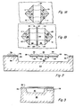
- Devices in accordance with the present invention can have a single bridged member such as illustrated in Figure lA or a plurality of bridged members such as 32 and 34 illustrated in Figure 1B and in Figures 1-5.
- Structures in accordance with the present invention typically comprise static electric, thermal-to-electric, and/or electric-to-thermal elements, usually in thin film form, as part of the bridged members. Such structures have many applications, including those listed above.
- the present invention comprises a method of fabricating a semiconductor device comprising a thin film member such as 32 or 34 having a predetermined configuration bridging a depression such as 30 etched into a first surface 36 of a semiconductor body 20.
- a member such as 32 or 34 is connected to first surface 36 at first and second substantially opposing ends of the predetermined configuration.
- Depression 30 opens to first surface 36 along an edge on each side of the member, e.g., edges such as 110 or 110A (member 34) or such as 110B or 110C (member 32).
- the method comprises the steps of providing a semiconductor body such as 20 with a first surface 36 having a predetermined orientation with respect to a crystalline structure in the semiconductor body.
- a layer such as 28 or 29 cf thin film material of which a member is comprised is applied to first surface 36.
- First and second openings such as 82 are exposed through the thin film material to first surface 36.
- the first opening is bounded in part by one edge of a member (e.g., edge 110) the second opening being bounded in part by the other edge of the member (e.g., edge 110A). Both openings are also bounded in part by a boundary connected to an edge of the member.
- At least one of the boundaries has a predetermined boundary configuration formed so that, when an anisotropic etch is placed on openings such as 82 to undercut members such as 32 or 34 and form a depression such as 30, there will be no substantial undercutting of the semiconductor body below the thin film material at the predetermined boundary configuration.
- Such a method results in a structure without substantial overhang of thin film materials such as 28 or 29 at the predetermined boundary configuration, and this is of advantage in many situations as previously indicated.
- a preferred method of fabricating the present invention includes providing a semiconductor body comprising (100) silicon having a (100) plane, a [110] direction, and a first surface such as 36 substantially parallel to the (100) plane.
- a layer of thin film material such as layers 28 and 29 of which members such as 32 or 34 are comprised is applied to first surface 36.
- First and second openings such as 82 are exposed through the thin film material to first surface 36. Openings such as 82 are defined so that members such as 32 or 34 are oriented at a non-zero angle to the [110] direction.
- the first opening such as 82 is bounded in part by one edge of a member (e.g., edge 110 of member 34), and the second opening such as 82 is bounded in part by the other edge of the member (e.g., edge 110A of member 34).
- Both openings such as 82 are also bounded in part by a boundary connected to an edge of the member. At least one of the boundaries has boundary components such as 111 substantially in line with the [110] direction or boundary components such as 113 substantially normal to the [110] direction.
- the preferred embodiment of a flow sensor comprising the present invention includes a pair of thin film heat sensors 22 and 24, a thin film heater 26, and a base 20 supporting the sensors and heater out of contact with the base. Sensors 22 and 24 are disposed on opposite sides of heater 26.
- Body 20 is preferrably a semiconductor body and preferrably silicon, chosen because of its adaptability to precision etching techniques and ease of electronic chip producibility.
- the sensor preferrably includes two identical temperature sensing resistor grids 22 and 24 acting as the thin film heat sensors and further includes a centrally located heater resistor grid 26 acting as the thin film heater.
- Sensors 22 and 24 and heater 26 are preferrably fabricated of nickel-iron, herein sometimes referred to as permalloy, having a preferred composition of 80% nickel and 20% iron.
- the sensor and heater grids are encapsulated in a thin film of dielectric, typically comprising layers 28 and 29 and preferrably silicon nitride, to form thin film members.
- the sensor comprises two thin film members 32 and 34, member 32 comprising sensor 22 and member 34 comprising sensor 24, each member comprising one-half of heater 26.
- the disclosed sensor further comprises an accurately defined air space which results in an air space effectively surrounding elements 22, 24, and 26.
- the effectively surrounding air space is achieved by fabricating the structure on silicon surface 36, thin film elements 22, 24, and 26 preferrably being encapsulated in thin film silicon nitride film, and by subsequently etching an accurately defined air space into silicon body 20 beneath members 32 and 34.
- Heater resistor grid 26 operates at a preferred constant average temperature difference of 100-200 degrees centigrade elevated above the temperature of silicon chip 20 which temperature is not appreciably different from the ambient air stream temperature. The power required by heater resistor 26 to achieve 200 degrees centigrade above ambient temperature is very small, being on the order of 0.010 watt.
- sensor grids 22 and 24 are precisely symmetrically located with respect to heater grid 26 so that at zero airflow they have identical temperatures and have no differences between their resistances. Consequently, a small probe current, 0.1-1.0 milli-amperes preferred, through both sensor resistances 22 and 24 will develop no voltage difference at zero airflow velocity.
- upstream resistors sensor 22 With airflow present, upstream resistors sensor 22 will be cooled by the transportation of heat away from sensor 22 toward heater resistor grid 26, whereas downstream sensor 24 will be heated by a transportation of heat toward the sensor from heat resistor grid 26. Consequently, a resistance difference between sensor resistances 22 and 24 will be present with a corresponding difference in voltage drop which is a measure of the air flow.
- Typical unamplified voltage differences can be as high as 0.1 volt at a 7,62 m/sec flow velocity.
- sensors 22 and 24 are operated with constant current such that temperature field changes can be sensed under flow conditions as previously described. Other operating arrangements are also possible.
- ambient temperature is monitored by a reference resistor 38 which is heat sunk onto semiconductor body 20.
- Resistor 38 may be a permalloy grid formed substantially like grids 22, 24 and 26 and is typically encapsulated in dielectric layers 28 and 29 and mounted on surface 36.
- reference resistor 38 being attached by the encapsulating dielectric directly to surface 36 of semiconductor body 20, readily monitors the temperature of the semiconductor body, which stays within 0.5 degrees centigrade of ambient temperature even with resistor grid 26 elevated to 200 degrees centigrade above ambient. Accordingly, heat sunk reference resistor 38 may be used to monitor ambient air flow temperature by monitoring a temperature that is very close to that of semiconductor body 20, which in turn is very close to ambient temperature.
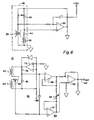
- heater 26 is operated at a constant temperature above ambient temperature, sensors 22 and 24 being operated at constant current, and the changing temperatures of sensors 22 and 24 are sensed as changes in resistance. Circuits for accomplishing these functions are illustrated in Figure 6. The smaller circuit controls the temperature of heater 26 while the larger circuit provides an output voltage that is proportional to the resistance difference between heat sensing resistors 22 and 24.
- the heater control circuit illustrated in Figure 6 uses a Wheatstone bridge 46 to maintain heater 26 at a constant temperature rise above ambient as sensed by heat sunk reference resistor 38.
- Wheatstone bridge 46 is shown comprising heater resistor 26 and a resistor 40 in its first leg and a resistor 42, heat sunk resistor 38 and a resistor 44 in its second leg.
- An error integrator comprising amplifier 50 keeps bridge 46 balanced by varying the potential across it and thus the power dissipated in heater 26.
- the circuity which monitors the resistance difference between downstream sensor 24 and upstream sensor 22 includes a constant current source 52 comprising an amplifier 72 and a differential amplifier 54 comprising amplifier 68 and 70.
- the constant current source drives a Wheatstone bridge comprising two high impedance resistors 56 and 58 in one leg and the two sensing resistors 22 and 24 with a nulling potentiometer 60 in the other leg.
- the gain of differential amplifier 54 is adjusted by potentiometer 62.
- Output 64 provides a voltage that is proportional tc the resistance difference between the two sensing resistors 22 and 24.
- Amplifiers 50, 66 and 72 may each comprise one-fourth of an LM324. Amplifiers 68 and 70 may each comprise one-half of an OP-10.
- upstream sensor resistor 22 preferrably has an inner edge 76 in close proximity (5 to 10 microns, for example) to the near edge 78 of heater resistor grid 26. At such a separation from near edge 78 of heater resistor grid 26, the zero flow air temperature near heater resistor edge 78 is close to that of edge 78. In a typical embodiment, where sensors 22 and 24 have a width of approximately 100 microns, outer edge 80 of sensor resistor grid 22 is located approximately 100 microns from near edge 78 of heater resistor grid 26. At the 100 micron separation, the zero airflow temperature is closer to that of the ambient air stream and to that of silicon chip 20 than it is to the temperature of heater resistor 26.
- outer edge 80 of sensor resistor grid 22 is easily cooled to near the limiting temperature of silicon chip 20 by low velocity airflow, whereas the inner regions of sensor resistor grid 22 (near edge 76) are more tightly coupled thermally to heater resistor 26 and respond more readily to the higher airflow velocity before the limiting temperature of the ambient airstream is approached. Accordingly, the composite effect of the temperature change from each resistor grid line (lines spaced over the approximately 5-100 micron distance from heater edge 76) for an increment of airflow is to keep the corresponding increment on the upstream resistor temperature response curve more nearly constant over a broad airflow range.
- areas 82 are cut in the silicon nitride to facilitate etching as further described below.
- Overall geometry, including that of leads 92, is preferably made symmetrically to insure symmetrical heat conduction properties on members 32 and 34 .
- Leads 92 connect to pad areas 90 for electrically connecting sensor elements 22, 24, 26, and 38 with circuitry 13 as previously discussed.
- Elements 22 and 24 have a preferred resistance in one example of 1200 ohms and element 26 has a preferred resistance in that example.of 520 ohms.
- sensors 22 and 24 have a width of approximately 100 microns and a length of approximately 175 microns.
- the proximal edges of sensors 22 and 24 are in close proximity(e.g., 5-10 microns) away from heater 26. That is, edge 76 of sensor 22 is 5-10 microns away from edge 78 of heater 26, and edge 84 of sensor 24 is 5-10 microns away from edge 86 of heater 26.
- the above dimensions are preferred dimensions which have been used in actual devices and are not deemed to be limiting, since these parameters could be substantially varied depending upon application.
- Sensing elements 22 and 24 may be located within the boundaries of a walled depression 30 as illustrated in Figure 2. Alternately, elements 22 and 2 4 may be located at the edge of a chip or body so that either the upstream portion of a depression 30A is open to receive flow unimpeded by a sidewall, as shown in Figure 4, or open at the downstream side so that flow may more easily exit, or be more easily drawn through, an air space 30AA as illustrated in Figure 5. Note that the embodiment of Figure 4 may be modified by removing at least a portion of the leading edge of body 20A, thus increasing the exposure of the leading edge of member 32A to flow; for example, portion 118 of body 20A may be removed back to line 120.
- the preferred process of fabricating the present sensor comprises providing a (100) silicon wafer 20 having a surface 36 which receives a layer 29 of silicon nitride.
- Layer 29 is typically 4000 angstroms thick and is typically deposited by standard sputtering techniques in a low pressure gas discharge.
- a uniform layer of permalloy typically 80% nickel and 20% iron and 800 angstroms thick, is deposited on the silicon nitride by sputtering.
- permalloy elements such as 22, 24, 26 and 38 are delineated.
- a second layer 28 of silicon nitride typically 4000 angstroms thick, is then sputter-deposited to provide complete coverage of the permalloy configuration and thus protect the resistive element from oxidation.
- Openings 82 are then etched through the nitride to the (100) silicon surface in order to delineate each member such as 32 and 34.
- the relative sizes of openings 82 are largely a matter of design choice.
- Dotted lines 114 represent the shape of depressions such as 30 under the ends of members such as 32 and 34.
- anisotropic etchant that does not appreciably attack the silicon nitride is used to etch out the silicon in a controlled manner from beneath members such as 32 and 34.
- KOH plus Isopropyl alcohol is a suitable etchant .
- the sloping sides of the etched depression such as 30 are bounded by (111) and other crystal surfaces that are resistive to the etchant.
- the depression bottom, a (100) surface which is much less resistant to the etchant, is located at a specified distance (e.g., 125 microns) from the members, typically by adjusting the duration of the etch.
- a doped silicon etch stop (e.g., a boron-doped layer) may also be used to control the depth of the depression, although such stops are not typically necessary when fabricating the present sensor.
- the duration of the etch By adjusting the duration of the etch, the depth of depressions such as 30 can be controlled to a precision of about three microns or to about two percent. This precision results in a precise reproducibility of the thermal conductance of the air space surrounding the members and a correspondingly precise reproducibility of air flow response.
- the predetermined configuration of the member e.g., typically a straight edge such as 110 ( Figure 1) or an axis of the member, is oriented at a non-zero angle 112 to the 1110] axis of the silicon (while fabricating sensors such as the one disclosed will typically involve placing a straight member edge or an axis at an angle to the [110] silicon axis, it is conceivable that a member could be shaped such that no straight edges are involved or that no axis is easily defined, but that the configuration itself is still oriented to achieve the undercutting or to achieve in a minimum time, as further discussed below).
- angle 112 By making angle 112 substantially 45 degrees, the member will be undercut in a minimum amount of time. Further, using a non-zero orientation permits fabrication of two-ended bridges such as shown in Figure 3. Such members are substantially impossible to make in a single processing step with an anisotropic etch and with the member edges oriented substantially with the [110] direction. This is because an anitropic etch will not appreciably undercut at the inside corners or at the (111) crystal planes exposed along the edges of a member if the edges of the members are oriented with the [110] direction. Further, if an isotropic etch is used to undercut the members, substantially less repeatability and precision is achieved, since such an etch does not discriminate between the various crystal planes.
- Making angle 112 a 45 degree angle also permits rapid rounding and smoothing of the semiconductor and support interface with the member (see dashed lines 114 defining the ends of members 32 and 34), thus avoiding a stress connection point that otherwise occurs where two (111) planes intersect below dielectric layer 29.
- angle l12 In addition to making angle l12 substantially 45 degrees, it is preferred that the remaining edges of openings 82, e.g. those edges 111 and 113 not defining the edges of members 32 and 34, be oriented either substantially in line with the [110] direction (edges 111 in Figures 1, lA, and 1B) or substantially normal to the [110] direction (edges 113 in Figures 1, lA, and 1B).
- openings 82 are defined by the edges of members at a 45 degree angle to the [110] direction (e.g., by edges 110 and 110A for member 34 and by edges 110B and 110C for member 32), by edges 111 in line with the [110] direction, and by edges 113 normal to the [110] direction, there will be no undesirable undercutting below dielectric layer 29; i.e., the only undercutting that will then occur when forming depression 30 is undercutting below member 32 and 34, and depression 30 will be defined in size by openings 82 and the area below member 32 and 34.
- the slanted walls 115 of depression 30 are then formed by (111) planes, which are a natural etch stop to undercutting.
- the size of openings 82 is largely a matter of design choice.
- Figure 3 shows a region 116 for integration of circuitry, for example, portions of the circuitry illustrated in Figure 6.
- typical dimensions of members such as 32 and 34 are 0,127 mm - 0,178 mm wide, 0,25mn- 0,51 mm long, and 0.8 - 1.2 microns thick.
- Typical permalloy elements such as elements 22, 24, 26 and 38 have a thickness of approximately 800 angstroms (typically in the range of approximately 800 angstroms to approximately 1600 angstroms) with a preferred composition of 80% nickel and 20% iron and a resistance value within the range of approximately 200 ohms to approximately 2000 ohms at room temperature, e.g., at approximtely 20-25 degrees centigrade (at permalloy element temperatures up to approximately 400 degrees centigrade resistance values increase by a factor of up to approximately 3).
- Line widths within permalloy grids may be approximately 5 microns with a 5 micron spacing.
- Depressions such as 30 typically have a 0 , 12 5 mm (125 micron) depth spacing between members such as 32 and 34 and the semiconductor body such as 20, but the spacing can easily vary in the range of approximately 0,025 mm to approximately 0,25 mm.
- a typical thickness of the semiconductor body or substrate such as 20 is 0#203 mm. (As previously indicated, dimensions provided are illustrative only and are not to be taken as limitations.)
- Typical operating temperatures of heater elements such as 26 are in the range of approximately 100-200 degrees centigrade with approximately 160 degrees centigrade above ambient being the preferred operating temperature. Using the preferred permalloy element, this can be accomplished with only a few milliwatts of input power.
- a heater resistance element having a 200-1000 ohm preferred resistance at 25 degrees centigrade provides the desired power dissipation to achieve the preferred operating temperature at a convenient voltage of a few volts and a convenient current of, for example, 2 to 5 milliamperes.
Landscapes
- Physics & Mathematics (AREA)
- Fluid Mechanics (AREA)
- General Physics & Mathematics (AREA)
- Measuring Volume Flow (AREA)
- Weting (AREA)
Applications Claiming Priority (2)
| Application Number | Priority Date | Filing Date | Title |
|---|---|---|---|
| US63408784A | 1984-07-25 | 1984-07-25 | |
| US634087 | 2009-12-09 |
Publications (3)
| Publication Number | Publication Date |
|---|---|
| EP0169519A2 true EP0169519A2 (de) | 1986-01-29 |
| EP0169519A3 EP0169519A3 (en) | 1987-08-12 |
| EP0169519B1 EP0169519B1 (de) | 1991-09-25 |
Family
ID=24542382
Family Applications (1)
| Application Number | Title | Priority Date | Filing Date |
|---|---|---|---|
| EP85109095A Expired EP0169519B1 (de) | 1984-07-25 | 1985-07-20 | Halbleitervorrichtung und Verfahren zu ihrer Herstellung |
Country Status (4)
| Country | Link |
|---|---|
| EP (1) | EP0169519B1 (de) |
| JP (1) | JP2613760B2 (de) |
| CA (1) | CA1236931A (de) |
| DE (1) | DE3584197D1 (de) |
Cited By (5)
| Publication number | Priority date | Publication date | Assignee | Title |
|---|---|---|---|---|
| WO1989005967A1 (en) * | 1987-12-23 | 1989-06-29 | Siemens Aktiengesellschaft Berlin Und München | Control and detection circuitry for mass airflow sensors |
| US5019885A (en) * | 1989-03-30 | 1991-05-28 | Ricoh Company, Ltd. | Gas detecting device |
| GB2265754A (en) * | 1992-03-30 | 1993-10-06 | Awa Microelectronics | Beam structure in silicon devices |
| EP0793096A3 (de) * | 1996-02-28 | 1997-11-26 | Motorola, Inc. | Verfahren zur Feststellung von einem chemischen Stoff und Sensor dafür |
| US5734809A (en) * | 1989-02-27 | 1998-03-31 | Ricoh Company, Ltd. | Controller for a photocopier providing the ability to transfer data to a replacement controller through communication channels used to control sections of the photocopier |
Families Citing this family (2)
| Publication number | Priority date | Publication date | Assignee | Title |
|---|---|---|---|---|
| JPH02106975A (ja) * | 1988-10-17 | 1990-04-19 | Yamatake Honeywell Co Ltd | マイクロブリツジフローセンサおよびその製造方法 |
| JP3019884B2 (ja) * | 1991-09-05 | 2000-03-13 | 松下電器産業株式会社 | 半導体装置およびその製造方法 |
Family Cites Families (3)
| Publication number | Priority date | Publication date | Assignee | Title |
|---|---|---|---|---|
| JPS57178149A (en) * | 1981-04-28 | 1982-11-02 | Ricoh Co Ltd | Manufacture of electric heater |
| EP0134859A1 (de) * | 1983-09-21 | 1985-03-27 | Honeywell Inc. | Flüssigkeitsströmungsfühler |
| JPS60142268A (ja) * | 1983-12-27 | 1985-07-27 | 株式会社山武 | 流速センサ |
-
1985
- 1985-06-24 CA CA000484981A patent/CA1236931A/en not_active Expired
- 1985-07-20 DE DE8585109095T patent/DE3584197D1/de not_active Expired - Lifetime
- 1985-07-20 EP EP85109095A patent/EP0169519B1/de not_active Expired
- 1985-07-25 JP JP60163107A patent/JP2613760B2/ja not_active Expired - Lifetime
Cited By (7)
| Publication number | Priority date | Publication date | Assignee | Title |
|---|---|---|---|---|
| WO1989005967A1 (en) * | 1987-12-23 | 1989-06-29 | Siemens Aktiengesellschaft Berlin Und München | Control and detection circuitry for mass airflow sensors |
| US5734809A (en) * | 1989-02-27 | 1998-03-31 | Ricoh Company, Ltd. | Controller for a photocopier providing the ability to transfer data to a replacement controller through communication channels used to control sections of the photocopier |
| US5019885A (en) * | 1989-03-30 | 1991-05-28 | Ricoh Company, Ltd. | Gas detecting device |
| GB2265754A (en) * | 1992-03-30 | 1993-10-06 | Awa Microelectronics | Beam structure in silicon devices |
| GB2265754B (en) * | 1992-03-30 | 1995-10-25 | Awa Microelectronics | Silicon transducer |
| US5682053A (en) * | 1992-03-30 | 1997-10-28 | Awa Microelectronics Pty. Limited | Silicon transducer with composite beam |
| EP0793096A3 (de) * | 1996-02-28 | 1997-11-26 | Motorola, Inc. | Verfahren zur Feststellung von einem chemischen Stoff und Sensor dafür |
Also Published As
| Publication number | Publication date |
|---|---|
| EP0169519A3 (en) | 1987-08-12 |
| DE3584197D1 (de) | 1991-10-31 |
| JP2613760B2 (ja) | 1997-05-28 |
| CA1236931A (en) | 1988-05-17 |
| EP0169519B1 (de) | 1991-09-25 |
| JPS6153733A (ja) | 1986-03-17 |
Similar Documents
| Publication | Publication Date | Title |
|---|---|---|
| US4683159A (en) | Semiconductor device structure and processing | |
| US4548078A (en) | Integral flow sensor and channel assembly | |
| US4581928A (en) | Slotted diaphragm semiconductor device | |
| CA1197394A (en) | Flow sensor | |
| US4651564A (en) | Semiconductor device | |
| US4501144A (en) | Flow sensor | |
| US4966037A (en) | Cantilever semiconductor device | |
| US4472239A (en) | Method of making semiconductor device | |
| US4696188A (en) | Semiconductor device microstructure | |
| US4867842A (en) | Method of making slotted diaphragm semiconductor devices | |
| US4825693A (en) | Slotted diaphragm semiconductor device | |
| KR960015067B1 (ko) | 실리콘 베이스 질량 기류 센서 및 그 조립방법 | |
| US4682503A (en) | Microscopic size, thermal conductivity type, air or gas absolute pressure sensor | |
| US5883310A (en) | Micromachined hot-wire shear stress sensor | |
| US5048336A (en) | Moisture-sensitive device | |
| US4706061A (en) | Composition sensor with minimal non-linear thermal gradients | |
| US5231878A (en) | Mass air flow sensor | |
| EP0076935B1 (de) | Integrierte Halbleitervorrichtung und Verfahren zu ihrer Herstellung | |
| JPH06105178B2 (ja) | 質量空気流センサーのための制御および検出回路 | |
| EP0176996B1 (de) | Halbleitervorrichtung, insbesondere Halbleitersensor und Verfahren zu ihrer Herstellung | |
| US6725716B1 (en) | Thermo-sensitive flow rate sensor and method of manufacturing the same | |
| EP0169519B1 (de) | Halbleitervorrichtung und Verfahren zu ihrer Herstellung | |
| JPH0352028B2 (de) | ||
| EP0452134B1 (de) | Membransensor | |
| EP0134859A1 (de) | Flüssigkeitsströmungsfühler |
Legal Events
| Date | Code | Title | Description |
|---|---|---|---|
| PUAI | Public reference made under article 153(3) epc to a published international application that has entered the european phase |
Free format text: ORIGINAL CODE: 0009012 |
|
| AK | Designated contracting states |
Designated state(s): DE FR GB NL |
|
| PUAL | Search report despatched |
Free format text: ORIGINAL CODE: 0009013 |
|
| AK | Designated contracting states |
Kind code of ref document: A3 Designated state(s): DE FR GB NL |
|
| 17P | Request for examination filed |
Effective date: 19880204 |
|
| 17Q | First examination report despatched |
Effective date: 19900116 |
|
| GRAA | (expected) grant |
Free format text: ORIGINAL CODE: 0009210 |
|
| AK | Designated contracting states |
Kind code of ref document: B1 Designated state(s): DE FR GB NL |
|
| ET | Fr: translation filed | ||
| REF | Corresponds to: |
Ref document number: 3584197 Country of ref document: DE Date of ref document: 19911031 |
|
| K2C2 | Correction of patent specification (partial reprint) published |
Effective date: 19910925 |
|
| PLBE | No opposition filed within time limit |
Free format text: ORIGINAL CODE: 0009261 |
|
| STAA | Information on the status of an ep patent application or granted ep patent |
Free format text: STATUS: NO OPPOSITION FILED WITHIN TIME LIMIT |
|
| 26N | No opposition filed | ||
| REG | Reference to a national code |
Ref country code: GB Ref legal event code: IF02 |
|
| PGFP | Annual fee paid to national office [announced via postgrant information from national office to epo] |
Ref country code: GB Payment date: 20040615 Year of fee payment: 20 |
|
| PGFP | Annual fee paid to national office [announced via postgrant information from national office to epo] |
Ref country code: NL Payment date: 20040621 Year of fee payment: 20 |
|
| PGFP | Annual fee paid to national office [announced via postgrant information from national office to epo] |
Ref country code: FR Payment date: 20040702 Year of fee payment: 20 |
|
| PGFP | Annual fee paid to national office [announced via postgrant information from national office to epo] |
Ref country code: DE Payment date: 20040730 Year of fee payment: 20 |
|
| PG25 | Lapsed in a contracting state [announced via postgrant information from national office to epo] |
Ref country code: GB Free format text: LAPSE BECAUSE OF EXPIRATION OF PROTECTION Effective date: 20050719 |
|
| PG25 | Lapsed in a contracting state [announced via postgrant information from national office to epo] |
Ref country code: NL Free format text: LAPSE BECAUSE OF EXPIRATION OF PROTECTION Effective date: 20050720 |
|
| REG | Reference to a national code |
Ref country code: GB Ref legal event code: PE20 |
|
| NLV7 | Nl: ceased due to reaching the maximum lifetime of a patent |
Effective date: 20050720 |