EP0169574A2 - Appareil pour la fabrication d'un dispositif semi-conducteur - Google Patents
Appareil pour la fabrication d'un dispositif semi-conducteur Download PDFInfo
- Publication number
- EP0169574A2 EP0169574A2 EP85109406A EP85109406A EP0169574A2 EP 0169574 A2 EP0169574 A2 EP 0169574A2 EP 85109406 A EP85109406 A EP 85109406A EP 85109406 A EP85109406 A EP 85109406A EP 0169574 A2 EP0169574 A2 EP 0169574A2
- Authority
- EP
- European Patent Office
- Prior art keywords
- bonding wire
- bonding
- wire
- gas
- ball
- Prior art date
- Legal status (The legal status is an assumption and is not a legal conclusion. Google has not performed a legal analysis and makes no representation as to the accuracy of the status listed.)
- Granted
Links
Images



Classifications
-
- B—PERFORMING OPERATIONS; TRANSPORTING
- B23—MACHINE TOOLS; METAL-WORKING NOT OTHERWISE PROVIDED FOR
- B23K—SOLDERING OR UNSOLDERING; WELDING; CLADDING OR PLATING BY SOLDERING OR WELDING; CUTTING BY APPLYING HEAT LOCALLY, e.g. FLAME CUTTING; WORKING BY LASER BEAM
- B23K20/00—Non-electric welding by applying impact or other pressure, with or without the application of heat, e.g. cladding or plating
- B23K20/002—Non-electric welding by applying impact or other pressure, with or without the application of heat, e.g. cladding or plating specially adapted for particular articles or work
- B23K20/004—Wire welding
- B23K20/005—Capillary welding
- B23K20/007—Ball bonding
-
- H—ELECTRICITY
- H05—ELECTRIC TECHNIQUES NOT OTHERWISE PROVIDED FOR
- H05K—PRINTED CIRCUITS; CASINGS OR CONSTRUCTIONAL DETAILS OF ELECTRIC APPARATUS; MANUFACTURE OF ASSEMBLAGES OF ELECTRICAL COMPONENTS
- H05K13/00—Apparatus or processes specially adapted for manufacturing or adjusting assemblages of electric components
- H05K13/06—Wiring by machine
-
- H—ELECTRICITY
- H10—SEMICONDUCTOR DEVICES; ELECTRIC SOLID-STATE DEVICES NOT OTHERWISE PROVIDED FOR
- H10W—GENERIC PACKAGES, INTERCONNECTIONS, CONNECTORS OR OTHER CONSTRUCTIONAL DETAILS OF DEVICES COVERED BY CLASS H10
- H10W70/00—Package substrates; Interposers; Redistribution layers [RDL]
- H10W70/01—Manufacture or treatment
- H10W70/04—Manufacture or treatment of leadframes
- H10W70/041—Connecting or disconnecting interconnections to or from leadframes, e.g. connecting bond wires or bumps
-
- H—ELECTRICITY
- H10—SEMICONDUCTOR DEVICES; ELECTRIC SOLID-STATE DEVICES NOT OTHERWISE PROVIDED FOR
- H10W—GENERIC PACKAGES, INTERCONNECTIONS, CONNECTORS OR OTHER CONSTRUCTIONAL DETAILS OF DEVICES COVERED BY CLASS H10
- H10W72/00—Interconnections or connectors in packages
- H10W72/01—Manufacture or treatment
- H10W72/015—Manufacture or treatment of bond wires
- H10W72/01551—Changing the shapes of bond wires
-
- H—ELECTRICITY
- H10—SEMICONDUCTOR DEVICES; ELECTRIC SOLID-STATE DEVICES NOT OTHERWISE PROVIDED FOR
- H10W—GENERIC PACKAGES, INTERCONNECTIONS, CONNECTORS OR OTHER CONSTRUCTIONAL DETAILS OF DEVICES COVERED BY CLASS H10
- H10W72/00—Interconnections or connectors in packages
- H10W72/01—Manufacture or treatment
- H10W72/0198—Manufacture or treatment batch processes
-
- H—ELECTRICITY
- H10—SEMICONDUCTOR DEVICES; ELECTRIC SOLID-STATE DEVICES NOT OTHERWISE PROVIDED FOR
- H10W—GENERIC PACKAGES, INTERCONNECTIONS, CONNECTORS OR OTHER CONSTRUCTIONAL DETAILS OF DEVICES COVERED BY CLASS H10
- H10W72/00—Interconnections or connectors in packages
- H10W72/071—Connecting or disconnecting
- H10W72/0711—Apparatus therefor
- H10W72/07125—Means for controlling the bonding environment, e.g. valves or vacuum pumps
-
- H—ELECTRICITY
- H10—SEMICONDUCTOR DEVICES; ELECTRIC SOLID-STATE DEVICES NOT OTHERWISE PROVIDED FOR
- H10W—GENERIC PACKAGES, INTERCONNECTIONS, CONNECTORS OR OTHER CONSTRUCTIONAL DETAILS OF DEVICES COVERED BY CLASS H10
- H10W72/00—Interconnections or connectors in packages
- H10W72/071—Connecting or disconnecting
- H10W72/0711—Apparatus therefor
- H10W72/07141—Means for applying energy, e.g. ovens or lasers
-
- H—ELECTRICITY
- H10—SEMICONDUCTOR DEVICES; ELECTRIC SOLID-STATE DEVICES NOT OTHERWISE PROVIDED FOR
- H10W—GENERIC PACKAGES, INTERCONNECTIONS, CONNECTORS OR OTHER CONSTRUCTIONAL DETAILS OF DEVICES COVERED BY CLASS H10
- H10W72/00—Interconnections or connectors in packages
- H10W72/071—Connecting or disconnecting
- H10W72/0711—Apparatus therefor
- H10W72/07173—Means for moving chips, wafers or other parts, e.g. conveyor belts
-
- H—ELECTRICITY
- H10—SEMICONDUCTOR DEVICES; ELECTRIC SOLID-STATE DEVICES NOT OTHERWISE PROVIDED FOR
- H10W—GENERIC PACKAGES, INTERCONNECTIONS, CONNECTORS OR OTHER CONSTRUCTIONAL DETAILS OF DEVICES COVERED BY CLASS H10
- H10W72/00—Interconnections or connectors in packages
- H10W72/071—Connecting or disconnecting
- H10W72/075—Connecting or disconnecting of bond wires
- H10W72/07511—Treating the bonding area before connecting, e.g. by applying flux or cleaning
-
- H—ELECTRICITY
- H10—SEMICONDUCTOR DEVICES; ELECTRIC SOLID-STATE DEVICES NOT OTHERWISE PROVIDED FOR
- H10W—GENERIC PACKAGES, INTERCONNECTIONS, CONNECTORS OR OTHER CONSTRUCTIONAL DETAILS OF DEVICES COVERED BY CLASS H10
- H10W72/00—Interconnections or connectors in packages
- H10W72/071—Connecting or disconnecting
- H10W72/075—Connecting or disconnecting of bond wires
- H10W72/07521—Aligning
-
- H—ELECTRICITY
- H10—SEMICONDUCTOR DEVICES; ELECTRIC SOLID-STATE DEVICES NOT OTHERWISE PROVIDED FOR
- H10W—GENERIC PACKAGES, INTERCONNECTIONS, CONNECTORS OR OTHER CONSTRUCTIONAL DETAILS OF DEVICES COVERED BY CLASS H10
- H10W72/00—Interconnections or connectors in packages
- H10W72/071—Connecting or disconnecting
- H10W72/075—Connecting or disconnecting of bond wires
- H10W72/07531—Techniques
- H10W72/07532—Compression bonding, e.g. thermocompression bonding
-
- H—ELECTRICITY
- H10—SEMICONDUCTOR DEVICES; ELECTRIC SOLID-STATE DEVICES NOT OTHERWISE PROVIDED FOR
- H10W—GENERIC PACKAGES, INTERCONNECTIONS, CONNECTORS OR OTHER CONSTRUCTIONAL DETAILS OF DEVICES COVERED BY CLASS H10
- H10W72/00—Interconnections or connectors in packages
- H10W72/071—Connecting or disconnecting
- H10W72/075—Connecting or disconnecting of bond wires
- H10W72/07541—Controlling the environment, e.g. atmosphere composition or temperature
-
- H—ELECTRICITY
- H10—SEMICONDUCTOR DEVICES; ELECTRIC SOLID-STATE DEVICES NOT OTHERWISE PROVIDED FOR
- H10W—GENERIC PACKAGES, INTERCONNECTIONS, CONNECTORS OR OTHER CONSTRUCTIONAL DETAILS OF DEVICES COVERED BY CLASS H10
- H10W72/00—Interconnections or connectors in packages
- H10W72/50—Bond wires
- H10W72/531—Shapes of wire connectors
- H10W72/536—Shapes of wire connectors the connected ends being ball-shaped
-
- H—ELECTRICITY
- H10—SEMICONDUCTOR DEVICES; ELECTRIC SOLID-STATE DEVICES NOT OTHERWISE PROVIDED FOR
- H10W—GENERIC PACKAGES, INTERCONNECTIONS, CONNECTORS OR OTHER CONSTRUCTIONAL DETAILS OF DEVICES COVERED BY CLASS H10
- H10W72/00—Interconnections or connectors in packages
- H10W72/50—Bond wires
- H10W72/531—Shapes of wire connectors
- H10W72/5363—Shapes of wire connectors the connected ends being wedge-shaped
-
- H—ELECTRICITY
- H10—SEMICONDUCTOR DEVICES; ELECTRIC SOLID-STATE DEVICES NOT OTHERWISE PROVIDED FOR
- H10W—GENERIC PACKAGES, INTERCONNECTIONS, CONNECTORS OR OTHER CONSTRUCTIONAL DETAILS OF DEVICES COVERED BY CLASS H10
- H10W72/00—Interconnections or connectors in packages
- H10W72/50—Bond wires
- H10W72/541—Dispositions of bond wires
- H10W72/5449—Dispositions of bond wires not being orthogonal to a side surface of the chip, e.g. fan-out arrangements
-
- H—ELECTRICITY
- H10—SEMICONDUCTOR DEVICES; ELECTRIC SOLID-STATE DEVICES NOT OTHERWISE PROVIDED FOR
- H10W—GENERIC PACKAGES, INTERCONNECTIONS, CONNECTORS OR OTHER CONSTRUCTIONAL DETAILS OF DEVICES COVERED BY CLASS H10
- H10W72/00—Interconnections or connectors in packages
- H10W72/50—Bond wires
- H10W72/551—Materials of bond wires
- H10W72/552—Materials of bond wires comprising metals or metalloids, e.g. silver
- H10W72/5522—Materials of bond wires comprising metals or metalloids, e.g. silver comprising gold [Au]
-
- H—ELECTRICITY
- H10—SEMICONDUCTOR DEVICES; ELECTRIC SOLID-STATE DEVICES NOT OTHERWISE PROVIDED FOR
- H10W—GENERIC PACKAGES, INTERCONNECTIONS, CONNECTORS OR OTHER CONSTRUCTIONAL DETAILS OF DEVICES COVERED BY CLASS H10
- H10W72/00—Interconnections or connectors in packages
- H10W72/50—Bond wires
- H10W72/551—Materials of bond wires
- H10W72/552—Materials of bond wires comprising metals or metalloids, e.g. silver
- H10W72/5525—Materials of bond wires comprising metals or metalloids, e.g. silver comprising copper [Cu]
-
- H—ELECTRICITY
- H10—SEMICONDUCTOR DEVICES; ELECTRIC SOLID-STATE DEVICES NOT OTHERWISE PROVIDED FOR
- H10W—GENERIC PACKAGES, INTERCONNECTIONS, CONNECTORS OR OTHER CONSTRUCTIONAL DETAILS OF DEVICES COVERED BY CLASS H10
- H10W72/00—Interconnections or connectors in packages
- H10W72/50—Bond wires
- H10W72/59—Bond pads specially adapted therefor
-
- H—ELECTRICITY
- H10—SEMICONDUCTOR DEVICES; ELECTRIC SOLID-STATE DEVICES NOT OTHERWISE PROVIDED FOR
- H10W—GENERIC PACKAGES, INTERCONNECTIONS, CONNECTORS OR OTHER CONSTRUCTIONAL DETAILS OF DEVICES COVERED BY CLASS H10
- H10W72/00—Interconnections or connectors in packages
- H10W72/851—Dispositions of multiple connectors or interconnections
- H10W72/874—On different surfaces
- H10W72/884—Die-attach connectors and bond wires
-
- H—ELECTRICITY
- H10—SEMICONDUCTOR DEVICES; ELECTRIC SOLID-STATE DEVICES NOT OTHERWISE PROVIDED FOR
- H10W—GENERIC PACKAGES, INTERCONNECTIONS, CONNECTORS OR OTHER CONSTRUCTIONAL DETAILS OF DEVICES COVERED BY CLASS H10
- H10W72/00—Interconnections or connectors in packages
- H10W72/90—Bond pads, in general
- H10W72/951—Materials of bond pads
- H10W72/952—Materials of bond pads comprising metals or metalloids, e.g. PbSn, Ag or Cu
-
- H—ELECTRICITY
- H10—SEMICONDUCTOR DEVICES; ELECTRIC SOLID-STATE DEVICES NOT OTHERWISE PROVIDED FOR
- H10W—GENERIC PACKAGES, INTERCONNECTIONS, CONNECTORS OR OTHER CONSTRUCTIONAL DETAILS OF DEVICES COVERED BY CLASS H10
- H10W90/00—Package configurations
- H10W90/701—Package configurations characterised by the relative positions of pads or connectors relative to package parts
- H10W90/731—Package configurations characterised by the relative positions of pads or connectors relative to package parts of die-attach connectors
- H10W90/734—Package configurations characterised by the relative positions of pads or connectors relative to package parts of die-attach connectors between a chip and a stacked insulating package substrate, interposer or RDL
-
- H—ELECTRICITY
- H10—SEMICONDUCTOR DEVICES; ELECTRIC SOLID-STATE DEVICES NOT OTHERWISE PROVIDED FOR
- H10W—GENERIC PACKAGES, INTERCONNECTIONS, CONNECTORS OR OTHER CONSTRUCTIONAL DETAILS OF DEVICES COVERED BY CLASS H10
- H10W90/00—Package configurations
- H10W90/701—Package configurations characterised by the relative positions of pads or connectors relative to package parts
- H10W90/731—Package configurations characterised by the relative positions of pads or connectors relative to package parts of die-attach connectors
- H10W90/736—Package configurations characterised by the relative positions of pads or connectors relative to package parts of die-attach connectors between a chip and a stacked lead frame, conducting package substrate or heat sink
-
- H—ELECTRICITY
- H10—SEMICONDUCTOR DEVICES; ELECTRIC SOLID-STATE DEVICES NOT OTHERWISE PROVIDED FOR
- H10W—GENERIC PACKAGES, INTERCONNECTIONS, CONNECTORS OR OTHER CONSTRUCTIONAL DETAILS OF DEVICES COVERED BY CLASS H10
- H10W90/00—Package configurations
- H10W90/701—Package configurations characterised by the relative positions of pads or connectors relative to package parts
- H10W90/751—Package configurations characterised by the relative positions of pads or connectors relative to package parts of bond wires
- H10W90/754—Package configurations characterised by the relative positions of pads or connectors relative to package parts of bond wires between a chip and a stacked insulating package substrate, interposer or RDL
-
- H—ELECTRICITY
- H10—SEMICONDUCTOR DEVICES; ELECTRIC SOLID-STATE DEVICES NOT OTHERWISE PROVIDED FOR
- H10W—GENERIC PACKAGES, INTERCONNECTIONS, CONNECTORS OR OTHER CONSTRUCTIONAL DETAILS OF DEVICES COVERED BY CLASS H10
- H10W90/00—Package configurations
- H10W90/701—Package configurations characterised by the relative positions of pads or connectors relative to package parts
- H10W90/751—Package configurations characterised by the relative positions of pads or connectors relative to package parts of bond wires
- H10W90/756—Package configurations characterised by the relative positions of pads or connectors relative to package parts of bond wires between a chip and a stacked lead frame, conducting package substrate or heat sink
Definitions
- the present invention relates to an apparatus for manufacturing a semiconductor device.
- an electrode pad of a semiconductor element is connected to an outer lead by looping a gold bonding wire.
- a gold wire is used, however, the following problems occur.
- prospective bonding regions are selectively activated to loop a copper bonding wire between an electrode pad and a copper lead frame, as disclosed in Japanese Patent Application No. 55-88318. According to this technique, however, a bonding failure occurs due to an oxide formed on the bonding wire. At the same time, it is difficult to form a ball of a predetermined size at a distal end of the bonding wire, thereby resulting in incomplete bonding. In addition, the prospective bonding region must be activated every time bonding is performed, thereby lowering operation efficiency.
- an apparatus for manufacturing a semiconductor device wherein a bonding wire is looped between an electrode pad of a semiconductor element and an outer lead of a lead frame, comprising:
- the bonding wire of copper or a copper alloy can be bonded by a simple apparatus to the electrode pad of the semiconductor device and the outer lead of the lead frame without causing incomplete bonding.
- a semiconductor device having high durability in a thermal cycle or a high-temperature exposure test can be manufactured. Since copper or a copper alloy can be used as a material for the bonding wire and the lead frame, the material cost can be low, thereby enabling production of low-cost semiconductor devices with a high yield. Furthermore, * a plastic encapsulated high-power semiconductor device with high reliability can be easily manufactured.
- FIG. 1 shows an overall configuration of an apparatus for manufacturing a semiconductor device according to an embodiment of the present invention.
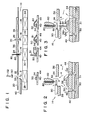
- Figs. 2 to 6 are partially enlarged sectional views, respectively, of the same.
- a convey path 10 for a lead frame 40 is constituted by a substantially cylindrical cover 20. Only an upper plate of the cover 20 is shown in Fig. 1.
- a die bonding portion 12, a wire bonding portion 14, a postbonding portion 16 and a postbaking portion 18 are arranged in the convey path 10 along a convey direction (indicated by arrow 2) of the lead frame 40 in the order named.
- Windows 22, 24 and 26 are formed in the upper plate of the cover 20 so as to correspond to the portions 12, 14 and 16, respectively.
- Heater blocks 28, 30, 32 and 34 for heating the lead frame 40 are provided to the convey path 10 to correspond to the portions 12, 14, 16 and 18, respectively.
- a gas path (see a gas path 31 in Fig. 2) for introducing a reducing gas to the path 10 is formed in each of the heater blocks 28, 30, 32 and 34.
- the reducing gas can be obtained by, e.g., mixing 10 % by volume of H 2 gas with N 2 gas.
- the reducing gas is supplied to the convey path 10 through the gas path.
- a gas introducing member 36 is arranged on the upper plate of the cover 20 of the convey path 10 between the portions 14 and 16.
- Another gas introducing member 38 is arranged on the upper plate of the cover 20 of the convey path 10 to correspond to the portion 18.
- gas paths 37 and 39 are formed in the members 36 and 38, respectively.
- the reducing gas obtained by mixing H 2 gas with N 2 gas is supplied to the convey path 10 through the gas paths 37 and 39 of the members 36 and 38, respectively. In this manner, the interior of the convey path 10 is filled with a reducing gas, e. g. , N 2 + 10 %H L .
- a collet 52 capable of clamping a semiconductor pellet (semiconductor element) 50 is provided at a position corresponding to the portion 12 so as to be capable of approaching and withdrawing from the convey path 10.
- the collet 52 can be inserted in the convey path 10 through the window 22 in the portion 12.
- the pellet 50 is supplied to the convey path 10 through the collet 52.
- a capillary 60 can clamp a bonding wire 80 and is arranged in the vicinity of the portion 14 so as to be capable of approaching and withdrawing from the convey path 10.
- the capillary 60 can be inserted in the convey path 10 through the window 24 in the portion 14.
- the bonding wire 80 is supplied to the convey path by the capillary 60.
- the bonding wire 80 is made of copper such as oxygen free copper and phosphor deoxidized copper, or a copper alloy such as Cu-20%Au.
- a compressing member 70 for thermocompressing the bonding wire 80 to an outer lead of the lead frame 40 is arranged at a position to correspond to the portion 16. The compressing member 70 can be inserted in and escape from the convey path 10 through the window 26 in the portion 16.
- a guide rail extends along a direction indicated by arrow 2 on the bottom of the convey path 10.
- the lead frame 40 is conveyed along the direction indicated by arrow 2 on the guide rail.
- the lead frame 40 is made of copper such as oxygen free copper and phosphor deoxidized copper, or a copper alloy.
- a mount portion 46 for the semiconductor pellet and an outer lead 44 are formed on the lead frame 40, as shown in detail in Fig. 7.
- the gas path 31 is formed in the heater block 30 to receive the reducing gas from a supply source.
- the reducing gas is discharged to the convey path 10 through a gap 42 between the mount portion 46 for the semiconductor pellet and the outer lead 44 formed on the lead frame 40.
- the remaining heater blocks 28, 32 and 34 have similar structures to that of the heater block 30. In the heater blocks 28, 32 and 34, the reducing gas is introduced to the convey path 10 from the gas path 31 directly or through the gap 42.
- a burner 90 is arranged outside the cover 20 and in the vicinity of the window 24 through which the capillary 60 provided at the portion 14 is inserted.
- the burner 90 comprises an inner tube 92 and an outer tube 94 coaxially surrounding it.
- the outer tube 94 has a distal end slightly projecting from the inner tube 92.
- a gas mixture of H 2 and 0 2 is sprayed from the tube 92 to form an oxyhydrogen torch 100.
- a lower end of the bonding wire 80 is heated by the torch 100 to, e.g., 1,000°C or higher and melted, thereby forming a ball 82.
- a gas mixture of 0 2 and N 2 gases is discharged from a space 96 between the tubes 94 and 92 to form an air curtain 102 around the torch 100.
- a peripheral portion of the cover 20 defining the window 24 is movable so as to change the opening area of the window 24.
- movable portions 36 are actuated to decrease the opening area of the window 24, only a portion near a distal end of the wire 80 is surrounded by the portions 36.
- the reducing gas is supplied to the convey path 10 through the gas path 31 in the heater block 30, the reducing gas flows as indicated by arrow 4 through the window 24 having a small opening area, and the space surrounding the lower end of the wire 80 is set in a reducing gas atmosphere.
- the lead frame 40 is conveyed on the guide rail (not shown) along the direction indicated by arrow 2, and stopped at the portion 12.
- the lead frame 40 is heated by the heater block 28 to about 400°C.
- the semiconductor pellet 50 clamped by the collet 52 is guided into the convey path 10 through the window 22.
- Solder is applied by an appropriate means to a lower surface of the pellet 50.
- the pellet 50 is then mounted on the mount portion of the lead frame 40 through a solder layer 54. Thereafter, the lead frame 40 is moved along the direction indicated by arrow 2, and stopped at the portion 14 as shown in Fig. 2.
- the lead frame 40 is heated by the heater block 30 to about 300°C.
- the pellet 50 on the lead frame 40 has an'electrode pad 56 formed thereon.
- the pad 56 is also heated by the heater block 30 to about 300°C.
- the capillary 60 is moved downward together with the wire 80 to an inlet port of the convey path 10 in the vicinity of the window 24.
- a gas mixture of H 2 and 0 2 gases is sprayed from the tube 92 of the burner 90 to form the torch 100.
- a gas mixture of 0 2 and N 2 gases is sprayed from a space 96 between the tubes 94 and 92 to form the curtain 102 around the torch 100.
- a reducing gas obtained by mixing H 2 and N 2 gases is supplied to the convey path 10 through the gas path 31 in the heater block 30.
- the reducing gas is heated to 200°C or higher by the heater block 30.
- the movable portions 36 are moved to decrease the opening area of the window 24.
- the reducing gas flows in the convey path 10 along a direction indicated by arrow 4 to surround the lower end portion of the wire 80 and the torch 100. In this manner, in a high-temperature reducing gas atmosphere, the lower end portion of the wire is heated and melted by the torch 100 to form the ball 82. Therefore, the copper is not subjected to oxidation, thus preventing a bonding failure.
- the mixing ratio of H 2 gas to N 2 gas of the reducing gas is preferably selected to be 5 to 20 % and 95 to 80 % by volume, respectively.
- the amount of the H 2 gas may be increased.
- the mixing ratio is preferably set in the range described above.
- a gas discharge port 48 can be provided in the vicinity of the portions 14, 16 and 18 of the heater blocks 30, 32 and 34, respectively, and the reducing gas can be supplied to the convey path 10 through each port 48.
- a gas mixture obtained by mixing the H 2 and 0 2 gases in the volume ratio of 2 : 1 is preferably sprayed from the tube 92 to form the torch 100. Meanwhile, a gas mixture of the 0 2 and N 2 gases is sprayed from the space between the tubes 94 and 92 to form the curtain 102.
- the air curtain 102 is formed to prevent the torch 100 from being extinguished due to the reducing atmosphere of the portion 14.
- the mixing ratio of the gas mixture to form the curtain 102 is preferably selected to be 20 to 100 % (0 2 gas) and 80 to 0 % (N 2 gas). If the amount of the 0 2 gas is excessive, the portion 14 (around the lower end portion of the wire 80) cannot be kept in a reducing gas atmosphere.
- Fig. 9B is a graph of the occurrence rate of defective connections when the final product is subjected to a temperature cycling test.
- the diameter D of the bonding region shown in Fig. 9A is plotted along the abscissa and the occurrence rate of defective connections is plotted along the ordinate axis.
- Reference symbol d denotes the cross section diameter of the wire 80.
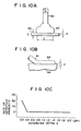
- the flat end portion of the ball 82 preferably extends into the pad 56 to a depth of 0.4 to 3 ⁇ m.
- reference symbol X denotes a depth to which the ball 82 extends into the pad 56 having thickness Y.
- Fig. 10C is a graph showing a relationship between the extending depth X of the ball 82 and the occurrence rate of defective products when the final products are subjected to the temperature cycling test. As apparent from Fig. 10C, when the depth X is 0.4 ⁇ m or more, the occurrence rate of defective products becomes substantially zero. For this reason, the flat end portion of the ball 82 is set to extend into the pad 56 to a depth of 0.4 ⁇ m or more.
- the pad 56 comprises an aluminum layer having a thickness of 1 to 3 ⁇ m and the wire 80 comprises a copper wire having a diameter of 25 ⁇ m
- a load of 50 to 100 g can be applied to the wire 80 so that depth X becomes 0.5 to 2.5 ⁇ m.
- Fig. 11 is a graph showing a relationship between the thickness of the pad and the occurrence rate of defective products.
- the thickness of the pad 56 is plotted along the abscissa and the occurrence rate of defective products is plotted along the ordinate axis.
- the thickness of the pad 56 is set to be 1 ⁇ m or more, the occurrence rate of defective products can be decreased to substantially zero.
- the wire 80 is fused by the oxyhydrogen torch of the burner 90 at a predetermined length as shown in Fig. 3.
- balls 82 and 84 are formed at distal ends of a wire 81 connected to the pad 56 and the wire 80 left in the capillary 60, respectively.
- the wires 80 and 81 are surrounded by the reducing gas during this fusing.
- the wire 81 is bent by an appropriate means (not shown) to a side of the outer lead 44 of the lead frame 40 as shown in Fig. 4.
- the lead frame 40 is then moved from the portion 14 to the portion 16.
- the temperature of the reducing gas in the convey path 10 is kept at 200 to-300°C, thereby keeping the wire 81 in the reducing atmosphere.
- the lead frame is then stopped at the portion 16 as shown in Fig. 5.
- the heater block 32 heats the lead frame 40 to about 300°C or higher.
- the compressing member 70 is moved downward and inserted in the convey path 10 through the window 26.
- the member 70 thermo- compresses the ball 84 of the wire 81 against the outer lead 44 made of copper or copper alloy.
- a load of 300 to 500 g is preferably applied thereto so that the ball 84 extends into the outer lead 44 to a depth of 20 to 50 um (indicated by Z in Fig. 10B) as shown in Fig. 10B.
- thermocompressing the ball 84 of the wire 81 to the outer lead to the depth as described the occurrence rate of defective products can be reduced to substantially zero.
- the wire 81, the ball 84 and the member 70 are surrounded by the reducing gas during this postbonding.
- the lead frame 40 is conveyed to the portion 18 and heated by the heater block 34 to about 300°C or higher, thereby being baked.
- the reducing gas is supplied to the convey path 10 through the gas path 35 in the heater block 34, and simultaneously the reducing gas is blown into the convey path 10 through the path 39 in the gas introducing member 38.
- the semiconductor pellet 50, the wire 81 and lead frame 40 are also kept in the reducing atmosphere at the portion 18.
- the bonding wire 81 is looped between the pad 56 of the pellet 50 and the outer lead 44 of the lead frame 40 as shown in Fig. 7.
- a single wire is shown in Figs. 1 to 6, two bonding wires are looped in practice as shown in Fig. 7.
- a bonding wire made of copper or a copper alloy is used so that various above-mentioned drawbacks inherent in bonding using a gold wire can be prevented.
- the bonding wire can be securely connected, and degradation in electrical characteristics at the connecting portion can be decreased to a minimum.
- the bonding wire can be fused not only by using the oxyhydrogen torch as in the embodiment described above but also by using a laser or electric torch.
- the ball can be formed at each of the cut ends of the bonding wire not only by the ball to ball method but also by cutting the bonding wire by a wedge of the capillary.
- Fig. 12 is a graph showing the occurrence rate of defective products according to the embodiment of the present invention together with that according to a conventional apparatus.
- the exposure time is plotted along the abscissa and the occurrence rate of defective products is plotted along the ordinate axis.
- the bonding wire is made of gold and the diameter of the bonding region of the ball and the electrode pad is 1/2 that of the cross section of the bonding wire.
- the other conditions are the same as in the embodiment of the present invention.
- 25 % of the final products became defective after 100 hours, and substantially 50 % became defective after 200 hours.
- the occurrence rate of defective products was substantially zero even after 200 hours.
- the temperature cycling test was performed for the semiconductor devices manufactured by the apparatus of the embodiment of the present invention and the conventional method. Also, the mechanical strength test was performed for the looped bonding wire of the devices manufactured by both apparatuses. In the temperature cycling test, the semiconductor device according to the preset invention exhibited a performance considerably superior to that of the conventional apparatus as a comparative example. In the mechanical strength (tensile strength) test, the bonding wire made of a copper alloy according to the present invention exhibited a strength 2 to 2.5 times that of the bonding wire made of gold as a comparative example.
Landscapes
- Engineering & Computer Science (AREA)
- Mechanical Engineering (AREA)
- Manufacturing & Machinery (AREA)
- Microelectronics & Electronic Packaging (AREA)
- Wire Bonding (AREA)
Applications Claiming Priority (6)
| Application Number | Priority Date | Filing Date | Title |
|---|---|---|---|
| JP15559184A JPS6135545A (ja) | 1984-07-27 | 1984-07-27 | 半導体装置の製造方法 |
| JP155591/84 | 1984-07-27 | ||
| JP219903/84 | 1984-10-19 | ||
| JP59219903A JPS6197938A (ja) | 1984-10-19 | 1984-10-19 | 半導体素子の組立方法 |
| JP59219902A JPS6197937A (ja) | 1984-10-19 | 1984-10-19 | 半導体素子の組立方法及びその装置 |
| JP219902/84 | 1984-10-19 |
Publications (3)
| Publication Number | Publication Date |
|---|---|
| EP0169574A2 true EP0169574A2 (fr) | 1986-01-29 |
| EP0169574A3 EP0169574A3 (en) | 1987-04-08 |
| EP0169574B1 EP0169574B1 (fr) | 1990-04-25 |
Family
ID=27320856
Family Applications (1)
| Application Number | Title | Priority Date | Filing Date |
|---|---|---|---|
| EP85109406A Expired - Lifetime EP0169574B1 (fr) | 1984-07-27 | 1985-07-26 | Appareil pour la fabrication d'un dispositif semi-conducteur |
Country Status (3)
| Country | Link |
|---|---|
| US (1) | US4732313A (fr) |
| EP (1) | EP0169574B1 (fr) |
| DE (1) | DE3577371D1 (fr) |
Cited By (8)
| Publication number | Priority date | Publication date | Assignee | Title |
|---|---|---|---|---|
| DE3641689A1 (de) * | 1985-12-24 | 1987-06-25 | Mitsubishi Electric Corp | Verfahren zur herstellung eines halbleiterbauelements und eines darin verwendeten halbleiterchips |
| DE3915472A1 (de) * | 1988-06-02 | 1989-12-07 | Samsung Electronics Co Ltd | Antioxidationssystem eines kupferdraht verwendenden wire-bonders |
| DE4317131A1 (de) * | 1992-05-22 | 1993-11-25 | Rohm Co Ltd | Verfahren und Vorrichtung zur Durchführung eines drahtkontaktierens unter Verwendung von Lötdraht |
| US5302550A (en) * | 1985-12-24 | 1994-04-12 | Mitsubishi Denki Kabushiki Kaisha | Method of bonding a microelectronic device |
| DE4417419A1 (de) * | 1993-05-21 | 1994-11-24 | Rohm Co Ltd | Verfahren zur Bildung eines Kugelendes für einen Lötdraht |
| DE4433503A1 (de) * | 1993-09-21 | 1995-03-23 | Rohm Co Ltd | Halbleiterbauelement mit Halbleiterchip und Verfahren zu dessen Herstellung |
| US5644281A (en) * | 1992-04-07 | 1997-07-01 | Rohm Co., Ltd. | Electronic component incorporating solder fuse wire |
| WO2002027781A1 (fr) * | 2000-09-29 | 2002-04-04 | Asm Technology Singapore Pte Ltd. | Procede de formage de bille |
Families Citing this family (40)
| Publication number | Priority date | Publication date | Assignee | Title |
|---|---|---|---|---|
| US5917707A (en) | 1993-11-16 | 1999-06-29 | Formfactor, Inc. | Flexible contact structure with an electrically conductive shell |
| US5476211A (en) * | 1993-11-16 | 1995-12-19 | Form Factor, Inc. | Method of manufacturing electrical contacts, using a sacrificial member |
| JPS63114138A (ja) * | 1986-10-31 | 1988-05-19 | Hitachi Ltd | ワイヤ積層ボンデイング方法 |
| US5189507A (en) * | 1986-12-17 | 1993-02-23 | Raychem Corporation | Interconnection of electronic components |
| US4955523A (en) * | 1986-12-17 | 1990-09-11 | Raychem Corporation | Interconnection of electronic components |
| US4976393A (en) * | 1986-12-26 | 1990-12-11 | Hitachi, Ltd. | Semiconductor device and production process thereof, as well as wire bonding device used therefor |
| JPH01143126U (fr) * | 1988-03-23 | 1989-10-02 | ||
| US4858819A (en) * | 1988-03-29 | 1989-08-22 | Hughes Aircraft Company | Orthogonal bonding method and equipment |
| JPH0793337B2 (ja) * | 1988-07-04 | 1995-10-09 | 株式会社新川 | ワーク加熱送り装置 |
| US5062565A (en) * | 1990-07-13 | 1991-11-05 | Micron Technology, Inc. | Method for combining die attach and wirebond in the assembly of a semiconductor package |
| US20050062492A1 (en) * | 2001-08-03 | 2005-03-24 | Beaman Brian Samuel | High density integrated circuit apparatus, test probe and methods of use thereof |
| US5820014A (en) | 1993-11-16 | 1998-10-13 | Form Factor, Inc. | Solder preforms |
| US7073254B2 (en) | 1993-11-16 | 2006-07-11 | Formfactor, Inc. | Method for mounting a plurality of spring contact elements |
| US7200930B2 (en) * | 1994-11-15 | 2007-04-10 | Formfactor, Inc. | Probe for semiconductor devices |
| US6442831B1 (en) | 1993-11-16 | 2002-09-03 | Formfactor, Inc. | Method for shaping spring elements |
| US20070228110A1 (en) * | 1993-11-16 | 2007-10-04 | Formfactor, Inc. | Method Of Wirebonding That Utilizes A Gas Flow Within A Capillary From Which A Wire Is Played Out |
| US7084656B1 (en) | 1993-11-16 | 2006-08-01 | Formfactor, Inc. | Probe for semiconductor devices |
| US20020053734A1 (en) | 1993-11-16 | 2002-05-09 | Formfactor, Inc. | Probe card assembly and kit, and methods of making same |
| US6835898B2 (en) * | 1993-11-16 | 2004-12-28 | Formfactor, Inc. | Electrical contact structures formed by configuring a flexible wire to have a springable shape and overcoating the wire with at least one layer of a resilient conductive material, methods of mounting the contact structures to electronic components, and applications for employing the contact structures |
| US6836962B2 (en) | 1993-11-16 | 2005-01-04 | Formfactor, Inc. | Method and apparatus for shaping spring elements |
| KR100517256B1 (ko) * | 1994-11-15 | 2005-12-16 | 폼팩터, 인크. | 가요성와이어로부터전기접점구조물의제조 |
| AU4160096A (en) | 1994-11-15 | 1996-06-06 | Formfactor, Inc. | Probe card assembly and kit, and methods of using same |
| US6727579B1 (en) | 1994-11-16 | 2004-04-27 | Formfactor, Inc. | Electrical contact structures formed by configuring a flexible wire to have a springable shape and overcoating the wire with at least one layer of a resilient conductive material, methods of mounting the contact structures to electronic components, and applications for employing the contact structures |
| US5842628A (en) | 1995-04-10 | 1998-12-01 | Fujitsu Limited | Wire bonding method, semiconductor device, capillary for wire bonding and ball bump forming method |
| US20100065963A1 (en) * | 1995-05-26 | 2010-03-18 | Formfactor, Inc. | Method of wirebonding that utilizes a gas flow within a capillary from which a wire is played out |
| JP3158338B2 (ja) * | 1995-09-18 | 2001-04-23 | 株式会社新川 | ボンデイング装置用加熱装置 |
| US5994152A (en) | 1996-02-21 | 1999-11-30 | Formfactor, Inc. | Fabricating interconnects and tips using sacrificial substrates |
| US8033838B2 (en) | 1996-02-21 | 2011-10-11 | Formfactor, Inc. | Microelectronic contact structure |
| US6180891B1 (en) | 1997-02-26 | 2001-01-30 | International Business Machines Corporation | Control of size and heat affected zone for fine pitch wire bonding |
| US6557253B1 (en) * | 1998-02-09 | 2003-05-06 | Tessera, Inc. | Method of making components with releasable leads |
| US6664628B2 (en) | 1998-07-13 | 2003-12-16 | Formfactor, Inc. | Electronic component overlapping dice of unsingulated semiconductor wafer |
| US6234376B1 (en) * | 1999-07-13 | 2001-05-22 | Kulicke & Soffa Investments, Inc. | Supplying a cover gas for wire ball bonding |
| US6759311B2 (en) | 2001-10-31 | 2004-07-06 | Formfactor, Inc. | Fan out of interconnect elements attached to semiconductor wafer |
| US20030146500A1 (en) * | 2002-02-04 | 2003-08-07 | Stmicroelectronics S.R.L. | Package for semiconductor device with ground lead connection having high stress resistance |
| US6945447B2 (en) * | 2002-06-05 | 2005-09-20 | Northrop Grumman Corporation | Thermal solder writing eutectic bonding process and apparatus |
| US8399972B2 (en) * | 2004-03-04 | 2013-03-19 | Skyworks Solutions, Inc. | Overmolded semiconductor package with a wirebond cage for EMI shielding |
| JP4014579B2 (ja) * | 2004-04-01 | 2007-11-28 | 沖電気工業株式会社 | ワイヤボンディング装置及びワイヤボンディング方法 |
| CN103311136A (zh) * | 2012-03-06 | 2013-09-18 | 深圳赛意法微电子有限公司 | 基于bga封装的铜线焊接装置及铜线焊接实现方法 |
| US20140246824A1 (en) * | 2013-03-02 | 2014-09-04 | Andrew P. Fiegener | Vise with Bi-directional Arms |
| JP2016028417A (ja) | 2014-07-11 | 2016-02-25 | ローム株式会社 | 電子装置 |
Family Cites Families (12)
| Publication number | Priority date | Publication date | Assignee | Title |
|---|---|---|---|---|
| US3051026A (en) * | 1959-02-19 | 1962-08-28 | Motorola Inc | Micromanipulator |
| US3102331A (en) * | 1960-07-21 | 1963-09-03 | Motorola Inc | Feeding and positioning apparatus |
| US3617682A (en) * | 1969-06-23 | 1971-11-02 | Gen Electric | Semiconductor chip bonder |
| DE2618867C2 (de) * | 1976-02-28 | 1985-09-05 | Telefunken electronic GmbH, 7100 Heilbronn | Verfahren zum Thermokompressions-Verbinden von auf Halbleiterkörpern befindlichen Metallanschlußkontakten |
| DE2608250C3 (de) * | 1976-02-28 | 1985-06-05 | Telefunken electronic GmbH, 7100 Heilbronn | Verfahren zum Thermokompressions-Verbinden von auf Halbleiterkörpern befindlichen Metall-Anschlußkontakten mit zugeordneten Gehäuseanschlußteilen und Vorrichtung zur Durchführung des Verfahrens |
| US4166562A (en) * | 1977-09-01 | 1979-09-04 | The Jade Corporation | Assembly system for microcomponent devices such as semiconductor devices |
| FR2412943A1 (fr) * | 1977-12-20 | 1979-07-20 | Thomson Csf | Procede de realisation de connexions d'un dispositif semi-conducteur sur embase, appareil pour la mise en oeuvre du procede, et dispositif semi-conducteur obtenu par ce procede |
| US4340166A (en) * | 1978-11-22 | 1982-07-20 | Kulicke & Soffa Industries, Inc. | High speed wire bonding method |
| JPS5713747A (en) * | 1980-06-27 | 1982-01-23 | Mitsubishi Electric Corp | Manufacture of semiconductor device |
| JPS5753954A (en) * | 1980-09-17 | 1982-03-31 | Toshiba Corp | Nail head bonding device |
| JPS58169918A (ja) * | 1982-03-31 | 1983-10-06 | Hitachi Ltd | ワイヤボンダ |
| US4476365A (en) * | 1982-10-08 | 1984-10-09 | Fairchild Camera & Instrument Corp. | Cover gas control of bonding ball formation |
-
1985
- 1985-07-26 EP EP85109406A patent/EP0169574B1/fr not_active Expired - Lifetime
- 1985-07-26 US US06/759,273 patent/US4732313A/en not_active Expired - Lifetime
- 1985-07-26 DE DE8585109406T patent/DE3577371D1/de not_active Expired - Lifetime
Cited By (14)
| Publication number | Priority date | Publication date | Assignee | Title |
|---|---|---|---|---|
| US5302550A (en) * | 1985-12-24 | 1994-04-12 | Mitsubishi Denki Kabushiki Kaisha | Method of bonding a microelectronic device |
| DE3641689A1 (de) * | 1985-12-24 | 1987-06-25 | Mitsubishi Electric Corp | Verfahren zur herstellung eines halbleiterbauelements und eines darin verwendeten halbleiterchips |
| DE3915472A1 (de) * | 1988-06-02 | 1989-12-07 | Samsung Electronics Co Ltd | Antioxidationssystem eines kupferdraht verwendenden wire-bonders |
| GB2220101A (en) * | 1988-06-02 | 1989-12-28 | Samsung Electronics Co Ltd | Wire bonding |
| GB2220101B (en) * | 1988-06-02 | 1992-09-09 | Samsung Electronics Co Ltd | Wire bonding |
| US5644281A (en) * | 1992-04-07 | 1997-07-01 | Rohm Co., Ltd. | Electronic component incorporating solder fuse wire |
| US5395037A (en) * | 1992-04-22 | 1995-03-07 | Rohm Co., Ltd. | Method and apparatus for performing wire bonding by using solder wire |
| DE4317131A1 (de) * | 1992-05-22 | 1993-11-25 | Rohm Co Ltd | Verfahren und Vorrichtung zur Durchführung eines drahtkontaktierens unter Verwendung von Lötdraht |
| DE4417419A1 (de) * | 1993-05-21 | 1994-11-24 | Rohm Co Ltd | Verfahren zur Bildung eines Kugelendes für einen Lötdraht |
| US5431329A (en) * | 1993-05-21 | 1995-07-11 | Rohm Co., Ltd. | Method of forming a ball end for a solder wire |
| DE4417419C2 (de) * | 1993-05-21 | 2000-11-02 | Rohm Co Ltd | Verfahren zur Formung einer Kugel an einem Lötdraht |
| DE4433503A1 (de) * | 1993-09-21 | 1995-03-23 | Rohm Co Ltd | Halbleiterbauelement mit Halbleiterchip und Verfahren zu dessen Herstellung |
| DE4433503C2 (de) * | 1993-09-21 | 2001-04-26 | Rohm Co Ltd | Verfahren zum Herstellen eines Halbleiterbauelements |
| WO2002027781A1 (fr) * | 2000-09-29 | 2002-04-04 | Asm Technology Singapore Pte Ltd. | Procede de formage de bille |
Also Published As
| Publication number | Publication date |
|---|---|
| US4732313A (en) | 1988-03-22 |
| EP0169574B1 (fr) | 1990-04-25 |
| DE3577371D1 (de) | 1990-05-31 |
| EP0169574A3 (en) | 1987-04-08 |
Similar Documents
| Publication | Publication Date | Title |
|---|---|---|
| EP0169574B1 (fr) | Appareil pour la fabrication d'un dispositif semi-conducteur | |
| US6455785B1 (en) | Bump connection with stacked metal balls | |
| KR100334993B1 (ko) | 히터 | |
| US4705204A (en) | Method of ball forming for wire bonding | |
| US6271601B1 (en) | Wire bonding method and apparatus and semiconductor device | |
| US3384283A (en) | Vibratory wire bonding method and apparatus | |
| EP0178170B1 (fr) | Dispositif semi-conducteur ayant un fil de connexion et son procédé de fabrication | |
| US3742283A (en) | Press seal for lamp having fused silica envelope | |
| KR910000154B1 (ko) | 반도체장치와 그 재법 및 그것에 사용되는 본딩와이어 | |
| GB2151529A (en) | Method for making electrical contact to semiconductor devices | |
| JPS60227432A (ja) | ボンデイング用ワイヤのボ−ル形成装置 | |
| CA2145972C (fr) | Protecteur de circuit et methode de fabrication de ce protecteur | |
| KR19990006871A (ko) | 글래스내에서의 몰리부덴 박막 밀봉부와 이러한 몰리부덴 박막 밀봉부를 가지는 전기 램프 | |
| GB2171042A (en) | Wire bonder with controlled atmosphere | |
| US8604627B2 (en) | Semiconductor device | |
| KR900000205B1 (ko) | 결속상태가 개선된 반도체 장치의 제조장치 | |
| JP2535489B2 (ja) | 固体電解コンデンサ― | |
| KR900005348B1 (ko) | 반도체장치의 제조방법 | |
| US20250140739A1 (en) | Laser enhanced wire bonding for semiconductor device packages | |
| JPS6355946A (ja) | ワイヤボンダにおけるボ−ル形成方法 | |
| JPH0462456B2 (fr) | ||
| JPH0354855B2 (fr) | ||
| JP2003188329A (ja) | 電力用半導体装置のゲート端子の構成部材間接続方法 | |
| EP1220391A1 (fr) | Empaquetage comprenant un refroidisseur thermo-électrique | |
| JPH08125099A (ja) | 半導体装置の製造方法 |
Legal Events
| Date | Code | Title | Description |
|---|---|---|---|
| PUAI | Public reference made under article 153(3) epc to a published international application that has entered the european phase |
Free format text: ORIGINAL CODE: 0009012 |
|
| 17P | Request for examination filed |
Effective date: 19850726 |
|
| AK | Designated contracting states |
Designated state(s): DE FR GB |
|
| PUAL | Search report despatched |
Free format text: ORIGINAL CODE: 0009013 |
|
| AK | Designated contracting states |
Kind code of ref document: A3 Designated state(s): DE FR GB |
|
| 17Q | First examination report despatched |
Effective date: 19890109 |
|
| GRAA | (expected) grant |
Free format text: ORIGINAL CODE: 0009210 |
|
| AK | Designated contracting states |
Kind code of ref document: B1 Designated state(s): DE FR GB |
|
| REF | Corresponds to: |
Ref document number: 3577371 Country of ref document: DE Date of ref document: 19900531 |
|
| ET | Fr: translation filed | ||
| PLBE | No opposition filed within time limit |
Free format text: ORIGINAL CODE: 0009261 |
|
| STAA | Information on the status of an ep patent application or granted ep patent |
Free format text: STATUS: NO OPPOSITION FILED WITHIN TIME LIMIT |
|
| 26N | No opposition filed | ||
| PGFP | Annual fee paid to national office [announced via postgrant information from national office to epo] |
Ref country code: FR Payment date: 19970709 Year of fee payment: 13 |
|
| PGFP | Annual fee paid to national office [announced via postgrant information from national office to epo] |
Ref country code: DE Payment date: 19970801 Year of fee payment: 13 |
|
| REG | Reference to a national code |
Ref country code: GB Ref legal event code: 746 Effective date: 19981015 |
|
| PG25 | Lapsed in a contracting state [announced via postgrant information from national office to epo] |
Ref country code: FR Free format text: LAPSE BECAUSE OF NON-PAYMENT OF DUE FEES Effective date: 19990331 |
|
| PG25 | Lapsed in a contracting state [announced via postgrant information from national office to epo] |
Ref country code: DE Free format text: LAPSE BECAUSE OF NON-PAYMENT OF DUE FEES Effective date: 19990501 |
|
| REG | Reference to a national code |
Ref country code: FR Ref legal event code: ST |
|
| REG | Reference to a national code |
Ref country code: GB Ref legal event code: IF02 |
|
| PGFP | Annual fee paid to national office [announced via postgrant information from national office to epo] |
Ref country code: GB Payment date: 20040721 Year of fee payment: 20 |
|
| PG25 | Lapsed in a contracting state [announced via postgrant information from national office to epo] |
Ref country code: GB Free format text: LAPSE BECAUSE OF EXPIRATION OF PROTECTION Effective date: 20050725 |
|
| REG | Reference to a national code |
Ref country code: GB Ref legal event code: PE20 |