EP0171104A1 - Elément d'enregistrement optique - Google Patents
Elément d'enregistrement optique Download PDFInfo
- Publication number
- EP0171104A1 EP0171104A1 EP85201067A EP85201067A EP0171104A1 EP 0171104 A1 EP0171104 A1 EP 0171104A1 EP 85201067 A EP85201067 A EP 85201067A EP 85201067 A EP85201067 A EP 85201067A EP 0171104 A1 EP0171104 A1 EP 0171104A1
- Authority
- EP
- European Patent Office
- Prior art keywords
- recording
- foil
- synthetic resin
- recording layers
- layers
- Prior art date
- Legal status (The legal status is an assumption and is not a legal conclusion. Google has not performed a legal analysis and makes no representation as to the accuracy of the status listed.)
- Withdrawn
Links
- 230000003287 optical effect Effects 0.000 title claims description 13
- 239000011888 foil Substances 0.000 claims abstract description 19
- 239000000758 substrate Substances 0.000 claims abstract description 19
- 229920003002 synthetic resin Polymers 0.000 claims abstract description 17
- 239000000057 synthetic resin Substances 0.000 claims abstract description 17
- 125000006850 spacer group Chemical group 0.000 description 8
- 239000000463 material Substances 0.000 description 7
- -1 for example Substances 0.000 description 4
- 229910001215 Te alloy Inorganic materials 0.000 description 3
- 229910052785 arsenic Inorganic materials 0.000 description 3
- 150000004770 chalcogenides Chemical class 0.000 description 3
- 230000002349 favourable effect Effects 0.000 description 3
- 239000007789 gas Substances 0.000 description 3
- 229910052745 lead Inorganic materials 0.000 description 3
- 230000035945 sensitivity Effects 0.000 description 3
- 229910052717 sulfur Inorganic materials 0.000 description 3
- IJGRMHOSHXDMSA-UHFFFAOYSA-N Atomic nitrogen Chemical compound N#N IJGRMHOSHXDMSA-UHFFFAOYSA-N 0.000 description 2
- 238000006243 chemical reaction Methods 0.000 description 2
- 229910052733 gallium Inorganic materials 0.000 description 2
- 229910052738 indium Inorganic materials 0.000 description 2
- 238000000034 method Methods 0.000 description 2
- 229920003229 poly(methyl methacrylate) Polymers 0.000 description 2
- 239000004417 polycarbonate Substances 0.000 description 2
- 229920000515 polycarbonate Polymers 0.000 description 2
- 239000004926 polymethyl methacrylate Substances 0.000 description 2
- 229920005989 resin Polymers 0.000 description 2
- 239000011347 resin Substances 0.000 description 2
- 229910052710 silicon Inorganic materials 0.000 description 2
- 229910052718 tin Inorganic materials 0.000 description 2
- 150000001252 acrylic acid derivatives Chemical class 0.000 description 1
- 238000004026 adhesive bonding Methods 0.000 description 1
- 229910045601 alloy Inorganic materials 0.000 description 1
- 239000000956 alloy Substances 0.000 description 1
- 229910052787 antimony Inorganic materials 0.000 description 1
- 230000015572 biosynthetic process Effects 0.000 description 1
- 229910052797 bismuth Inorganic materials 0.000 description 1
- 238000010276 construction Methods 0.000 description 1
- 230000001419 dependent effect Effects 0.000 description 1
- 238000006073 displacement reaction Methods 0.000 description 1
- 239000003292 glue Substances 0.000 description 1
- 239000011261 inert gas Substances 0.000 description 1
- 238000001746 injection moulding Methods 0.000 description 1
- 239000011159 matrix material Substances 0.000 description 1
- 239000002184 metal Substances 0.000 description 1
- 229910052751 metal Inorganic materials 0.000 description 1
- 229910052757 nitrogen Inorganic materials 0.000 description 1
- 238000005457 optimization Methods 0.000 description 1
- 229920000728 polyester Polymers 0.000 description 1
- 239000004800 polyvinyl chloride Substances 0.000 description 1
- 229920000915 polyvinyl chloride Polymers 0.000 description 1
- 229910052712 strontium Inorganic materials 0.000 description 1
- 229910052714 tellurium Inorganic materials 0.000 description 1
- 229910052716 thallium Inorganic materials 0.000 description 1
- 238000007669 thermal treatment Methods 0.000 description 1
- 238000003466 welding Methods 0.000 description 1
Images
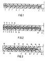
Classifications
-
- G—PHYSICS
- G11—INFORMATION STORAGE
- G11B—INFORMATION STORAGE BASED ON RELATIVE MOVEMENT BETWEEN RECORD CARRIER AND TRANSDUCER
- G11B7/00—Recording or reproducing by optical means, e.g. recording using a thermal beam of optical radiation by modifying optical properties or the physical structure, reproducing using an optical beam at lower power by sensing optical properties; Record carriers therefor
- G11B7/24—Record carriers characterised by shape, structure or physical properties, or by the selection of the material
- G11B7/24015—Air-sandwiched discs
Landscapes
- Thermal Transfer Or Thermal Recording In General (AREA)
- Optical Record Carriers And Manufacture Thereof (AREA)
Applications Claiming Priority (2)
| Application Number | Priority Date | Filing Date | Title |
|---|---|---|---|
| NL8402193A NL8402193A (nl) | 1984-07-11 | 1984-07-11 | Optisch registratie element. |
| NL8402193 | 1984-07-18 |
Publications (1)
| Publication Number | Publication Date |
|---|---|
| EP0171104A1 true EP0171104A1 (fr) | 1986-02-12 |
Family
ID=19844202
Family Applications (1)
| Application Number | Title | Priority Date | Filing Date |
|---|---|---|---|
| EP85201067A Withdrawn EP0171104A1 (fr) | 1984-07-11 | 1985-07-03 | Elément d'enregistrement optique |
Country Status (4)
| Country | Link |
|---|---|
| US (1) | US4731780A (fr) |
| EP (1) | EP0171104A1 (fr) |
| JP (1) | JPS6134742A (fr) |
| NL (1) | NL8402193A (fr) |
Families Citing this family (2)
| Publication number | Priority date | Publication date | Assignee | Title |
|---|---|---|---|---|
| DE3885156T2 (de) * | 1987-06-11 | 1994-03-17 | Asahi Chemical Ind | Verfahren zum Aufzeichnen und Löschen von Daten. |
| US5538774A (en) * | 1994-07-29 | 1996-07-23 | Minnesota Mining And Manufacturing Company | Internally damped rotatable storage article |
Citations (4)
| Publication number | Priority date | Publication date | Assignee | Title |
|---|---|---|---|---|
| DE2618773A1 (de) * | 1976-04-29 | 1977-11-10 | Licentia Gmbh | Aufzeichnungstraeger mit schutzschicht |
| EP0049821A1 (fr) * | 1980-10-09 | 1982-04-21 | Kabushiki Kaisha Toshiba | Elément d'enregistrement de données |
| EP0049813A1 (fr) * | 1980-10-09 | 1982-04-21 | Kabushiki Kaisha Toshiba | Elément d'enregistrement de données et procédé de fabrication correspondant |
| EP0063439A1 (fr) * | 1981-04-10 | 1982-10-27 | Sony Corporation | Support d'enregistrement à lire par voie optique |
Family Cites Families (4)
| Publication number | Priority date | Publication date | Assignee | Title |
|---|---|---|---|---|
| US4441179A (en) * | 1979-01-15 | 1984-04-03 | Discovision Associates | Optical video disc structure |
| US4363844A (en) * | 1980-09-22 | 1982-12-14 | Lewis Terry W | Metallized information carrying discs |
| JPS5835741A (ja) * | 1981-08-21 | 1983-03-02 | Hitachi Ltd | プラスチツク情報記録媒体 |
| JPS58137147A (ja) * | 1982-02-08 | 1983-08-15 | Sony Corp | 情報記録媒体 |
-
1984
- 1984-07-11 NL NL8402193A patent/NL8402193A/nl unknown
-
1985
- 1985-07-03 EP EP85201067A patent/EP0171104A1/fr not_active Withdrawn
- 1985-07-09 JP JP14936885A patent/JPS6134742A/ja active Pending
-
1987
- 1987-01-21 US US07/004,320 patent/US4731780A/en not_active Expired - Fee Related
Patent Citations (4)
| Publication number | Priority date | Publication date | Assignee | Title |
|---|---|---|---|---|
| DE2618773A1 (de) * | 1976-04-29 | 1977-11-10 | Licentia Gmbh | Aufzeichnungstraeger mit schutzschicht |
| EP0049821A1 (fr) * | 1980-10-09 | 1982-04-21 | Kabushiki Kaisha Toshiba | Elément d'enregistrement de données |
| EP0049813A1 (fr) * | 1980-10-09 | 1982-04-21 | Kabushiki Kaisha Toshiba | Elément d'enregistrement de données et procédé de fabrication correspondant |
| EP0063439A1 (fr) * | 1981-04-10 | 1982-10-27 | Sony Corporation | Support d'enregistrement à lire par voie optique |
Non-Patent Citations (5)
| Title |
|---|
| PATENTS ABSTRACTS OF JAPAN, vol. 3, no. 56 (E-110), 15th May 1979, page 157 E 110; & JP - A - 54 35 707 (HITACHI SEISAKUSHO K.K.) 16-03-1979 * |
| PATENTS ABSTRACTS OF JAPAN, vol. 3, no. 78 (E-121), 5th July 1979, page 12 E 121; & JP - A - 54 55 445 (CANON K.K.) 05-02-1979 * |
| PATENTS ABSTRACTS OF JAPAN, vol. 7, no. 120 (M-217)[1265], 25th May 1983, page 155 M 217; & JP - A - 58 39 493 (FUJI SHASHIN FILM K.K.) 08-03-1983 * |
| PATENTS ABSTRACTS OF JAPAN, vol. 7, no. 278 (P-242)[1423], 10th December 1983, page 128 P 242; & JP - A - 58 155 545 (TOKYO SHIBAURA DENKI K.K.) 16-09-1983 * |
| PATENTS ABSTRACTS OF JAPAN, vol. 7, no. 70 (P-185)[1215], 23rd March 1983, page 49 P 185; & JP - A - 57 212 637 (RICOH K.K.) 27-12-1982 * |
Also Published As
| Publication number | Publication date |
|---|---|
| US4731780A (en) | 1988-03-15 |
| NL8402193A (nl) | 1986-02-03 |
| JPS6134742A (ja) | 1986-02-19 |
Similar Documents
| Publication | Publication Date | Title |
|---|---|---|
| US4385303A (en) | Optical recording and reproducing disc | |
| KR100776850B1 (ko) | 광 기록 매체 및 광 기록 재생 장치 | |
| EP0352105B1 (fr) | Milieu pour disque optique | |
| EP1184858A2 (fr) | Milieu d'enregistrement optique d'information et procédé d'enregistrement, lecture et effacement optique d'information | |
| CN1419693A (zh) | 光学信息媒体和制造该媒体的方法 | |
| EP0049813A1 (fr) | Elément d'enregistrement de données et procédé de fabrication correspondant | |
| US6128271A (en) | Optical recording medium | |
| EP0171104A1 (fr) | Elément d'enregistrement optique | |
| JP4080741B2 (ja) | 多層光記録媒体の製造方法および多層光記録媒体 | |
| EP0977189B1 (fr) | Procédé d'enregistrement optique | |
| KR100939850B1 (ko) | 광정보 기록매체, 그 광측정방법 및 광정보 기록/재생방법 | |
| KR19990023532A (ko) | 상변화 광디스크 매체 | |
| EP1564733B1 (fr) | Substrat de disque et disque optique | |
| US20020057646A1 (en) | Optical information recording medium and method of manufacturing the same | |
| US5851729A (en) | Optical disc | |
| JPS59101043A (ja) | 情報記録再生坦体 | |
| EP1229522B1 (fr) | Moyen d'enregistrement optique, substrat pour moyen d'enregistrement optique et dispositif a disque optique | |
| JPS61130094A (ja) | 情報記録媒体及び記録再生方法 | |
| KR101055130B1 (ko) | 광학적 정보기록매체 및 광학적 정보기록 재생시스템 | |
| JP3076585B2 (ja) | 光情報記録媒体 | |
| EP0329426B1 (fr) | Carte d'enregistrement optique et méthode de fabrication d'une telle carte | |
| JP2551995B2 (ja) | 光メモリ素子 | |
| KR100276461B1 (ko) | 광디스크의 기판 | |
| JPH02123535A (ja) | 光記録媒体 | |
| JPS61210546A (ja) | 記録媒体 |
Legal Events
| Date | Code | Title | Description |
|---|---|---|---|
| PUAI | Public reference made under article 153(3) epc to a published international application that has entered the european phase |
Free format text: ORIGINAL CODE: 0009012 |
|
| AK | Designated contracting states |
Designated state(s): DE FR GB IT NL |
|
| 17P | Request for examination filed |
Effective date: 19860804 |
|
| 17Q | First examination report despatched |
Effective date: 19871216 |
|
| STAA | Information on the status of an ep patent application or granted ep patent |
Free format text: STATUS: THE APPLICATION IS DEEMED TO BE WITHDRAWN |
|
| 18D | Application deemed to be withdrawn |
Effective date: 19880427 |
|
| RIN1 | Information on inventor provided before grant (corrected) |
Inventor name: KIVITS, PETRUS JOHANNES Inventor name: DUFOUR, RENE Inventor name: SENS, MARTINUS MARIA |