EP0171274A2 - Photovoltaic device having long term energy conversion stability and method of producing same - Google Patents
Photovoltaic device having long term energy conversion stability and method of producing same Download PDFInfo
- Publication number
- EP0171274A2 EP0171274A2 EP85305531A EP85305531A EP0171274A2 EP 0171274 A2 EP0171274 A2 EP 0171274A2 EP 85305531 A EP85305531 A EP 85305531A EP 85305531 A EP85305531 A EP 85305531A EP 0171274 A2 EP0171274 A2 EP 0171274A2
- Authority
- EP
- European Patent Office
- Prior art keywords
- layer
- semiconductor
- intrinsic
- photo
- annealing
- Prior art date
- Legal status (The legal status is an assumption and is not a legal conclusion. Google has not performed a legal analysis and makes no representation as to the accuracy of the status listed.)
- Granted
Links
Images

Classifications
-
- H—ELECTRICITY
- H10—SEMICONDUCTOR DEVICES; ELECTRIC SOLID-STATE DEVICES NOT OTHERWISE PROVIDED FOR
- H10F—INORGANIC SEMICONDUCTOR DEVICES SENSITIVE TO INFRARED RADIATION, LIGHT, ELECTROMAGNETIC RADIATION OF SHORTER WAVELENGTH OR CORPUSCULAR RADIATION
- H10F10/00—Individual photovoltaic cells, e.g. solar cells
- H10F10/10—Individual photovoltaic cells, e.g. solar cells having potential barriers
- H10F10/17—Photovoltaic cells having only PIN junction potential barriers
-
- H—ELECTRICITY
- H10—SEMICONDUCTOR DEVICES; ELECTRIC SOLID-STATE DEVICES NOT OTHERWISE PROVIDED FOR
- H10F—INORGANIC SEMICONDUCTOR DEVICES SENSITIVE TO INFRARED RADIATION, LIGHT, ELECTROMAGNETIC RADIATION OF SHORTER WAVELENGTH OR CORPUSCULAR RADIATION
- H10F77/00—Constructional details of devices covered by this subclass
- H10F77/10—Semiconductor bodies
- H10F77/16—Material structures, e.g. crystalline structures, film structures or crystal plane orientations
- H10F77/162—Non-monocrystalline materials, e.g. semiconductor particles embedded in insulating materials
- H10F77/166—Amorphous semiconductors
- H10F77/1662—Amorphous semiconductors including only Group IV materials
- H10F77/1668—Amorphous semiconductors including only Group IV materials presenting light-induced characteristic variations, e.g. Staebler-Wronski effect
-
- Y—GENERAL TAGGING OF NEW TECHNOLOGICAL DEVELOPMENTS; GENERAL TAGGING OF CROSS-SECTIONAL TECHNOLOGIES SPANNING OVER SEVERAL SECTIONS OF THE IPC; TECHNICAL SUBJECTS COVERED BY FORMER USPC CROSS-REFERENCE ART COLLECTIONS [XRACs] AND DIGESTS
- Y02—TECHNOLOGIES OR APPLICATIONS FOR MITIGATION OR ADAPTATION AGAINST CLIMATE CHANGE
- Y02E—REDUCTION OF GREENHOUSE GAS [GHG] EMISSIONS, RELATED TO ENERGY GENERATION, TRANSMISSION OR DISTRIBUTION
- Y02E10/00—Energy generation through renewable energy sources
- Y02E10/50—Photovoltaic [PV] energy
- Y02E10/548—Amorphous silicon PV cells
-
- Y—GENERAL TAGGING OF NEW TECHNOLOGICAL DEVELOPMENTS; GENERAL TAGGING OF CROSS-SECTIONAL TECHNOLOGIES SPANNING OVER SEVERAL SECTIONS OF THE IPC; TECHNICAL SUBJECTS COVERED BY FORMER USPC CROSS-REFERENCE ART COLLECTIONS [XRACs] AND DIGESTS
- Y10—TECHNICAL SUBJECTS COVERED BY FORMER USPC
- Y10S—TECHNICAL SUBJECTS COVERED BY FORMER USPC CROSS-REFERENCE ART COLLECTIONS [XRACs] AND DIGESTS
- Y10S136/00—Batteries: thermoelectric and photoelectric
- Y10S136/29—Testing, calibrating, treating, e.g. aging
Definitions
- Amorphous silicon alloys of electronic device quality can be prepared by glow discharge or vacuum deposition techniques. Such deposition techniques are described in U.S. Patent Nos. 4,226,898, 4,217,374, and 4,517,223 to Stanford R. Ovshinsky and others. As disclosed in those patents, fluorine introduced into the amorphous silicon semiconductor layers substantially reduces the density of the localized defect states and facilitates the addition of other alloying materials, such as germanium.
- amorphous silicon alloys can be deposited in multiple layers over large-area substrates to form solar cells in a high volume continuous processing system.
- Such continuous processing systems are disclosed in U.S. Patent Nos. 4,400,409, 4,410,588, 4,438,723 and 4,485,125.
- a substrate may be continuously advanced through a succession of deposition chambers, in each of which a layer of semiconductor material is deposited.
- the first chamber is dedicated to depositing a p-type semiconductor alloy
- the second chamber is dedicated to depositing an intrinsic amorphous semiconductor alloy
- the third chamber is dedicated to depositing an n-type semiconductor alloy.
- photo-degradation The performance of amorphous silicon-based photovoltaic devices has been observed to degrade during operation. This process, termed “photo-degradation”, or “Staebler-Wronski degradation” is believed to be caused by the breaking of weak bonds between atoms of the semiconductor material, resulting in the formation of defect states in the band gap. These photo-generated defects may be cured by annealing at elevated temperatures for a prolonged period of time, for example, a temperature of approximately 150°C for several hours.
- annealing may be carried out periodically or continuously to restore or maintain performance.
- a continuous annealing solar collector panel collects and retains solar thermal energy.
- the semiconductor material is maintained, during normal operation, at an elevated temperature (typically in excess of 100°C) and the defect states in the energy gap of the semiconductor material are annealed substantially simultaneously with their formation.
- elevated temperatures required by the known continuous annealing process limits its use. It is therefore desirable to lower the annealing temperature.
- the problem of using a high annealing temperature is solved in the invention by including small amounts of an annealing temperature reducing agent, typically a dopant, in the charge carrier generating region of a photovoltaic device.
- an annealing temperature reducing agent typically a dopant
- the inclusion of small amounts of a dopant, such as boron, in the intrinsic semiconductor layer has been found to reduce the annealing temperature to 100°C or lower.
- Other dopants such as aluminum, gallium, indium, thallium and combinations of them may also be used.
- the photovoltaic device is periodically raised to its annealing temperature by an electrical heater.
- the photovoltaic device includes a thermally insulated module that retains solar thermal energy either to raise the semiconductor material to its annealing temperature periodically or to maintain the semiconductor material at its annealing temperature constantly.
- FIG. 1 shows a p-i-n type photovoltaic device 10 made up of individual p-i-n type cells 12a, 12b, and 12c.
- a substrate 11 joins cell 12a and functions as an electrode of cell 10.
- Substrate 11 may be formed of a metallic material such as thin stainless steel or aluminum, or it may be formed from a thin electroformed member such as nickel. Alternatively, substrate 11 may be formed from an insulating material such as glass or synthetic polymers, with an electrically conductive electrode layer formed on it.
- the term, "substrate” as used here includes any such elements added by preliminary processing.
- Each of the cells, 12a, 12b, and 12c are fabricated from an amorphous semiconductor body containing at least silicon or germanium.
- Each of the semiconductor bodies includes an n-type conductivity semiconductor layer 20a, 20b, and 20c; a lightly doped intrinsic semiconductor layer 18a, 18b and 18c, in accord with the principles of the instant invention; and a p-type conductivity semiconductor layer 16a, 16b, and 16c.
- P-type layers 16 and n-type layers 20 cooperate to establish an electric field across intrinsic layers 18 for collection of charge carriers generated in layers 18 by light.
- a TCO (transparent conductive oxide) layer 22 formed in the preferred embodiment of indium tin oxide, is deposited on the layer of semiconductor material opposite substrate 11 and forms a second electrode.
- An electrode grid 24 may be applied to TCO layer 22 to increase current collection efficiency.
- photovoltaic cell illlustrated in Figure 1 is a stacked assembly of p-i-n cells
- the invention may also be employed with other cell arrangements such as single p-i-n cells, or stacked or single n-i-p or p-n cells.
- Applicants have shown analytically and confirmed experimentally that the incorporation of small amounts of selected annealing temperature reducing agents, such as, for example, p-dopants, into a host matrix of an intrinsic amorphous semiconductor results in a reduction in the temperature at which light-induced defects may be removed by annealing.
- the reduction in temperature annealing is independent of any particular device configuration in which the amorphous semiconductor may be used. Therefore, the improved amorphous semiconductor of the invention may be incorporated in a wide variety of photoresponsive devices, such as the tandem p-i-n type photovoltaic device described with reference to Figure 1.
- the improved amorphous semiconductor may be deposited by sputtering, in which case the annealing temperature reducing agent may be either present in solid form in the sputtering target, or introduced into the atmosphere in the deposition chamber in gaseous form. If introduced in an evaporation process, the annealing temperature reducing agent is either added to the solid being evaporated or added to the residual atmosphere in the deposition chamber. If chemical vapor deposition is employed for the fabrication of the amorphous semiconductor, the annealing temperature reducing agent is preferably added to the process gas stream. In an electroplating process, an appropriate amount of annealing temperature reducing agent is either added to the electrode from which the plated deposit is formed or is added directly to the plating bath. In a glow discharge process, the annealing temperature reducing agent is added to the process gas stream.
- Previously deposited layers of amorphous semiconductors may have an annealing temperature reducing agent introduced into them by ion implantation, post deposition treatment in an activated atmosphere of the annealing temperature reducing agent or a diffusion process.
- an intrinsic amorphous silicon:hydrogen alloy This intrinsic alloy is generally similar to that utilized in intrinsic layers, 18a, 18b and 18c of photovoltaic device 10 of Figure 1.
- a series of layers of an amorphous silicon:hydrogen alloy were deposited by a glow discharge process on Corning 7059 glass substrates maintained at 250°C. Silane was decomposed using radio frequency energy of 13.56 MHz. The decomposition was carried out at a pressure of approximately 27 pascal.
- Samples of a layer of an amorphous silicon:hydrogen alloy incorporating various levels of boron were prepared by adding differing small amounts of diborane to the chamber as the non-doped alloys were being deposited.
- Each of the samples was annealed at 200°C for two hours to remove any defects created during preparation of the samples.
- the annealed samples were then degraded by exposure to a white light flux of approximately 100mW/cm 2 for 2 hours. Photoconductivity of the degraded samples was then measured, the samples were next annealed at 100°C for 15 minutes and the photoconductivity measured again.
- the samples have a band gap of approximately 1.8 eV with the Fermi level located approximately 1.1 eV from the valence band (i.e., 0.7 eV from the conduction band), and therefore, are regarded as slightly n-type.
- annealing at 100°C for 15 minutes has virtually no effect upon light-induced defects.
- Applicants have found that the incorporation of a p-dopant, particularly boron, in amounts sufficient to shift the Fermi level of the intrinsic amorphous semiconductor alloy toward the valence band (thereby making the intrinsic semiconductor slightly p-type) results in an improvement in the annealing characteristics.
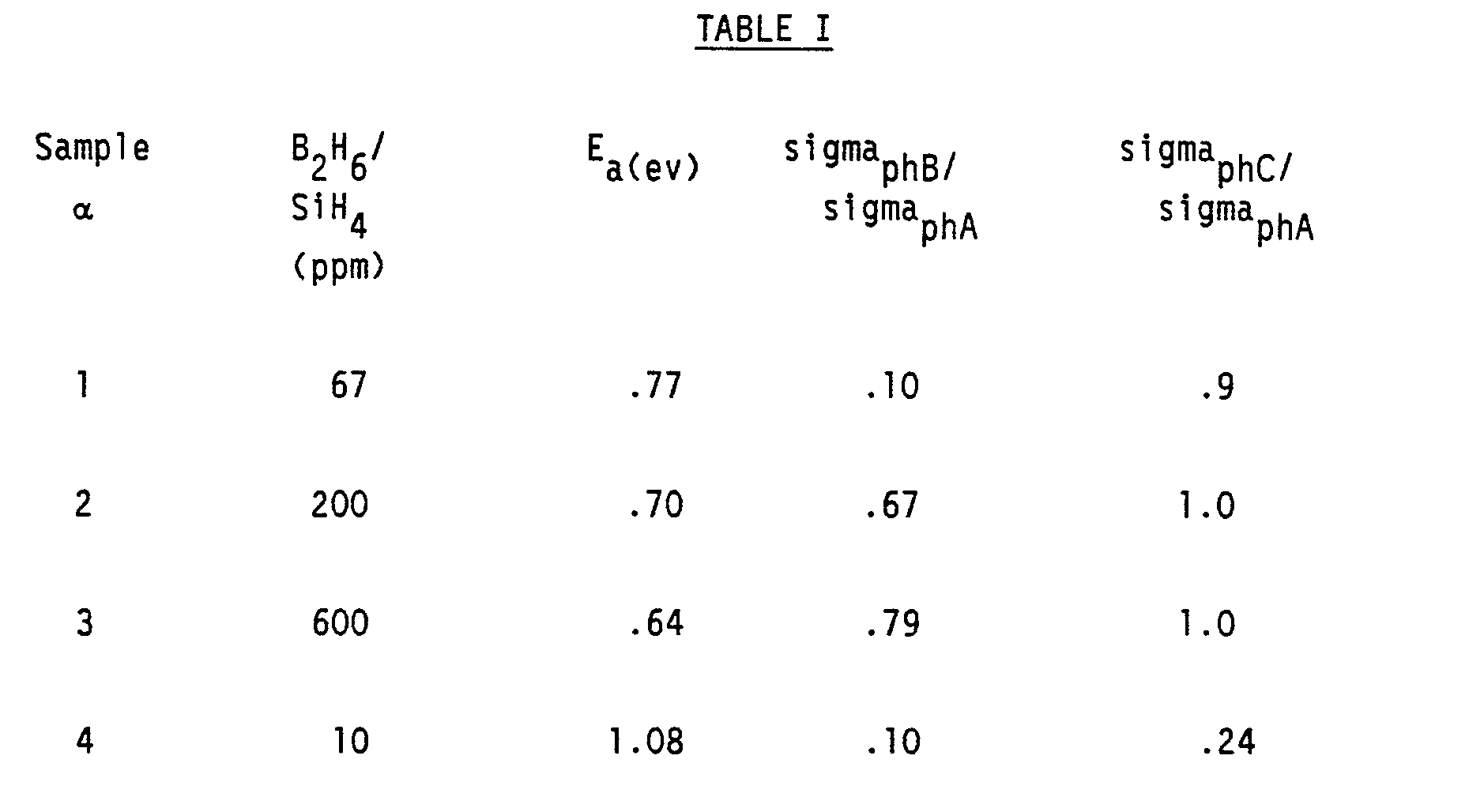
- the fourth column lists the ratio of the photoconductivity of the photo-degraded, and subsequently low-temperature annealed sample of amorphous silicon (sigma phc ) to the photoconductivity of the reference annealed sample (sigmap hA ).
- Column 3 is thus a measure of the degree of photo-degradation occuring in the sample after light soaking (exposure to illumination of AM1 intensity) and
- column 4 represents a measure of the recovery of that sample after the annealing at 100°C for 15 minutes. The larger the number in column 3, the lower the degree of photo-degradation of the sample, and the large the number in column 4, the greater the recovery of the sample after annealing.
- the photoconductivity data of Table 1 was measured parallel to the layer of silicon using colloidal graphite electrical contacts spaced approximately 2 mm apart. A constant voltage of approximately 100 volts was applied to the sample, and the flow of current was measured as a function of the intensity of illumination.
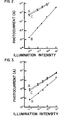
- Figure 3 is a graph of the photoconductivity data taken from sample 1 of Table 1 and illustrates the recovery of amorphous semiconductor including the low temperature annealing ingredient according to the invention.
- Line A depicts the electrical performance of sample 1 following a high temperature annealing process (2 hours at 200°C), that is, the reference performance line for the sample.
- Line B is the photoconductivity of the amorphous silicon after photo-degradation (white light illumination of 100 mW/cm 2 for 2 hours).
- Line C is the photoconductivity of the same sample following a 15 minute annealing treatment at 100°C.
- Figure 3 shows that a brief low-temperature annealing process restores the novel amorphous silicon to approximately its reference performance.
- Figure 2 is a graph similar to Figure 3 for the same sample, except that the photoconductivity was measured in a direction perpendicular to the plane of the deposited layer of amorphous silicon.
- a 50 nanometer thick layer of p +- type, i.e. heavily p doped, amorphous silicon was deposited on a chromium coated Corning 7059 glass substrate, followed by the deposition of 1.5 microns of the silicon alloy being evaluated and another 50 nanometer thick p +- type layer. Ohmic contacts were made to the chromium layer and the opposed p +- type layer.
- FIG. 3 shows that the electrical performance of the sample, as measured parallel to the layer is generally similar to the electrical performance measured through the layer shown in Figure 2.
- the overall photocurrent passed through the sample is lower in Figure 3 than in Figure 2, because of a longer the current path, but the magnitude of the changes in photocurrent on degradation and annealing is similar. Therefore, a photovoltaic device fabricated in accordance with the invention needs to be annealed only once or twice a year at a temperature of approximately 100°C for a period of time as short as 15 minutes to eliminate photo-induced defects.
- Photovoltaic devices according to the invention may be incorporated into modules specifically designed to attain and maintain elevated temperatures during operation. These annealing operations may be performed on a periodic basis, i.e., occasional hot sunny days may be relied upon to raise the semiconductor material of a photovoltaic device to the annealing temperature for a period of time sufficient to remove defects that have accumulated during the previous operation of said device. Alternatively, a continuous annealing process may be employed. In a continuous annealing process, the semiconductor material is constantly maintained at a somewhat lower annealing temperature during a significant portion of its operation.
- a module 30 includes a photovoltaic device 10 that may be similar to device 10 of Figure 1.
- a base or backing member 32 underlies photovoltaic device 10 and an encapsulant 34 forms a substantially air-tight seal between device 10 and backing member 32.
- Backing member 32 is formed from a thermally insulating material having a thermal conductivity of less than 10 -3 W/cm°C such as, for example, glass wool, styrofoam, cork, etc.
- Encapsulant 34 is preferably formed from a transparent, polymeric material such as Tedlar (registered trademark of E. I. Dupont de Nemours, Inc.) and totally encapsulates device 10 to protect it and prevent heat loss.
- photovoltaic device 10 absorbs light energy to produce electrical energy and heat. The heat cannot be conducted away because of thermal insulation provided by backing member 32 and encapsulant 34. As a result, device 10 attains and maintains an elevated temperature causing low temperature annealing.
- a module 40 includes a photovoltaic device 10 and an enclosure 42 having a bottom wall 44, four side walls, only three of which are illustrated, and a transparent cover 52.
- Enclosure 42 is either formed from, or contains, a thermal insulating material such as glass wool, styrofoam, cork, etc. and is dimensioned to receive and retain device 10 in contact with bottom wall 40.
- the side walls of enclosure 42 extend from bottom wall 40 and form an air space 54 between the front surface of device 10 and cover 52.
- Cover 52 bridges the side walls of enclosure 40 to encapsulate device 10.
- Cover 52 can be formed from glass or other similar rigid or semirigid transparent material and maybe affixed to the side walls by an adhesive, such as an epoxy adhesive.
- Incident light passes through cover 52 and strikes device 10 which absorbs the light and produces electricity and heat.
- the heat produced is prevented from escaping by backing member 32 and air space 54. In this manner, device 10 is maintained at a sufficiently elevated operating temperature to achieve low temperature annealing.
- Operating temperatures sufficient to anneal defects from a photovoltaic device according to the invention may be attained by enclosing the entire photovoltaic device in a relatively thick layer of encapsulant material having a high degree of optical transparency and relatively low thermal conductivity.
- encapsulant material having a high degree of optical transparency and relatively low thermal conductivity.
- such materials are various silicones, synthetic organic resins, inorganic glasses, and the like.
- an electrical resistance heater 60 is attached to the rear surface of a photovoltaic cell 10 to anneal the cell.
- the cell may be similar to cell 10 of Figure 1.
- An appropriate thin, sheet-like heater is a Thermofoil brand heater manufactured by Minco Products, Inc. of Minneapolis, Minnesota, U.S.A.
- a resistance heating element may be deposited directly upon the back surface of the substrate of cell 10 by screen printing or vacuum deposition.
- Electrical heater 60 includes a pair of electrical leads 62a and 62b and, preferably, a controller 64 to regulate the intensity, duration and frequency of application of heat to cell 10.
- Continuous annealing may also be achieved in a resistively heated photovoltaic device. Electrical energy may be constantly trickled to a heater so as to maintain the photovoltaic device at its annealing temperature continuously. Where ambient temperature and/or wind-chill conditions make it difficult to attain and maintain the desired annealing temperature in a passively heated module, a small resistance heater may be employed to provide sufficient additional warmth to anneal the semiconductor material.
- photoresponsive devices such as phototransistors, photodiodes, photodetectors, or any other semiconductor device, whether or not photoresponsive, that is prone to form defects in response to the absorption of photons.
Landscapes
- Photovoltaic Devices (AREA)
Abstract
Description
- Amorphous silicon alloys of electronic device quality can be prepared by glow discharge or vacuum deposition techniques. Such deposition techniques are described in U.S. Patent Nos. 4,226,898, 4,217,374, and 4,517,223 to Stanford R. Ovshinsky and others. As disclosed in those patents, fluorine introduced into the amorphous silicon semiconductor layers substantially reduces the density of the localized defect states and facilitates the addition of other alloying materials, such as germanium.
- Unlike crystalline silicon which is limited to batch processing for the manufacture of solar cells, amorphous silicon alloys can be deposited in multiple layers over large-area substrates to form solar cells in a high volume continuous processing system. Such continuous processing systems are disclosed in U.S. Patent Nos. 4,400,409, 4,410,588, 4,438,723 and 4,485,125. As disclosed in those patents, a substrate may be continuously advanced through a succession of deposition chambers, in each of which a layer of semiconductor material is deposited. In making a photovoltaic device of p-i-n configuration, the first chamber is dedicated to depositing a p-type semiconductor alloy, the second chamber is dedicated to depositing an intrinsic amorphous semiconductor alloy, and the third chamber is dedicated to depositing an n-type semiconductor alloy.
- The performance of amorphous silicon-based photovoltaic devices has been observed to degrade during operation. This process, termed "photo-degradation", or "Staebler-Wronski degradation" is believed to be caused by the breaking of weak bonds between atoms of the semiconductor material, resulting in the formation of defect states in the band gap. These photo-generated defects may be cured by annealing at elevated temperatures for a prolonged period of time, for example, a temperature of approximately 150°C for several hours.
- In an operational photovoltaic module, annealing may be carried out periodically or continuously to restore or maintain performance. A continuous annealing solar collector panel collects and retains solar thermal energy. The semiconductor material is maintained, during normal operation, at an elevated temperature (typically in excess of 100°C) and the defect states in the energy gap of the semiconductor material are annealed substantially simultaneously with their formation. However, the elevated temperatures required by the known continuous annealing process limits its use. It is therefore desirable to lower the annealing temperature.
- The problem of using a high annealing temperature is solved in the invention by including small amounts of an annealing temperature reducing agent, typically a dopant, in the charge carrier generating region of a photovoltaic device. In a typical p-i-n or n-i-p solar cell formed of amorphous silicon or amorphous silicon-germanium, the inclusion of small amounts of a dopant, such as boron, in the intrinsic semiconductor layer has been found to reduce the annealing temperature to 100°C or lower. Other dopants such as aluminum, gallium, indium, thallium and combinations of them may also be used.
- It has been reported that the addition of relatively small amounts of boron to the layer of intrinsic semiconductor material of a p-i-n photovoltaic device improves the stability of said device, but not that the dopant reduces the annealing temperature. See, "Light Induced Instability of Amorphous Silicon Photovoltaic Cells" by S. Tsuda, et al., 9 Solar Cells, 25-36 (1983) and "Stability of P-I-N Hydrogenated Amorphous Silicon Solar Cells to Light Exposure" Y. Uchida, et al., 9 Solar Cells, 3-12 (1983). The doping levels employed by Tsuda and Uchida are generally lower than those used in our invention. In contrast to our invention, any improvement in the stability or efficiency of photovoltaic devices produced in accordance with the Tsuda or Uchida publications is attributable to a change in the electric field distribution in the intrinsic region resulting from the addition of boron.
- In one embodiment of the invention, the photovoltaic device is periodically raised to its annealing temperature by an electrical heater. In another embodiment, the photovoltaic device includes a thermally insulated module that retains solar thermal energy either to raise the semiconductor material to its annealing temperature periodically or to maintain the semiconductor material at its annealing temperature constantly.
- Figure 1 is a fragmentary, cross-sectional view of a stacked photovoltaic device comprising a plurality of p-i-n type cells, each layer of the cells formed from a disordered semiconductor alloy.
- Figure 2 is a graph of photoconductivity data obtained under various conditions from a sample of semiconductor material fabricated in accordance with the invention, illustrating the improvement of the invention.
- Figure 3 is a graph of photoconductivity data obtained under various conditions from a sample of semiconductor material fabricated in accordance with the invention, illustrating the improvement of the invention.
- Figure 4 is a cross-sectional view of a photovoltaic module designed to attain and maintain an elevated temperature during at least a portion of the time of its operation and including a low temperature annealable photovoltaic material.
- Figure 5 is a cross-sectional view of an electrically heated photovoltaic module designed to attain and maintain an elevated temperature during at least a portion of the time of its operation and including a low temperature annealable photovoltaic material.
- Figure 1 shows a p-i-n type
photovoltaic device 10 made up of individualp-i-n type cells cell 12a and functions as an electrode ofcell 10. Substrate 11 may be formed of a metallic material such as thin stainless steel or aluminum, or it may be formed from a thin electroformed member such as nickel. Alternatively, substrate 11 may be formed from an insulating material such as glass or synthetic polymers, with an electrically conductive electrode layer formed on it. Although certain applications may require the deposition of a thin oxide layer and/or a series of base contacts and/or a reflecting layer upon the substrate prior to the deposition of the semiconductor material, the term, "substrate" as used here includes any such elements added by preliminary processing. - Each of the cells, 12a, 12b, and 12c are fabricated from an amorphous semiconductor body containing at least silicon or germanium. Each of the semiconductor bodies includes an n-type
conductivity semiconductor layer intrinsic semiconductor layer conductivity semiconductor layer - A TCO (transparent conductive oxide)
layer 22, formed in the preferred embodiment of indium tin oxide, is deposited on the layer of semiconductor material opposite substrate 11 and forms a second electrode. Anelectrode grid 24 may be applied toTCO layer 22 to increase current collection efficiency. - While the photovoltaic cell illlustrated in Figure 1 is a stacked assembly of p-i-n cells, the invention may also be employed with other cell arrangements such as single p-i-n cells, or stacked or single n-i-p or p-n cells.
- Applicants have shown analytically and confirmed experimentally that the incorporation of small amounts of selected annealing temperature reducing agents, such as, for example, p-dopants, into a host matrix of an intrinsic amorphous semiconductor results in a reduction in the temperature at which light-induced defects may be removed by annealing. The reduction in temperature annealing is independent of any particular device configuration in which the amorphous semiconductor may be used. Therefore, the improved amorphous semiconductor of the invention may be incorporated in a wide variety of photoresponsive devices, such as the tandem p-i-n type photovoltaic device described with reference to Figure 1.
- The improved amorphous semiconductor may be deposited by sputtering, in which case the annealing temperature reducing agent may be either present in solid form in the sputtering target, or introduced into the atmosphere in the deposition chamber in gaseous form. If introduced in an evaporation process, the annealing temperature reducing agent is either added to the solid being evaporated or added to the residual atmosphere in the deposition chamber. If chemical vapor deposition is employed for the fabrication of the amorphous semiconductor, the annealing temperature reducing agent is preferably added to the process gas stream. In an electroplating process, an appropriate amount of annealing temperature reducing agent is either added to the electrode from which the plated deposit is formed or is added directly to the plating bath. In a glow discharge process, the annealing temperature reducing agent is added to the process gas stream.
- Previously deposited layers of amorphous semiconductors may have an annealing temperature reducing agent introduced into them by ion implantation, post deposition treatment in an activated atmosphere of the annealing temperature reducing agent or a diffusion process.
- The invention is further explained with reference to the preparation of an intrinsic amorphous silicon:hydrogen alloy. This intrinsic alloy is generally similar to that utilized in intrinsic layers, 18a, 18b and 18c of
photovoltaic device 10 of Figure 1. A series of layers of an amorphous silicon:hydrogen alloy were deposited by a glow discharge process on Corning 7059 glass substrates maintained at 250°C. Silane was decomposed using radio frequency energy of 13.56 MHz. The decomposition was carried out at a pressure of approximately 27 pascal. Samples of a layer of an amorphous silicon:hydrogen alloy incorporating various levels of boron were prepared by adding differing small amounts of diborane to the chamber as the non-doped alloys were being deposited. - Each of the samples was annealed at 200°C for two hours to remove any defects created during preparation of the samples. The annealed samples were then degraded by exposure to a white light flux of approximately 100mW/cm2 for 2 hours. Photoconductivity of the degraded samples was then measured, the samples were next annealed at 100°C for 15 minutes and the photoconductivity measured again.
- The samples have a band gap of approximately 1.8 eV with the Fermi level located approximately 1.1 eV from the valence band (i.e., 0.7 eV from the conduction band), and therefore, are regarded as slightly n-type. In conventional intrinsic amorphous silicon, annealing at 100°C for 15 minutes has virtually no effect upon light-induced defects. Applicants have found that the incorporation of a p-dopant, particularly boron, in amounts sufficient to shift the Fermi level of the intrinsic amorphous semiconductor alloy toward the valence band (thereby making the intrinsic semiconductor slightly p-type) results in an improvement in the annealing characteristics. More specifically, for an amorphous silicon:hydrogen alloy that incorporates boron as the annealing temperature reducing agent, it was found that the Fermi level was shifted to a new position approximately 0.7 eV from the valence band to produce an amorphous semiconductor from which light-induced defects may be annealed by a temperature of only approximately 100°C for only approximately 15 minutes.
- Measured data appears in Table I. In the first column, the amount of diborane gas relative to the amount of silane gas present in the process gas stream is given in parts per million. The second column indicates the activation energy, in electron volts (eV), for each sample, and provides a precise basis for comparing the relative amounts of boron incorporated into the samples. Samples 1, 2 and 3 are slightly p-type, while sample 4 is very slightly n-type. The third column lists the ratio of the photoconductivity of the photo-degraded silicon semiconductor (sigmaphS) to the photoconductivity of the reference silicon alloy semiconductor (sigmaphA) which was annealed at 200°C. Finally, the fourth column lists the ratio of the photoconductivity of the photo-degraded, and subsequently low-temperature annealed sample of amorphous silicon (sigmaphc) to the photoconductivity of the reference annealed sample (sigmaphA). Column 3 is thus a measure of the degree of photo-degradation occuring in the sample after light soaking (exposure to illumination of AM1 intensity) and column 4 represents a measure of the recovery of that sample after the annealing at 100°C for 15 minutes. The larger the number in column 3, the lower the degree of photo-degradation of the sample, and the large the number in column 4, the greater the recovery of the sample after annealing.
-
- The photoconductivity data of Table 1 was measured parallel to the layer of silicon using colloidal graphite electrical contacts spaced approximately 2 mm apart. A constant voltage of approximately 100 volts was applied to the sample, and the flow of current was measured as a function of the intensity of illumination.
- The data in Table 1 show that low temperature annealing restores the slightly p-doped, photodegraded samples (samples 1, 2 and 3) to essentially their initial performance. Sample 4, which includes only very small amounts of boron and is slightly n-type, recovers only 24a of the predegradation photoconductivity following the brief, low temperature annealing process that substantially restored samples 1-3.
- Figure 3 is a graph of the photoconductivity data taken from sample 1 of Table 1 and illustrates the recovery of amorphous semiconductor including the low temperature annealing ingredient according to the invention. Line A depicts the electrical performance of sample 1 following a high temperature annealing process (2 hours at 200°C), that is, the reference performance line for the sample. Line B is the photoconductivity of the amorphous silicon after photo-degradation (white light illumination of 100 mW/cm2 for 2 hours). Line C is the photoconductivity of the same sample following a 15 minute annealing treatment at 100°C. Figure 3 shows that a brief low-temperature annealing process restores the novel amorphous silicon to approximately its reference performance.
- Figure 2 is a graph similar to Figure 3 for the same sample, except that the photoconductivity was measured in a direction perpendicular to the plane of the deposited layer of amorphous silicon. In the sample, a 50 nanometer thick layer of p+-type, i.e. heavily p doped, amorphous silicon was deposited on a chromium coated Corning 7059 glass substrate, followed by the deposition of 1.5 microns of the silicon alloy being evaluated and another 50 nanometer thick p+-type layer. Ohmic contacts were made to the chromium layer and the opposed p+-type layer. A constant voltage of approximately 0.2 volts was applied and photoconductivity measured to demonstrate that the improved annealing characteristics represent anisotropic material properties and do not depend upon any particular device configuration. Figure 3 shows that the electrical performance of the sample, as measured parallel to the layer is generally similar to the electrical performance measured through the layer shown in Figure 2. The overall photocurrent passed through the sample is lower in Figure 3 than in Figure 2, because of a longer the current path, but the magnitude of the changes in photocurrent on degradation and annealing is similar. Therefore, a photovoltaic device fabricated in accordance with the invention needs to be annealed only once or twice a year at a temperature of approximately 100°C for a period of time as short as 15 minutes to eliminate photo-induced defects.
- Photovoltaic devices according to the invention may be incorporated into modules specifically designed to attain and maintain elevated temperatures during operation. These annealing operations may be performed on a periodic basis, i.e., occasional hot sunny days may be relied upon to raise the semiconductor material of a photovoltaic device to the annealing temperature for a period of time sufficient to remove defects that have accumulated during the previous operation of said device. Alternatively, a continuous annealing process may be employed. In a continuous annealing process, the semiconductor material is constantly maintained at a somewhat lower annealing temperature during a significant portion of its operation.
- In Figure 4, a
module 30 includes aphotovoltaic device 10 that may be similar todevice 10 of Figure 1. A base or backingmember 32 underliesphotovoltaic device 10 and an encapsulant 34 forms a substantially air-tight seal betweendevice 10 andbacking member 32. Backingmember 32 is formed from a thermally insulating material having a thermal conductivity of less than 10-3 W/cm°C such as, for example, glass wool, styrofoam, cork, etc. -
Encapsulant 34 is preferably formed from a transparent, polymeric material such as Tedlar (registered trademark of E. I. Dupont de Nemours, Inc.) and totally encapsulatesdevice 10 to protect it and prevent heat loss. In operation,photovoltaic device 10 absorbs light energy to produce electrical energy and heat. The heat cannot be conducted away because of thermal insulation provided by backingmember 32 andencapsulant 34. As a result,device 10 attains and maintains an elevated temperature causing low temperature annealing. - In Figure 5 a
module 40 includes aphotovoltaic device 10 and anenclosure 42 having abottom wall 44, four side walls, only three of which are illustrated, and atransparent cover 52.Enclosure 42 is either formed from, or contains, a thermal insulating material such as glass wool, styrofoam, cork, etc. and is dimensioned to receive and retaindevice 10 in contact withbottom wall 40. The side walls ofenclosure 42 extend frombottom wall 40 and form anair space 54 between the front surface ofdevice 10 andcover 52. Cover 52 bridges the side walls ofenclosure 40 to encapsulatedevice 10.Cover 52 can be formed from glass or other similar rigid or semirigid transparent material and maybe affixed to the side walls by an adhesive, such as an epoxy adhesive. - Incident light passes through
cover 52 andstrikes device 10 which absorbs the light and produces electricity and heat. The heat produced is prevented from escaping by backingmember 32 andair space 54. In this manner,device 10 is maintained at a sufficiently elevated operating temperature to achieve low temperature annealing. - Operating temperatures sufficient to anneal defects from a photovoltaic device according to the invention may be attained by enclosing the entire photovoltaic device in a relatively thick layer of encapsulant material having a high degree of optical transparency and relatively low thermal conductivity. Among such materials are various silicones, synthetic organic resins, inorganic glasses, and the like.
- It may be desirable in some cases to use electrical heating to perform the annealing operation. In Figure 6, an
electrical resistance heater 60 is attached to the rear surface of aphotovoltaic cell 10 to anneal the cell. The cell may be similar tocell 10 of Figure 1. An appropriate thin, sheet-like heater is a Thermofoil brand heater manufactured by Minco Products, Inc. of Minneapolis, Minnesota, U.S.A. Alternatively, a resistance heating element may be deposited directly upon the back surface of the substrate ofcell 10 by screen printing or vacuum deposition.Electrical heater 60 includes a pair ofelectrical leads controller 64 to regulate the intensity, duration and frequency of application of heat tocell 10. - Continuous annealing may also be achieved in a resistively heated photovoltaic device. Electrical energy may be constantly trickled to a heater so as to maintain the photovoltaic device at its annealing temperature continuously. Where ambient temperature and/or wind-chill conditions make it difficult to attain and maintain the desired annealing temperature in a passively heated module, a small resistance heater may be employed to provide sufficient additional warmth to anneal the semiconductor material. Although the detailed discussion of the invention referred primarily to photovoltaic devices, the invention may also be applied to other types of photoresponsive devices such as phototransistors, photodiodes, photodetectors, or any other semiconductor device, whether or not photoresponsive, that is prone to form defects in response to the absorption of photons.
Claims (11)
Applications Claiming Priority (2)
| Application Number | Priority Date | Filing Date | Title |
|---|---|---|---|
| US06/637,984 US4555586A (en) | 1984-08-06 | 1984-08-06 | Photovoltiac device having long term energy conversion stability and method of producing same |
| US637984 | 1984-08-06 |
Publications (3)
| Publication Number | Publication Date |
|---|---|
| EP0171274A2 true EP0171274A2 (en) | 1986-02-12 |
| EP0171274A3 EP0171274A3 (en) | 1987-04-15 |
| EP0171274B1 EP0171274B1 (en) | 1991-01-02 |
Family
ID=24558176
Family Applications (1)
| Application Number | Title | Priority Date | Filing Date |
|---|---|---|---|
| EP85305531A Expired - Lifetime EP0171274B1 (en) | 1984-08-06 | 1985-08-02 | Photovoltaic device having long term energy conversion stability and method of producing same |
Country Status (9)
| Country | Link |
|---|---|
| US (1) | US4555586A (en) |
| EP (1) | EP0171274B1 (en) |
| JP (1) | JPS6143486A (en) |
| AU (1) | AU4566385A (en) |
| BR (1) | BR8503628A (en) |
| CA (1) | CA1226657A (en) |
| DE (1) | DE3581012D1 (en) |
| ES (1) | ES8700503A1 (en) |
| ZA (1) | ZA855545B (en) |
Cited By (1)
| Publication number | Priority date | Publication date | Assignee | Title |
|---|---|---|---|---|
| CN101924166A (en) * | 2010-08-04 | 2010-12-22 | 中国科学院光电技术研究所 | Manufacturing system and manufacturing method of solar cell surface antireflection structure |
Families Citing this family (14)
| Publication number | Priority date | Publication date | Assignee | Title |
|---|---|---|---|---|
| US4692558A (en) * | 1983-05-11 | 1987-09-08 | Chronar Corporation | Counteraction of semiconductor impurity effects |
| JPH01100975A (en) * | 1987-10-14 | 1989-04-19 | Sanyo Electric Co Ltd | Photovoltaic device |
| US7148119B1 (en) | 1994-03-10 | 2006-12-12 | Canon Kabushiki Kaisha | Process for production of semiconductor substrate |
| US20030087503A1 (en) * | 1994-03-10 | 2003-05-08 | Canon Kabushiki Kaisha | Process for production of semiconductor substrate |
| JP3315575B2 (en) * | 1996-02-07 | 2002-08-19 | キヤノン株式会社 | Solar energy conversion device, building, and temperature control method for photoelectric conversion element |
| US6806415B2 (en) * | 2000-11-10 | 2004-10-19 | Canon Kabushiki Kaisha | Method for controlling a solar power generation system having a cooling mechanism |
| KR100539639B1 (en) * | 2003-07-22 | 2005-12-29 | 전자부품연구원 | Solar cell and method of manufacturing the same |
| NZ546718A (en) * | 2006-04-19 | 2008-08-29 | Waikatolink Ltd | Energy conversion system |
| US7456042B2 (en) * | 2006-06-04 | 2008-11-25 | Robert Bosch Gmbh | Microelectromechanical systems having stored charge and methods for fabricating and using same |
| KR100905132B1 (en) | 2007-08-21 | 2009-06-29 | 강효신 | Gel lotion manufacturing method |
| EP2195856A2 (en) * | 2007-10-01 | 2010-06-16 | Suinno Oy | Thermodynamically shielded solar cell |
| US9634165B2 (en) * | 2009-11-02 | 2017-04-25 | International Business Machines Corporation | Regeneration method for restoring photovoltaic cell efficiency |
| KR20160068338A (en) * | 2014-12-05 | 2016-06-15 | 현대자동차주식회사 | A body-unity type solar cell for automobile |
| CN115207219B (en) * | 2021-04-13 | 2023-10-03 | 宁德时代新能源科技股份有限公司 | Perovskite solar cells and preparation methods and electrical equipment |
Family Cites Families (7)
| Publication number | Priority date | Publication date | Assignee | Title |
|---|---|---|---|---|
| US3597281A (en) * | 1969-05-02 | 1971-08-03 | Nasa | Recovery of radiation damaged solar cells through thermanl annealing |
| JPS5944645B2 (en) * | 1976-09-21 | 1984-10-31 | 日本電気株式会社 | solar power supply |
| US4371738A (en) * | 1981-05-04 | 1983-02-01 | Rca Corporation | Method of restoring degraded solar cells |
| JPS57187972A (en) * | 1981-05-15 | 1982-11-18 | Agency Of Ind Science & Technol | Manufacture of solar cell |
| US4409424A (en) * | 1982-06-21 | 1983-10-11 | Genevieve Devaud | Compensated amorphous silicon solar cell |
| JPS5954275A (en) * | 1982-09-22 | 1984-03-29 | Sanyo Electric Co Ltd | photovoltaic device |
| IN172491B (en) * | 1982-12-20 | 1993-09-04 | Energy Conversion Devices Inc |
-
1984
- 1984-08-06 US US06/637,984 patent/US4555586A/en not_active Expired - Lifetime
-
1985
- 1985-07-16 CA CA000486889A patent/CA1226657A/en not_active Expired
- 1985-07-23 ZA ZA855545A patent/ZA855545B/en unknown
- 1985-07-31 AU AU45663/85A patent/AU4566385A/en not_active Abandoned
- 1985-07-31 BR BR8503628A patent/BR8503628A/en unknown
- 1985-08-02 DE DE8585305531T patent/DE3581012D1/en not_active Expired - Fee Related
- 1985-08-02 EP EP85305531A patent/EP0171274B1/en not_active Expired - Lifetime
- 1985-08-05 ES ES545887A patent/ES8700503A1/en not_active Expired
- 1985-08-05 JP JP60172249A patent/JPS6143486A/en active Pending
Cited By (2)
| Publication number | Priority date | Publication date | Assignee | Title |
|---|---|---|---|---|
| CN101924166A (en) * | 2010-08-04 | 2010-12-22 | 中国科学院光电技术研究所 | Manufacturing system and manufacturing method of solar cell surface antireflection structure |
| CN101924166B (en) * | 2010-08-04 | 2013-03-06 | 中国科学院光电技术研究所 | Manufacturing system and manufacturing method of solar cell surface antireflection structure |
Also Published As
| Publication number | Publication date |
|---|---|
| JPS6143486A (en) | 1986-03-03 |
| ES8700503A1 (en) | 1986-10-01 |
| AU4566385A (en) | 1986-02-13 |
| DE3581012D1 (en) | 1991-02-07 |
| EP0171274B1 (en) | 1991-01-02 |
| US4555586A (en) | 1985-11-26 |
| EP0171274A3 (en) | 1987-04-15 |
| BR8503628A (en) | 1986-04-29 |
| ZA855545B (en) | 1986-03-26 |
| CA1226657A (en) | 1987-09-08 |
| ES545887A0 (en) | 1986-10-01 |
Similar Documents
| Publication | Publication Date | Title |
|---|---|---|
| EP0171274B1 (en) | Photovoltaic device having long term energy conversion stability and method of producing same | |
| CA1091361A (en) | Semiconductor device having an amorphous silicon active region | |
| US4459163A (en) | Amorphous semiconductor method | |
| US4536607A (en) | Photovoltaic tandem cell | |
| US4142195A (en) | Schottky barrier semiconductor device and method of making same | |
| US4117506A (en) | Amorphous silicon photovoltaic device having an insulating layer | |
| US5279679A (en) | Multi-layered photovoltaic element having at least three unit cells | |
| US8049101B2 (en) | Photovoltaic device | |
| US4398054A (en) | Compensated amorphous silicon solar cell incorporating an insulating layer | |
| JP2994812B2 (en) | Solar cell | |
| US4600801A (en) | Fluorinated, p-doped microcrystalline silicon semiconductor alloy material | |
| JP2006080557A (en) | Improved stabilization characteristics of amorphous silicon-based devices fabricated by high hydrogen dilution low temperature plasma deposition | |
| CA1226658A (en) | Fluorinated p-doped microcrystalline semiconductor alloys and method of preparation | |
| US4396793A (en) | Compensated amorphous silicon solar cell | |
| US4547621A (en) | Stable photovoltaic devices and method of producing same | |
| US4339470A (en) | Fabricating amorphous silicon solar cells by varying the temperature _of the substrate during deposition of the amorphous silicon layer | |
| JPS58500360A (en) | Amorphous semiconductor method and apparatus | |
| US4415760A (en) | Amorphous silicon solar cells incorporating an insulating layer in the body of amorphous silicon and a method of suppressing the back diffusion of holes into an N-type region | |
| JPH05110125A (en) | Photovoltaic element | |
| WO2009143136A2 (en) | System and method for high yield deposition of conductive materials onto solar cells | |
| JPH01290267A (en) | Manufacture of photoelectric conversion element | |
| CA1187588A (en) | Amorphous silicon pin semiconductor device having a hybrid construction | |
| KR101484620B1 (en) | Silicon solar cell | |
| KR810001314B1 (en) | Semiconductor Device Having Amorphous Silicon Active Region | |
| JPS59175170A (en) | Hetero junction solar battery and manufacture thereof |
Legal Events
| Date | Code | Title | Description |
|---|---|---|---|
| PUAI | Public reference made under article 153(3) epc to a published international application that has entered the european phase |
Free format text: ORIGINAL CODE: 0009012 |
|
| AK | Designated contracting states |
Designated state(s): CH DE FR GB IT LI NL |
|
| PUAL | Search report despatched |
Free format text: ORIGINAL CODE: 0009013 |
|
| AK | Designated contracting states |
Kind code of ref document: A3 Designated state(s): CH DE FR GB IT LI NL |
|
| 17P | Request for examination filed |
Effective date: 19870904 |
|
| 17Q | First examination report despatched |
Effective date: 19890621 |
|
| GRAA | (expected) grant |
Free format text: ORIGINAL CODE: 0009210 |
|
| AK | Designated contracting states |
Kind code of ref document: B1 Designated state(s): CH DE FR GB IT LI NL |
|
| ITF | It: translation for a ep patent filed | ||
| REF | Corresponds to: |
Ref document number: 3581012 Country of ref document: DE Date of ref document: 19910207 |
|
| ET | Fr: translation filed | ||
| PLBE | No opposition filed within time limit |
Free format text: ORIGINAL CODE: 0009261 |
|
| STAA | Information on the status of an ep patent application or granted ep patent |
Free format text: STATUS: NO OPPOSITION FILED WITHIN TIME LIMIT |
|
| 26N | No opposition filed | ||
| PGFP | Annual fee paid to national office [announced via postgrant information from national office to epo] |
Ref country code: NL Payment date: 19920831 Year of fee payment: 8 |
|
| PGFP | Annual fee paid to national office [announced via postgrant information from national office to epo] |
Ref country code: CH Payment date: 19920925 Year of fee payment: 8 |
|
| PG25 | Lapsed in a contracting state [announced via postgrant information from national office to epo] |
Ref country code: LI Effective date: 19930831 Ref country code: CH Effective date: 19930831 |
|
| PG25 | Lapsed in a contracting state [announced via postgrant information from national office to epo] |
Ref country code: NL Effective date: 19940301 |
|
| NLV4 | Nl: lapsed or anulled due to non-payment of the annual fee | ||
| REG | Reference to a national code |
Ref country code: CH Ref legal event code: PL |
|
| REG | Reference to a national code |
Ref country code: GB Ref legal event code: IF02 |
|
| PGFP | Annual fee paid to national office [announced via postgrant information from national office to epo] |
Ref country code: GB Payment date: 20020626 Year of fee payment: 18 |
|
| PGFP | Annual fee paid to national office [announced via postgrant information from national office to epo] |
Ref country code: FR Payment date: 20020805 Year of fee payment: 18 |
|
| PGFP | Annual fee paid to national office [announced via postgrant information from national office to epo] |
Ref country code: DE Payment date: 20020830 Year of fee payment: 18 |
|
| PG25 | Lapsed in a contracting state [announced via postgrant information from national office to epo] |
Ref country code: GB Free format text: LAPSE BECAUSE OF NON-PAYMENT OF DUE FEES Effective date: 20030802 |
|
| PG25 | Lapsed in a contracting state [announced via postgrant information from national office to epo] |
Ref country code: DE Free format text: LAPSE BECAUSE OF NON-PAYMENT OF DUE FEES Effective date: 20040302 |
|
| GBPC | Gb: european patent ceased through non-payment of renewal fee |
Effective date: 20030802 |
|
| PG25 | Lapsed in a contracting state [announced via postgrant information from national office to epo] |
Ref country code: FR Free format text: LAPSE BECAUSE OF NON-PAYMENT OF DUE FEES Effective date: 20040430 |
|
| REG | Reference to a national code |
Ref country code: FR Ref legal event code: ST |