EP0171630A2 - Système pour la production de lignes de circuit à haute résolution sur un substrat de circuit imprimé - Google Patents
Système pour la production de lignes de circuit à haute résolution sur un substrat de circuit imprimé Download PDFInfo
- Publication number
- EP0171630A2 EP0171630A2 EP85108878A EP85108878A EP0171630A2 EP 0171630 A2 EP0171630 A2 EP 0171630A2 EP 85108878 A EP85108878 A EP 85108878A EP 85108878 A EP85108878 A EP 85108878A EP 0171630 A2 EP0171630 A2 EP 0171630A2
- Authority
- EP
- European Patent Office
- Prior art keywords
- layer
- accordance
- support layer
- panel
- copper
- Prior art date
- Legal status (The legal status is an assumption and is not a legal conclusion. Google has not performed a legal analysis and makes no representation as to the accuracy of the status listed.)
- Withdrawn
Links
- RYGMFSIKBFXOCR-UHFFFAOYSA-N Copper Chemical compound [Cu] RYGMFSIKBFXOCR-UHFFFAOYSA-N 0.000 claims abstract description 63
- 229920002120 photoresistant polymer Polymers 0.000 claims abstract description 60
- 229910052802 copper Inorganic materials 0.000 claims abstract description 59
- 239000010949 copper Substances 0.000 claims abstract description 59
- 239000000758 substrate Substances 0.000 claims abstract description 42
- 238000007747 plating Methods 0.000 claims abstract description 26
- 230000001681 protective effect Effects 0.000 claims abstract description 17
- 230000005855 radiation Effects 0.000 claims abstract description 7
- 239000000126 substance Substances 0.000 claims abstract description 6
- 239000004020 conductor Substances 0.000 claims abstract description 5
- 238000000034 method Methods 0.000 claims description 41
- 239000011521 glass Substances 0.000 claims description 16
- 239000004593 Epoxy Substances 0.000 claims description 11
- 239000000463 material Substances 0.000 claims description 11
- -1 polyethylene Polymers 0.000 claims description 10
- 239000004698 Polyethylene Substances 0.000 claims description 9
- 229920000573 polyethylene Polymers 0.000 claims description 9
- 229920002799 BoPET Polymers 0.000 claims description 8
- 239000005041 Mylar™ Substances 0.000 claims description 8
- 239000002318 adhesion promoter Substances 0.000 claims description 5
- 230000007423 decrease Effects 0.000 claims description 5
- 238000010030 laminating Methods 0.000 claims description 5
- 238000004519 manufacturing process Methods 0.000 claims description 5
- 230000005611 electricity Effects 0.000 claims description 3
- 238000005530 etching Methods 0.000 claims description 3
- 230000003068 static effect Effects 0.000 claims description 3
- 230000007547 defect Effects 0.000 claims description 2
- 238000010899 nucleation Methods 0.000 claims description 2
- 206010073306 Exposure to radiation Diseases 0.000 claims 3
- 239000003989 dielectric material Substances 0.000 claims 1
- 238000007788 roughening Methods 0.000 claims 1
- ATJFFYVFTNAWJD-UHFFFAOYSA-N Tin Chemical compound [Sn] ATJFFYVFTNAWJD-UHFFFAOYSA-N 0.000 abstract description 7
- 239000011888 foil Substances 0.000 description 6
- VYZAMTAEIAYCRO-UHFFFAOYSA-N Chromium Chemical compound [Cr] VYZAMTAEIAYCRO-UHFFFAOYSA-N 0.000 description 5
- 229910052804 chromium Inorganic materials 0.000 description 5
- 239000011651 chromium Substances 0.000 description 5
- 238000007772 electroless plating Methods 0.000 description 5
- KDLHZDBZIXYQEI-UHFFFAOYSA-N Palladium Chemical compound [Pd] KDLHZDBZIXYQEI-UHFFFAOYSA-N 0.000 description 4
- QRUDEWIWKLJBPS-UHFFFAOYSA-N benzotriazole Chemical compound C1=CC=C2N[N][N]C2=C1 QRUDEWIWKLJBPS-UHFFFAOYSA-N 0.000 description 4
- 239000012964 benzotriazole Substances 0.000 description 4
- 239000011889 copper foil Substances 0.000 description 4
- 238000003475 lamination Methods 0.000 description 4
- VYPSYNLAJGMNEJ-UHFFFAOYSA-N Silicium dioxide Chemical compound O=[Si]=O VYPSYNLAJGMNEJ-UHFFFAOYSA-N 0.000 description 3
- 238000007373 indentation Methods 0.000 description 3
- 239000000243 solution Substances 0.000 description 3
- UOCLXMDMGBRAIB-UHFFFAOYSA-N 1,1,1-trichloroethane Chemical compound CC(Cl)(Cl)Cl UOCLXMDMGBRAIB-UHFFFAOYSA-N 0.000 description 2
- HCHKCACWOHOZIP-UHFFFAOYSA-N Zinc Chemical group [Zn] HCHKCACWOHOZIP-UHFFFAOYSA-N 0.000 description 2
- 239000007864 aqueous solution Substances 0.000 description 2
- 238000010586 diagram Methods 0.000 description 2
- 239000000203 mixture Substances 0.000 description 2
- 238000012986 modification Methods 0.000 description 2
- 230000004048 modification Effects 0.000 description 2
- 239000003921 oil Substances 0.000 description 2
- 229910052763 palladium Inorganic materials 0.000 description 2
- ISWSIDIOOBJBQZ-UHFFFAOYSA-N phenol group Chemical group C1(=CC=CC=C1)O ISWSIDIOOBJBQZ-UHFFFAOYSA-N 0.000 description 2
- 239000008262 pumice Substances 0.000 description 2
- 229920001169 thermoplastic Polymers 0.000 description 2
- 229920001187 thermosetting polymer Polymers 0.000 description 2
- 239000004416 thermosoftening plastic Substances 0.000 description 2
- 239000011701 zinc Substances 0.000 description 2
- 229910052725 zinc Inorganic materials 0.000 description 2
- NWONKYPBYAMBJT-UHFFFAOYSA-L zinc sulfate Chemical compound [Zn+2].[O-]S([O-])(=O)=O NWONKYPBYAMBJT-UHFFFAOYSA-L 0.000 description 2
- TXUICONDJPYNPY-UHFFFAOYSA-N (1,10,13-trimethyl-3-oxo-4,5,6,7,8,9,11,12,14,15,16,17-dodecahydrocyclopenta[a]phenanthren-17-yl) heptanoate Chemical compound C1CC2CC(=O)C=C(C)C2(C)C2C1C1CCC(OC(=O)CCCCCC)C1(C)CC2 TXUICONDJPYNPY-UHFFFAOYSA-N 0.000 description 1
- 229910021592 Copper(II) chloride Inorganic materials 0.000 description 1
- 229920000459 Nitrile rubber Polymers 0.000 description 1
- 239000004642 Polyimide Substances 0.000 description 1
- 239000004743 Polypropylene Substances 0.000 description 1
- 239000004115 Sodium Silicate Substances 0.000 description 1
- 229910021626 Tin(II) chloride Inorganic materials 0.000 description 1
- 238000000149 argon plasma sintering Methods 0.000 description 1
- QVGXLLKOCUKJST-UHFFFAOYSA-N atomic oxygen Chemical compound [O] QVGXLLKOCUKJST-UHFFFAOYSA-N 0.000 description 1
- 238000005422 blasting Methods 0.000 description 1
- 239000003054 catalyst Substances 0.000 description 1
- 239000003795 chemical substances by application Substances 0.000 description 1
- 238000004140 cleaning Methods 0.000 description 1
- 239000008139 complexing agent Substances 0.000 description 1
- ORTQZVOHEJQUHG-UHFFFAOYSA-L copper(II) chloride Chemical compound Cl[Cu]Cl ORTQZVOHEJQUHG-UHFFFAOYSA-L 0.000 description 1
- 238000005260 corrosion Methods 0.000 description 1
- 230000007797 corrosion Effects 0.000 description 1
- 230000002950 deficient Effects 0.000 description 1
- 239000008367 deionised water Substances 0.000 description 1
- 229910021641 deionized water Inorganic materials 0.000 description 1
- 230000000994 depressogenic effect Effects 0.000 description 1
- 230000001627 detrimental effect Effects 0.000 description 1
- 238000009792 diffusion process Methods 0.000 description 1
- 238000007598 dipping method Methods 0.000 description 1
- 239000000428 dust Substances 0.000 description 1
- 239000004744 fabric Substances 0.000 description 1
- 239000000945 filler Substances 0.000 description 1
- 239000003112 inhibitor Substances 0.000 description 1
- 230000000977 initiatory effect Effects 0.000 description 1
- 239000006224 matting agent Substances 0.000 description 1
- 229910052760 oxygen Inorganic materials 0.000 description 1
- 239000001301 oxygen Substances 0.000 description 1
- PIBWKRNGBLPSSY-UHFFFAOYSA-L palladium(II) chloride Chemical compound Cl[Pd]Cl PIBWKRNGBLPSSY-UHFFFAOYSA-L 0.000 description 1
- 239000002245 particle Substances 0.000 description 1
- JRKICGRDRMAZLK-UHFFFAOYSA-L peroxydisulfate Chemical compound [O-]S(=O)(=O)OOS([O-])(=O)=O JRKICGRDRMAZLK-UHFFFAOYSA-L 0.000 description 1
- 229920002492 poly(sulfone) Polymers 0.000 description 1
- 229920000515 polycarbonate Polymers 0.000 description 1
- 239000004417 polycarbonate Substances 0.000 description 1
- 229920000728 polyester Polymers 0.000 description 1
- 229920006267 polyester film Polymers 0.000 description 1
- 229920001721 polyimide Polymers 0.000 description 1
- 229920000642 polymer Polymers 0.000 description 1
- 229920000098 polyolefin Polymers 0.000 description 1
- 229920001155 polypropylene Polymers 0.000 description 1
- 150000003254 radicals Chemical class 0.000 description 1
- 239000012744 reinforcing agent Substances 0.000 description 1
- 239000011347 resin Substances 0.000 description 1
- 229920005989 resin Polymers 0.000 description 1
- 239000004576 sand Substances 0.000 description 1
- 239000000377 silicon dioxide Substances 0.000 description 1
- 235000012239 silicon dioxide Nutrition 0.000 description 1
- 239000001488 sodium phosphate Substances 0.000 description 1
- 229910000162 sodium phosphate Inorganic materials 0.000 description 1
- NTHWMYGWWRZVTN-UHFFFAOYSA-N sodium silicate Chemical compound [Na+].[Na+].[O-][Si]([O-])=O NTHWMYGWWRZVTN-UHFFFAOYSA-N 0.000 description 1
- 229910052911 sodium silicate Inorganic materials 0.000 description 1
- 239000002904 solvent Substances 0.000 description 1
- 239000001119 stannous chloride Substances 0.000 description 1
- 235000011150 stannous chloride Nutrition 0.000 description 1
- 230000008961 swelling Effects 0.000 description 1
- RYFMWSXOAZQYPI-UHFFFAOYSA-K trisodium phosphate Chemical compound [Na+].[Na+].[Na+].[O-]P([O-])([O-])=O RYFMWSXOAZQYPI-UHFFFAOYSA-K 0.000 description 1
- XLYOFNOQVPJJNP-UHFFFAOYSA-N water Chemical compound O XLYOFNOQVPJJNP-UHFFFAOYSA-N 0.000 description 1
Images


Classifications
-
- H—ELECTRICITY
- H05—ELECTRIC TECHNIQUES NOT OTHERWISE PROVIDED FOR
- H05K—PRINTED CIRCUITS; CASINGS OR CONSTRUCTIONAL DETAILS OF ELECTRIC APPARATUS; MANUFACTURE OF ASSEMBLAGES OF ELECTRICAL COMPONENTS
- H05K3/00—Apparatus or processes for manufacturing printed circuits
- H05K3/0073—Masks not provided for in groups H05K3/02 - H05K3/46, e.g. for photomechanical production of patterned surfaces
- H05K3/0082—Masks not provided for in groups H05K3/02 - H05K3/46, e.g. for photomechanical production of patterned surfaces characterised by the exposure method of radiation-sensitive masks
-
- G—PHYSICS
- G03—PHOTOGRAPHY; CINEMATOGRAPHY; ANALOGOUS TECHNIQUES USING WAVES OTHER THAN OPTICAL WAVES; ELECTROGRAPHY; HOLOGRAPHY
- G03F—PHOTOMECHANICAL PRODUCTION OF TEXTURED OR PATTERNED SURFACES, e.g. FOR PRINTING, FOR PROCESSING OF SEMICONDUCTOR DEVICES; MATERIALS THEREFOR; ORIGINALS THEREFOR; APPARATUS SPECIALLY ADAPTED THEREFOR
- G03F7/00—Photomechanical, e.g. photolithographic, production of textured or patterned surfaces, e.g. printing surfaces; Materials therefor, e.g. comprising photoresists; Apparatus specially adapted therefor
- G03F7/16—Coating processes; Apparatus therefor
- G03F7/161—Coating processes; Apparatus therefor using a previously coated surface, e.g. by stamping or by transfer lamination
-
- H—ELECTRICITY
- H05—ELECTRIC TECHNIQUES NOT OTHERWISE PROVIDED FOR
- H05K—PRINTED CIRCUITS; CASINGS OR CONSTRUCTIONAL DETAILS OF ELECTRIC APPARATUS; MANUFACTURE OF ASSEMBLAGES OF ELECTRICAL COMPONENTS
- H05K2201/00—Indexing scheme relating to printed circuits covered by H05K1/00
- H05K2201/01—Dielectrics
- H05K2201/0104—Properties and characteristics in general
- H05K2201/0108—Transparent
-
- H—ELECTRICITY
- H05—ELECTRIC TECHNIQUES NOT OTHERWISE PROVIDED FOR
- H05K—PRINTED CIRCUITS; CASINGS OR CONSTRUCTIONAL DETAILS OF ELECTRIC APPARATUS; MANUFACTURE OF ASSEMBLAGES OF ELECTRICAL COMPONENTS
- H05K2203/00—Indexing scheme relating to apparatus or processes for manufacturing printed circuits covered by H05K3/00
- H05K2203/06—Lamination
- H05K2203/066—Transfer laminating of insulating material, e.g. resist as a whole layer, not as a pattern
-
- H—ELECTRICITY
- H05—ELECTRIC TECHNIQUES NOT OTHERWISE PROVIDED FOR
- H05K—PRINTED CIRCUITS; CASINGS OR CONSTRUCTIONAL DETAILS OF ELECTRIC APPARATUS; MANUFACTURE OF ASSEMBLAGES OF ELECTRICAL COMPONENTS
- H05K2203/00—Indexing scheme relating to apparatus or processes for manufacturing printed circuits covered by H05K3/00
- H05K2203/11—Treatments characterised by their effect, e.g. heating, cooling, roughening
- H05K2203/1152—Replicating the surface structure of a sacrificial layer, e.g. for roughening
-
- H—ELECTRICITY
- H05—ELECTRIC TECHNIQUES NOT OTHERWISE PROVIDED FOR
- H05K—PRINTED CIRCUITS; CASINGS OR CONSTRUCTIONAL DETAILS OF ELECTRIC APPARATUS; MANUFACTURE OF ASSEMBLAGES OF ELECTRICAL COMPONENTS
- H05K3/00—Apparatus or processes for manufacturing printed circuits
- H05K3/10—Apparatus or processes for manufacturing printed circuits in which conductive material is applied to the insulating support in such a manner as to form the desired conductive pattern
- H05K3/108—Apparatus or processes for manufacturing printed circuits in which conductive material is applied to the insulating support in such a manner as to form the desired conductive pattern by semi-additive methods; masks therefor
Definitions
- the present invention relates to a system for producing printed circuit boards and more particularly for using a photoresist structure to produce high resolution circuit lines on said boards.
- Two common methods are currently used for producing printed circuit boards.
- One of the simplest processes consists of laminating copper foil onto a dielectric substrate, normally epoxy prepreg (pre-loaded mat or fabric); laminating a multi-layer photoresist structure, including a photoresist, onto the copper foil; exposing the circuit pattern; developing the photoresist; and, in the areas where copper lines are undesirable, removing the copper by etching.
- the photoresist is stripped, leaving the copper lines on the dielectric substrate.
- a second method of producing printed circuit boards which utilizes electroless plating of the lines has been developed.
- the peel-apart copper comprises a 50 p m copper carrier layer bonded to a thin chromium interface layer which, in turn, is bonded to a 5 um copper layer having a dendritic surface.
- the peel-apart copper is removed; the remaining copper surface is mechanically srubbed with pumice, and an adhesion promoter, benzotriazole (BTA), is applied; a photoresist structure is laminated onto the foil after the removal of the protective cover sheet layer; artwork is placed next to the photoresist and the latter is exposed through the support layer under the artwork pattern; the support layer is removed from the photoresist; and the pattern is developed.
- the board is plated, first with copper and then with tin.
- the photoresist is stripped, the undesired copper etched, and the tin removed.
- U.S. Patent No. 4,135,988 describes an alternative method for eliminating, in the plating of plated through-hole circuit boards, the problem of undercutting mentioned above. This process differs from the two methods of electroless plating previously described in that it uses a copper seeder/ catalyst rather than a palladium/tin seeder. Furthermore, the copper plating must be stripped and the board replated to improve copper-to- copper adhesion after the photoresist has been removed. An additional plating is also necessary to achieve the desired copper thickness.
- U.S. Patent No. 4,413,051 describes a method for providing high resolution, highly defined, thick film patterns. This method uses multiple layers of dry resist to achieve the desired patterns. Moreover, the polyester support sheet is peeled off of the photoresist structure and replaced on the top layer by a layer of oil. The removal of the support sheet prevents light leakage from off-axis rays and thus improves the definition of the resulting patterned resist. The oil is provided to prevent oxygen from reacting with free radicals in the photoresist sheet.
- a photohardenable element or structure having a protective cover sheet, a substantially clear support layer disposed beneath the cover sheet layer, and a photoresist layer sandwiched therebetween.
- the protective cover sheet layer is removed, and the remaining two layers of the photohardenable element are laminated onto a plating substrate to form a panel.
- Artwork is provided in contact with the support layer; the artwork and panel are exposed through the support layer to radiation; the support layer of the photohardenable element is removed; and the panel is developed. Finally, the panel is plated with an electrical conducting substance to adhere to the plating substrate to form electrical conductors and the photoresist is removed.
- the protective cover sheet layer of the photohardenable element is removed, and the remaining two layers of the photohardenable element are laminated onto a plating substrate covered with a thin layer of copper, to form a panel.
- Artwork is provided in contact with the support layer; the artwork and panel are exposed to radiation through the support layer; the support layer of the photo- hardenable element is removed; and the panel is developed.
- the panel is plated with an electrical conducting substance and then with thin.
- the photoresist is removed.
- the thin copper layer is etched in areas where printed circuit lines are not desirable and the tin is removed.
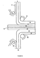
- the photoresist structure 9 has a substantially clear support layer 10, such as Mylar clear polyester film model 92D, manufactured by E.I. Du Pont de Nemours. (Mylar is a registered trademark of E.I. Du Pont de Nemours Co., Inc.).
- a photopolymer 12 a light sensitive photopolymerizable material such as model T168 Du Pont photoresist, is bonded to the support layer 10.
- a polyethylene cover sheet 14 is bonded to the photopolymer 12. As shown, the polyethylene cover sheet 14 is stripped and the remaining two layers 10, 12 are applied to a glass/epoxy substrate 16 clad with copper 18.
- thermosetting polymeric materials include epoxy, phenolic base materials, and polyimides.
- the dielectric substrates may be molded of the polymers containing fillers and/or reinforcing agents such as glass filled epoxy or phenolic base materials.
- Suitable thermoplastic polymeric materials include polyolefins such as polypropylene, polysulfones, polycarbonates and nitrile rubbers.
- the top and bottom rollers 20 and 22 provide heat and pressure during the lamination process.
- the photoresist structures 9 and 35 may be applied in the same manner to both sides of the glass/epoxy substrate 16 clad with copper 18 and 28. This provides for the production of circuit lines on both sides of the printed circuit board.
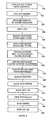
- the photoresist structures 9 and/or 35 are used in the inventive method described in FIG. 3.
- the copper sheet 18 having a roughened surface is pressure laminated onto the surface of the dielectric substrate 16, step 100.
- the copper is completely etched off, step 102, preferably by using an aqueous solution, free of complexing agents and containing CuCl 2 and HC1.
- An aqueous solution of persulfate can also be used as an agent.
- anchor points for the copper have developed at the surface to be plated. These anchor points facilitate the plating of copper afterwards and improve its adhesion to the surface.
- the cleaner is rinsed off with deionized water having a temperature of between 45°C and 60°C.
- the substrate surface 16 is activated or seeded, step 104, by contact with a composition containing palladium chloride, HC1 and stannous chloride, capable of initiating the electroless plating process.
- the seeding is performed in a one-step process.
- the substrate surface is brought into contact with the colloidal solution at room temperature for five minutes. However, the contact time can vary between 1 minute and 10 minutes.
- the polyethylene cover sheet 14 is removed, step 106.
- the remaining two layers 10, 12 of the photoresist structure 9 are then laminated onto the board 16, step 108, by heat and pressure, forming a panel.
- the rollers used in this lamination, step 108 have a temperature of approximately 100°C and exert a pressure of between 179 and 207 kPa. If printed circuit lines are to be produced on both sides 18, 28 (FIG. 2) of the board or panel 16, the photoresist structures 9, 35 are laminated on both sides of the dried substrate surface using the aforementioned temperature and pressure.
- the support layer 10 of the photoresist structure 9 should be made of a material with a haze rating or value on the Gardener haze mater of less than 2%.
- Du Pont's Mylar, model 92D is such a material, with a typical haze rating of 0.5%.
- a hazy material tends to scatter light. Instead of collimated light exposing the line channels cleanly, the scattered light exposes the photoresist in areas which are not intended to be exposed or does not expose photoresist in areas that are intended to be exposed. This leads to the hole voids and fluting of the side walls described earlier. Replacing a hazy layer with a substantially clear Mylar layer solves these problems.
- the panel is exposed to ultraviolet radiation through a glass master pattern which contains the desired circuit lines by placing the glass master, now shown, into the expose machine, aligning the glass master and then placing the panel on top of the glass master.
- the expose machine then applies a vacuum to provide a tight seal between the support sheet 10 and the glass master.
- the resist 12 is exposed through the support sheet 10 by UV light to give the proper cross link density.
- the clear support layer 10 is removed from the panel 16, step 114, and the photoresist 12 is developed, step 116, producing the negative of the desired circuit pattern on the photoresist foil 112. In the areas where the photoresist 12 has been removed in the development step 116, the catalyzed regions of the substrate surface 16 are exposed.
- the photoresist process has no detrimental effect on the catalyzed surfaces, including the through-holes.
- copper is plated by electroless plating onto the exposed surface areas, step 118.
- the plating is done in two steps which differ in the composition of the baths used and in the duration of the step.
- the photoresist is stripped, leaving the circuit lines on the board, step 120.
- peel-apart copper is laminated onto a substrate, step 124.
- the peel-apart copper comprises a 50 ⁇ m copper layer bonded to a chromium interface layer having a thickness on the order of 5-10 nm.
- the carrier layer need not be copper; any suitable material onto which a thin layer of copper may be plated or deposited can be used.
- the chromium layer is bonded to a microthin (5 ⁇ m) copper layer having a dentritic surface.
- the underside of the 5 ⁇ m copper layer is a zinc surface treated to provide a thin zincate layer.
- the 50 um copper carrier is used to protect the 5 ⁇ m copper layer from epoxy dust and small depressions during a subsequent lamination process.
- the chromium interface layer is essential for peeling the copper carrier foil from the 5 ⁇ m copper layer.
- the 5 ⁇ m copper layer is the base structure of printed circuit lines and has a dentritic surface to enhance mechanical bonding during the lamination process along with a zinc treatment.
- the zincate layer promotes adhesion between copper and epoxy.
- the basic structure is laminated by suitable heat and pressure to epoxy which may contain one or more internal copper planes that serve as signal and ground planes.
- the copper carrier and chromium interface layers are then peeled off, step 126, leaving the 5 pm copper layer 18 on the epoxy laminate 16.
- the copper surface is mechanically scrubbed with pumice to roughen the surface, step 128.
- the copper surface is then treated with a corrosion inhibitor and adhesion promoter, typically benzotriazole (BTA), by dipping the panels into a solution thereof, step 130.
- BTA benzotriazole
- the protective cover sheet layer 14 is removed from the photoresist structure 9 described above, step 132.
- the remaining two layers, 10 and 12, are laminated by heat and pressure onto one or both sides of the board, step 134.
- the circuit board is then exposed to the glass master pattern, which contains the desired circuit lines, step 135, by placing the glass master into the expose machine, aligning the glass master, and placing the panel on top of the glass master.
- the expose machine applies a vacuum, creating a tight seal between the support layer 10 of the photoresist structure and the glass master.
- the photoresist is then exposed through the support layer 10 by ultraviolet light to give the proper cross link density.
- the clear support layer 10 of the photoresist structure is removed, step 138, and the pattern is developed, step 140.
- the unexposed photoresist is developed out or chemically removed with methylchloroform.
- the exposed photoresist has been cross linked or polymerized by the ultraviolet light, becoming insoluble in the methylchloroform developer. It remains on the circuit panel during the development operation.
- the circuit panels are electrolessly plated in a copper bath, step 142, with a temperature of about 75°C and a PH of 11% to 12.
- the copper plating rate is approximately 2.0 to 2.3 um per hour. Twenty to 24 hours are required to plate up to 50 um.
- the panels are plated with tin, step 144.
- the photoresist is then removed, step 146, and the copper 18 etched from the unplated areas, step 148.
- the tin is stripped from the circuit lines, step 150.
- a problem that may arise in the use of the clear Mylar support layer 10 is indentations in the smooth surface caused by air trapped between the Mylar support sheet 10 and the polyethylene cover sheet 14 when the photo resist structure 9 is in a roll, not shown. These indentations remain for a time after the photoresist structure 9 is laminated onto the substrate 16. If the substrate 16 is plated before the indentations disappear, circuit lines will plate over the top of the depressed resist 9, resulting in variable circuit line width and possibly height. Such defective circuit lines could cause an electrical short circuit with adjacent circuit lines
- the smooth polyethylene cover sheet 14 may be matted or textured, enabling the trapped air to escape when the photoresist structure 9 is wound into a roll.
- the matting of the polyethylene layer 14 may be accomplished by imprinting a pattern on the sheet 14 or by using a matting agent such as silicon dioxide or other small mat-type particles during the manufacturing process.
- the matting of the polyethylene layer 14 also reduces static electricity when the polyethylene 14 is stripped off and the remaining layers are placed on the substrate 16.
Landscapes
- Engineering & Computer Science (AREA)
- Physics & Mathematics (AREA)
- General Physics & Mathematics (AREA)
- Manufacturing & Machinery (AREA)
- Microelectronics & Electronic Packaging (AREA)
- Parts Printed On Printed Circuit Boards (AREA)
- Manufacturing Of Printed Wiring (AREA)
Applications Claiming Priority (2)
| Application Number | Priority Date | Filing Date | Title |
|---|---|---|---|
| US63963684A | 1984-08-10 | 1984-08-10 | |
| US639636 | 1984-08-10 |
Publications (2)
| Publication Number | Publication Date |
|---|---|
| EP0171630A2 true EP0171630A2 (fr) | 1986-02-19 |
| EP0171630A3 EP0171630A3 (fr) | 1987-06-16 |
Family
ID=24564939
Family Applications (1)
| Application Number | Title | Priority Date | Filing Date |
|---|---|---|---|
| EP85108878A Withdrawn EP0171630A3 (fr) | 1984-08-10 | 1985-07-16 | Système pour la production de lignes de circuit à haute résolution sur un substrat de circuit imprimé |
Country Status (2)
| Country | Link |
|---|---|
| EP (1) | EP0171630A3 (fr) |
| JP (1) | JPS6148831A (fr) |
Cited By (5)
| Publication number | Priority date | Publication date | Assignee | Title |
|---|---|---|---|---|
| EP0298422A3 (en) * | 1987-07-08 | 1990-10-31 | Hitachi, Ltd. | Wiring method |
| EP0490118A1 (fr) * | 1990-12-10 | 1992-06-17 | Shipley Company Inc. | Masque de soudure dont l'image est obtenue par voie photographique et composition photosensible |
| US5139923A (en) * | 1987-07-08 | 1992-08-18 | Hitachi, Ltd. | Method for improving adhesion of a resist layer to a metallic layer and electrolessly plating a wiring pattern thereon |
| WO1998020395A1 (fr) * | 1996-11-08 | 1998-05-14 | W.L. Gore & Associates, Inc. | Procede pour appliquer une photoresine seche |
| WO1999015936A1 (fr) * | 1997-09-19 | 1999-04-01 | Hitachi Chemical Company, Ltd. | Element photosensible comportant un film protecteur |
Family Cites Families (2)
| Publication number | Priority date | Publication date | Assignee | Title |
|---|---|---|---|---|
| US3746541A (en) * | 1971-01-28 | 1973-07-17 | Western Electric Co | Method of irradiating a non-line-of-sight surface of a substrate |
| BE876186A (fr) * | 1979-05-11 | 1979-09-03 | Pactel Corp | Procede de fabrication de circuits imprimes tres denses |
-
1985
- 1985-06-04 JP JP11989285A patent/JPS6148831A/ja active Pending
- 1985-07-16 EP EP85108878A patent/EP0171630A3/fr not_active Withdrawn
Cited By (7)
| Publication number | Priority date | Publication date | Assignee | Title |
|---|---|---|---|---|
| EP0298422A3 (en) * | 1987-07-08 | 1990-10-31 | Hitachi, Ltd. | Wiring method |
| US5139923A (en) * | 1987-07-08 | 1992-08-18 | Hitachi, Ltd. | Method for improving adhesion of a resist layer to a metallic layer and electrolessly plating a wiring pattern thereon |
| EP0490118A1 (fr) * | 1990-12-10 | 1992-06-17 | Shipley Company Inc. | Masque de soudure dont l'image est obtenue par voie photographique et composition photosensible |
| WO1998020395A1 (fr) * | 1996-11-08 | 1998-05-14 | W.L. Gore & Associates, Inc. | Procede pour appliquer une photoresine seche |
| WO1999015936A1 (fr) * | 1997-09-19 | 1999-04-01 | Hitachi Chemical Company, Ltd. | Element photosensible comportant un film protecteur |
| US7645561B1 (en) | 1997-09-19 | 2010-01-12 | Hitachi Chemical Company, Ltd. | Photosensitive film |
| US7687224B2 (en) | 1997-09-19 | 2010-03-30 | Hitachi Chemical Company, Ltd. | Photosensitive film |
Also Published As
| Publication number | Publication date |
|---|---|
| EP0171630A3 (fr) | 1987-06-16 |
| JPS6148831A (ja) | 1986-03-10 |
Similar Documents
| Publication | Publication Date | Title |
|---|---|---|
| US6775907B1 (en) | Process for manufacturing a printed wiring board | |
| US5158860A (en) | Selective metallization process | |
| CA1131790A (fr) | Methode d'application de toner et de lavage au solvant dans la fabrication d'interconnexions conductrices | |
| US4775611A (en) | Additive printed circuit boards with flat surface and indented primary wiring conductors | |
| JP3229286B2 (ja) | プリント回路基板の製造方法 | |
| US5354593A (en) | Multilayer circuit board having microporous layers and method for making same | |
| JPS5823957B2 (ja) | 印刷回路エレメント中にメツキ孔を形成する方法 | |
| JP5483658B2 (ja) | 配線基板の製造方法 | |
| EP0171630A2 (fr) | Système pour la production de lignes de circuit à haute résolution sur un substrat de circuit imprimé | |
| JPH035078B2 (fr) | ||
| KR100343389B1 (ko) | 다층 배선기판의 제조방법 | |
| JPH08186373A (ja) | プリント配線板の製造方法 | |
| JP2689944B2 (ja) | 回路基板の製造方法 | |
| IE51721B1 (en) | Process for the manufacture of printed circuits | |
| EP0451254B1 (fr) | Carte de circuits multicouches a couches microporeuses et son procede de fabrication | |
| JP3828205B2 (ja) | 転写用部材の製造方法及び転写用部材 | |
| JPH0918154A (ja) | 回路板製造方法 | |
| JPH10190183A (ja) | メッキされた抵抗器を有するプリント回路板の製法 | |
| JP2005085898A (ja) | プリント配線基板の製造方法 | |
| JPH06252529A (ja) | プリント配線板の製造方法 | |
| JP3773567B2 (ja) | プリント配線板の製造方法 | |
| JP3761200B2 (ja) | 配線板の製造方法 | |
| JPH05283843A (ja) | 電気絶縁基板表面又は基板上の電気絶縁層表面への導体パターンの形成方法 | |
| JPH08222835A (ja) | 印刷配線板の製造方法 | |
| JPH04326587A (ja) | 印刷配線板の製造方法 |
Legal Events
| Date | Code | Title | Description |
|---|---|---|---|
| PUAI | Public reference made under article 153(3) epc to a published international application that has entered the european phase |
Free format text: ORIGINAL CODE: 0009012 |
|
| AK | Designated contracting states |
Designated state(s): DE FR GB |
|
| 17P | Request for examination filed |
Effective date: 19860624 |
|
| PUAL | Search report despatched |
Free format text: ORIGINAL CODE: 0009013 |
|
| AK | Designated contracting states |
Kind code of ref document: A3 Designated state(s): DE FR GB |
|
| 17Q | First examination report despatched |
Effective date: 19880307 |
|
| STAA | Information on the status of an ep patent application or granted ep patent |
Free format text: STATUS: THE APPLICATION IS DEEMED TO BE WITHDRAWN |
|
| 18D | Application deemed to be withdrawn |
Effective date: 19880719 |
|
| RIN1 | Information on inventor provided before grant (corrected) |
Inventor name: WELSH, JOHN A. Inventor name: CANESTARO, MICHAEL J. Inventor name: PARSONS, RALPH E. Inventor name: STEPHANIE, JOHN G. Inventor name: MESLEY, NIMROD N. |