EP0171662A2 - Procédé pour fabriquer des couches d'interposition pour chip - Google Patents
Procédé pour fabriquer des couches d'interposition pour chip Download PDFInfo
- Publication number
- EP0171662A2 EP0171662A2 EP85109180A EP85109180A EP0171662A2 EP 0171662 A2 EP0171662 A2 EP 0171662A2 EP 85109180 A EP85109180 A EP 85109180A EP 85109180 A EP85109180 A EP 85109180A EP 0171662 A2 EP0171662 A2 EP 0171662A2
- Authority
- EP
- European Patent Office
- Prior art keywords
- interposer
- etching
- support
- via holes
- single chip
- Prior art date
- Legal status (The legal status is an assumption and is not a legal conclusion. Google has not performed a legal analysis and makes no representation as to the accuracy of the status listed.)
- Granted
Links
Images



Classifications
-
- H—ELECTRICITY
- H10—SEMICONDUCTOR DEVICES; ELECTRIC SOLID-STATE DEVICES NOT OTHERWISE PROVIDED FOR
- H10W—GENERIC PACKAGES, INTERCONNECTIONS, CONNECTORS OR OTHER CONSTRUCTIONAL DETAILS OF DEVICES COVERED BY CLASS H10
- H10W70/00—Package substrates; Interposers; Redistribution layers [RDL]
- H10W70/60—Insulating or insulated package substrates; Interposers; Redistribution layers
- H10W70/62—Insulating or insulated package substrates; Interposers; Redistribution layers characterised by their interconnections
- H10W70/63—Vias, e.g. via plugs
- H10W70/635—Through-vias
-
- H—ELECTRICITY
- H10—SEMICONDUCTOR DEVICES; ELECTRIC SOLID-STATE DEVICES NOT OTHERWISE PROVIDED FOR
- H10W—GENERIC PACKAGES, INTERCONNECTIONS, CONNECTORS OR OTHER CONSTRUCTIONAL DETAILS OF DEVICES COVERED BY CLASS H10
- H10W70/00—Package substrates; Interposers; Redistribution layers [RDL]
- H10W70/01—Manufacture or treatment
- H10W70/05—Manufacture or treatment of insulating or insulated package substrates, or of interposers, or of redistribution layers
- H10W70/095—Manufacture or treatment of insulating or insulated package substrates, or of interposers, or of redistribution layers of vias therein
-
- H—ELECTRICITY
- H10—SEMICONDUCTOR DEVICES; ELECTRIC SOLID-STATE DEVICES NOT OTHERWISE PROVIDED FOR
- H10W—GENERIC PACKAGES, INTERCONNECTIONS, CONNECTORS OR OTHER CONSTRUCTIONAL DETAILS OF DEVICES COVERED BY CLASS H10
- H10W70/00—Package substrates; Interposers; Redistribution layers [RDL]
- H10W70/60—Insulating or insulated package substrates; Interposers; Redistribution layers
- H10W70/611—Insulating or insulated package substrates; Interposers; Redistribution layers for connecting multiple chips together
-
- H—ELECTRICITY
- H10—SEMICONDUCTOR DEVICES; ELECTRIC SOLID-STATE DEVICES NOT OTHERWISE PROVIDED FOR
- H10W—GENERIC PACKAGES, INTERCONNECTIONS, CONNECTORS OR OTHER CONSTRUCTIONAL DETAILS OF DEVICES COVERED BY CLASS H10
- H10W90/00—Package configurations
- H10W90/401—Package configurations characterised by multiple insulating or insulated package substrates, interposers or RDLs
-
- H—ELECTRICITY
- H05—ELECTRIC TECHNIQUES NOT OTHERWISE PROVIDED FOR
- H05K—PRINTED CIRCUITS; CASINGS OR CONSTRUCTIONAL DETAILS OF ELECTRIC APPARATUS; MANUFACTURE OF ASSEMBLAGES OF ELECTRICAL COMPONENTS
- H05K1/00—Printed circuits
- H05K1/02—Details
- H05K1/0296—Conductive pattern lay-out details not covered by sub groups H05K1/02 - H05K1/0295
- H05K1/0298—Multilayer circuits
-
- H—ELECTRICITY
- H05—ELECTRIC TECHNIQUES NOT OTHERWISE PROVIDED FOR
- H05K—PRINTED CIRCUITS; CASINGS OR CONSTRUCTIONAL DETAILS OF ELECTRIC APPARATUS; MANUFACTURE OF ASSEMBLAGES OF ELECTRICAL COMPONENTS
- H05K1/00—Printed circuits
- H05K1/02—Details
- H05K1/03—Use of materials for the substrate
- H05K1/0306—Inorganic insulating substrates, e.g. ceramic, glass
-
- H—ELECTRICITY
- H05—ELECTRIC TECHNIQUES NOT OTHERWISE PROVIDED FOR
- H05K—PRINTED CIRCUITS; CASINGS OR CONSTRUCTIONAL DETAILS OF ELECTRIC APPARATUS; MANUFACTURE OF ASSEMBLAGES OF ELECTRICAL COMPONENTS
- H05K1/00—Printed circuits
- H05K1/02—Details
- H05K1/11—Printed elements for providing electric connections to or between printed circuits
- H05K1/111—Pads for surface mounting, e.g. lay-out
- H05K1/112—Pads for surface mounting, e.g. lay-out directly combined with via connections
-
- H—ELECTRICITY
- H05—ELECTRIC TECHNIQUES NOT OTHERWISE PROVIDED FOR
- H05K—PRINTED CIRCUITS; CASINGS OR CONSTRUCTIONAL DETAILS OF ELECTRIC APPARATUS; MANUFACTURE OF ASSEMBLAGES OF ELECTRICAL COMPONENTS
- H05K1/00—Printed circuits
- H05K1/02—Details
- H05K1/11—Printed elements for providing electric connections to or between printed circuits
- H05K1/115—Via connections; Lands around holes or via connections
-
- H—ELECTRICITY
- H05—ELECTRIC TECHNIQUES NOT OTHERWISE PROVIDED FOR
- H05K—PRINTED CIRCUITS; CASINGS OR CONSTRUCTIONAL DETAILS OF ELECTRIC APPARATUS; MANUFACTURE OF ASSEMBLAGES OF ELECTRICAL COMPONENTS
- H05K3/00—Apparatus or processes for manufacturing printed circuits
- H05K3/0011—Working of insulating substrates or insulating layers
- H05K3/0017—Etching of the substrate by chemical or physical means
-
- H—ELECTRICITY
- H10—SEMICONDUCTOR DEVICES; ELECTRIC SOLID-STATE DEVICES NOT OTHERWISE PROVIDED FOR
- H10W—GENERIC PACKAGES, INTERCONNECTIONS, CONNECTORS OR OTHER CONSTRUCTIONAL DETAILS OF DEVICES COVERED BY CLASS H10
- H10W72/00—Interconnections or connectors in packages
- H10W72/071—Connecting or disconnecting
- H10W72/072—Connecting or disconnecting of bump connectors
- H10W72/07251—Connecting or disconnecting of bump connectors characterised by changes in properties of the bump connectors during connecting
-
- H—ELECTRICITY
- H10—SEMICONDUCTOR DEVICES; ELECTRIC SOLID-STATE DEVICES NOT OTHERWISE PROVIDED FOR
- H10W—GENERIC PACKAGES, INTERCONNECTIONS, CONNECTORS OR OTHER CONSTRUCTIONAL DETAILS OF DEVICES COVERED BY CLASS H10
- H10W72/00—Interconnections or connectors in packages
- H10W72/20—Bump connectors, e.g. solder bumps or copper pillars; Dummy bumps; Thermal bumps
-
- H—ELECTRICITY
- H10—SEMICONDUCTOR DEVICES; ELECTRIC SOLID-STATE DEVICES NOT OTHERWISE PROVIDED FOR
- H10W—GENERIC PACKAGES, INTERCONNECTIONS, CONNECTORS OR OTHER CONSTRUCTIONAL DETAILS OF DEVICES COVERED BY CLASS H10
- H10W90/00—Package configurations
- H10W90/701—Package configurations characterised by the relative positions of pads or connectors relative to package parts
- H10W90/721—Package configurations characterised by the relative positions of pads or connectors relative to package parts of bump connectors
- H10W90/724—Package configurations characterised by the relative positions of pads or connectors relative to package parts of bump connectors between a chip and a stacked insulating package substrate, interposer or RDL
-
- Y—GENERAL TAGGING OF NEW TECHNOLOGICAL DEVELOPMENTS; GENERAL TAGGING OF CROSS-SECTIONAL TECHNOLOGIES SPANNING OVER SEVERAL SECTIONS OF THE IPC; TECHNICAL SUBJECTS COVERED BY FORMER USPC CROSS-REFERENCE ART COLLECTIONS [XRACs] AND DIGESTS
- Y10—TECHNICAL SUBJECTS COVERED BY FORMER USPC
- Y10T—TECHNICAL SUBJECTS COVERED BY FORMER US CLASSIFICATION
- Y10T29/00—Metal working
- Y10T29/49—Method of mechanical manufacture
- Y10T29/49002—Electrical device making
- Y10T29/49117—Conductor or circuit manufacturing
- Y10T29/49124—On flat or curved insulated base, e.g., printed circuit, etc.
- Y10T29/49147—Assembling terminal to base
- Y10T29/49149—Assembling terminal to base by metal fusion bonding
-
- Y—GENERAL TAGGING OF NEW TECHNOLOGICAL DEVELOPMENTS; GENERAL TAGGING OF CROSS-SECTIONAL TECHNOLOGIES SPANNING OVER SEVERAL SECTIONS OF THE IPC; TECHNICAL SUBJECTS COVERED BY FORMER USPC CROSS-REFERENCE ART COLLECTIONS [XRACs] AND DIGESTS
- Y10—TECHNICAL SUBJECTS COVERED BY FORMER USPC
- Y10T—TECHNICAL SUBJECTS COVERED BY FORMER US CLASSIFICATION
- Y10T29/00—Metal working
- Y10T29/49—Method of mechanical manufacture
- Y10T29/49002—Electrical device making
- Y10T29/49117—Conductor or circuit manufacturing
- Y10T29/49124—On flat or curved insulated base, e.g., printed circuit, etc.
- Y10T29/49155—Manufacturing circuit on or in base
- Y10T29/49165—Manufacturing circuit on or in base by forming conductive walled aperture in base
- Y10T29/49167—Manufacturing circuit on or in base by forming conductive walled aperture in base with deforming of conductive path
Definitions
- the present invention relates to interposers for integrated circuit chips and more particularly to a method for fabncating a chip interposer, starting with a substrate featuring many chip locations, to be subsequently diced into a plurality of chip interposers, which can each carry one or more chips.
- integrated circuit chips may be mounted onto a multilayer ceramic substrate (MLC) through small solder ball joints (known as C-4 joints), which are used to bond the chips to pads on the substrate.
- MLC multilayer ceramic substrate
- C-4 joints small solder ball joints
- the MLC substrate performs a number of electrical functions: it provides voltage planes, signal lines, ground planes and redistribution planes.
- Redistribution planes are a set of planes at the top part of the module, that translate the intemal, wide, via grid of the MLC module, to the much tighter grid for the chip connections.
- the redistribution planes are the most difficult to make, since they contain a very dense via grid and very dense wiring.
- the redistribution planes are also a source of unwanted signal noise.
- TFR fine line wiring
- the fine line wiring consists of ground planes and wiring planes.
- the connection with the chips is made on top of the TFR, with the aid of terminal pads, which connect via holes at the upper surface of an MLC substrate.
- TFR depends on photolithography to make the patterns of features. TFR construction is detailed in various U.S. patents assigned to the assignee of the present invention, see for example, U.S. patents 3,726,002 and 3,968,193.
- the MLC substrate which will incorporate TFR, includes a m ⁇ lti-level metallization at a plurality of planes. Further, vertical conductive paths through the MLC layers forming the substrate are provided by a plurality of metal- filled vias.
- the TFR structure basically comprises metallurgy located at different levels separated by a plurality of insulating (e.g. polyimide or glass) layers. Vertical interconnections between different levels of metallurgy are provided through via holes.
- the first level of metal is Chromium-copper-chromium (Cr-Cu-Cr) while the second level of metal is copper-chromium (Cu-Cr).
- An additional land of metal may be formed to permit the bonding of the chip solder balls.
- Future substrates with TFR need to carry several chips.
- the size of the substrate will be in the range of approximately 6.5X6.5 cm2 to approximately 20 X 20 cm 2 , typically approximately 1 oX 10 cm 2 .
- the wiring requirements for TFR do not permit enough space for redundant lines. In other words, all lines on the TFR must be electrically sound if the substrate is to perform properly. If the substrate plus TFR are not electrically perfect, one has to either discard the (expensive) substrate or strip the TFR and begin the complex process all over again or engage in an equally expensive repair process, all of which are expensive alternatives.
- the processes required for economically making high yield, defect-free planes of fine line wiring over 1 0 X 1 0 cm 2 exceeds the capability of present and foreseen technologies.
- This technique permits one to sort out the good sections of TFR and discard the bad ones. The good sections can then be attached to the MLC substrate.
- TFR To make the TFR sections economically (i.e., to reap the benefits of batch fabrication), one has to fabricate the TFR sections on large pieces of ceramic.
- TFR is made with photolithography, which, to attain its fine line wiring capability, relies on precise location of all surface features to which it is to be aligned.
- the article entitled "Semiconductor device carrier for Modules” authored by M. T. McMahon, published in the IBM Technical Disclosure Bulletin, Vol. 18, No. 5, pp 1440 and 1441 (ref.1) is a good example of the prior art, in that it proposes an interposer made by essentially the same technology as the main body of the MLC substrate: the interposer is made by casting green sheet, punching, screening the lines and firing.
- the described interposer does not contain a ground plane, so it cannot compete with TFR-like structure.
- multichip interposers or carriers have also been suggested in the prior art; see for example IBM Technical Disclosure Bulletin, Vol. 23, No. 9, Feb. 1981, pp 4062-4063, an article entitled "Pin/chip Carrier Assembly" by S. M. Jensen et al. (ref.2).
- the multichip interposer which is described in this article is also made according to standard MLC technology. Therefore, most of the drawbacks mentioned above still remain. In particular, if any defect is found in the interposer, the whole part is to be discarded.
- a primary object of the present invention to provide a novel method of making multichip interposers including a TFR-like structure for a plurality of chips, independently of the MLC substrate, having a high manufacturing yield capability.
- a method of fabricating a multichip interposer including a TFR-like structure formed onto an insulating support (i.e., a glass ceramic sheet) which is provided with a plurality of metallized via holes associated with contact pads, permitting not only the electrical connection between the two opposite sides of the support but also its attachment to a substrate.
- the support is subsequently diced, into single chip interposers which are sorted, and only good parts are used as interposers between the chips and the MLC substrate.
- thin film fine line metallization such as a TFR-like structure is deposited onto a sheet of ceramic (glass ceramics or standard ceramics) according to a desired pattern.
- vias are then formed as follows:
- Vias and TFR are formed more easily if the TFR is formed first, then the vias are formed afterwards by the use of photolithographic techniques.
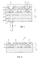
- FIG. 1 shows a partial cross sectional view of a known semiconductor device package 10 including a TFR structure 11 formed onto a MLC substrate 12 provided with contact pins 13. A semiconductor chip 14 is mounted on it. Insulating layers 15 are provided with internal metallization planes 16 which are interconnected by metal filled vias 17, for plane to plane interconnection. At the top of the MLC structure a thin film fine metallization 18 has been formed as standard, to form the "capture pad" for connecting to the MLC vias 17.
- the TFR structure is comprised of an interconnecting metallurgy 19 between insulating layers 20. Said metallurgy has been deposited in via-holes 21 formed through said insulating layers 20. The metallurgy is provided with a top surface metal layer 22 mettable by solder. The chip is joined to said metal layer 22 by standard solder ball attachment 23.
- FIG 2 shows a partial cross sectional view of a multichip interposer 24 comprised of a TFR structure 11 formed onto an insulating support 25.
- a TFR structure such as the one detailed with regards to Figure 1 (and therefore having the same numerals)
- any thin film fine line metallization such as metallurgy 18 formed a the surface of the insulating support would be appropriate as well.
- said insulating support is a blank sheet of ceramic material, including both ceramics and glass ceramics, in the range of approximately .1 mm to 3mm. In this particular application, glass ceramic,of about 1 mm thickness has been chosen.
- the invention is not limited to glass ceramics.
- Other materials could also be used, provided that they can be etched, preferably by Reactive Ion Etching (RIE) techniques or with laser assisted chemical etching.
- RIE Reactive Ion Etching
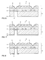
- a layer of a masking material 26 is formed onto the backside. Any material which adheres well to the ceramic substrate and does allow selective etching of the substrate may be selected, for example, chromium or aluminum.
- a thin well adhering metal layer for example, a chromium film of at least 200nm thick is evaporated on the whole backside surface.
- the chrome metal is selected because of its superior adhesion to both ceramic and glass substrates (chromium is also the bottom layer of the first level metallurgy 18 in the TFR structure).
- a layer 27 of a photoresist e.g., AZ1350J a product manufactured by A. Z. Shipley, having 1-2 microns thickness, is applied to coat the chromium layer.
- the photoresist layer is exposed through a mask (not represented) and developed. It leaves the chromium exposed in the areas 28 where the via holes or vias are to be formed.
- chromium may be etched in a Reactive Ion Etching equipment in a chlorinated plasma, such as CC1.-Argon or CC1,-N, (i.e., 50%-50%) plasma at a pressure of approximately 20 microns and a power density of approximately 1 W/cm2.
- a chlorinated plasma such as CC1.-Argon or CC1,-N, (i.e., 50%-50%) plasma at a pressure of approximately 20 microns and a power density of approximately 1 W/cm2.
- the via pattern in the chromium may be achieved by direct etching (the photoresist mask 27 is not used any longer), with an Excimer laser using chlorine, through a standard chromium on quartz projection mask.
- This etching step may be effected in a fluorinated plasma, such as CF.-O, (i.e., 90- 1 0%) plasma in a Reactive Ion Etching equipment, at a pressure of approximately 20 microns and a power density of approximately 1 W/cm 2 .
- a fluorinated plasma such as CF.-O, (i.e., 90- 1 0%) plasma in a Reactive Ion Etching equipment, at a pressure of approximately 20 microns and a power density of approximately 1 W/cm 2 .
- the RIE process finds a natural etch-stop at the surface of the bottom layer of chromium of M1 (layer 18).
- high pressure plasma etching for instance, at 1 Torr and 4 W/cm 2 in a suitable high pressure plasma reactor.
- an interconnecting metallurgy is blanket deposited over the whole back surface of the support, including the interior of via holes to form a continuous layer 30, whereby an electrical connection is made between said first level of metallization of the top side of the support and the backside.
- the preferred metal is copper because of its high conductivity. Copper is deposited by sputtering with a thickness of approximately 1 micron which permits the coating of horizontal portions and vertical portions as well. Copper reaches into the via holes and has demonstrated excellent coverage and adhesion.
- Figure 8 shows the structure after removal of excess copper and chromium using photolithographic steps. Due to the presence of relatively deep via holes, use of standard photo-resist application techniques cannot be properly used. Thus, a film of a photosensitive polymer such as Piston (a trademark of DuPont de Nemours) taped on as a mask, is recommended for this step (not represented).
- the removal of these metals can be completed either using wet processes (FeC1, for Cu and KM N O, for Cr) or by dry processes, such as laser- assisted copper and chrome etching in Cl,.
- the metal remains around each via hole as an eyelet-shaped contact pad 31 of copper with an underlying chromium ring to improve its adhesion as explained above. Oblong shaped pads may also be designed as well.
- laser induced chemical etching may be used to etch via holes 29 ( Figure 6) in the ceramic body using a reactive gas (i.e., sublimed XeF,) as an etchant gas.
- a reactive gas i.e., sublimed XeF,
- a halogen ambient may also be suitable.
- a range of operating conditions are :
- vias can be etched directly, (i.e., without using masking techniques), on the backside of the ceramic support depicted in Figure 2, by projecting the desired via pattern directly with a Nd:YAG or a CO, laser (the latter being preferred due to its higher etch rates) and reacting the material with XeF, gas. Chrome and copper are then sputter deposited, and excess metal etched away leaving metal eyelets around vias as described above.
- the resulting structure is still similar to Figure 8 except there is an underlying Cr film inside the vias as well.
- Laser processing conditions are the same as described above with their respective type of lasers. either Nd:YAG or CO,.
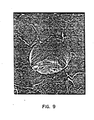
- Figure 9 is a microphotograph showing a via hole etched in a ceramic support according to said above direct laser etching techniques, which evidences the sharp definition and the smoothness of the sidewalls. There is no noticeable cratering which is usually seen in non- chemical-assisted laser etching.
- FIGS. 1 0A and 10B show respectively schematic top and bottom views of such an interposer for 4 semiconductor chips.
- the multichip interposer 24 is now tested for functionality and electrical integrity. Electrical testing by probing large areas (before dicing) is simple, since all of the chip positions are exactly in the proper locations.
- the multichip interposer is now diced into a plurality of single chip interposers referenced 24A to 24D in Figures 10A and 10B. Any known method may be used to scribe the interposer into different parts. However, a convenient manner is hereafter explained, using laser etching and plasma etching techniques for dicing.
- the individual chip carriers can be completely separated in one step after electrical testing, or alternatively, the ceramic can be partially etched prior to electrical testing, and separated into individual chip carriers after electrical testing.
- the good parts as resulting from the test operation are selected for further processing.
- An appropriate metallurgy is molybdenum-nickelgold: Mo/Ni/Au.
- Contact pads 31 on the interposer are bonded to said metallic islands 34 by brazing or using a solder 35.
- Attachment may be done either by aligning the pads and islands (such as represented in Figure 11A), or by offsetting them (such as represented in Figure 11B).
- Figure 12 shows a partial cross sectional view of a MLC substrate 12 upon which a pair of single chip interposers 24A, 24B are mounted each carrying a VLSI semiconductor chip.
- well known solder reflow techniques are employed to bond the chip solder pads to their respective chip land pattern on the interposer, such as described in U.S. patents 3,374,110 and 3,429,949 assigned to the same assignee as the present invention.
Landscapes
- Printing Elements For Providing Electric Connections Between Printed Circuits (AREA)
- Wire Bonding (AREA)
- Die Bonding (AREA)
- Production Of Multi-Layered Print Wiring Board (AREA)
Applications Claiming Priority (2)
| Application Number | Priority Date | Filing Date | Title |
|---|---|---|---|
| US639988 | 1984-08-13 | ||
| US06/639,988 US4617730A (en) | 1984-08-13 | 1984-08-13 | Method of fabricating a chip interposer |
Publications (3)
| Publication Number | Publication Date |
|---|---|
| EP0171662A2 true EP0171662A2 (fr) | 1986-02-19 |
| EP0171662A3 EP0171662A3 (en) | 1987-01-14 |
| EP0171662B1 EP0171662B1 (fr) | 1990-07-11 |
Family
ID=24566380
Family Applications (1)
| Application Number | Title | Priority Date | Filing Date |
|---|---|---|---|
| EP85109180A Expired - Lifetime EP0171662B1 (fr) | 1984-08-13 | 1985-07-23 | Procédé pour fabriquer des couches d'interposition pour chip |
Country Status (4)
| Country | Link |
|---|---|
| US (1) | US4617730A (fr) |
| EP (1) | EP0171662B1 (fr) |
| JP (1) | JPS6149443A (fr) |
| DE (1) | DE3578614D1 (fr) |
Cited By (10)
| Publication number | Priority date | Publication date | Assignee | Title |
|---|---|---|---|---|
| GB2192752A (en) * | 1986-07-16 | 1988-01-20 | Rca Corp | Semiconductor device assembly and method of making same |
| EP0260490A1 (fr) * | 1986-08-27 | 1988-03-23 | Kabushiki Kaisha Toshiba | Couche de liaison pour un composant électronique, et méthode pour lier ledit composant utilisant cette couche |
| EP0263221A1 (fr) * | 1986-10-08 | 1988-04-13 | International Business Machines Corporation | Procédé de formation de plats de brasure sur des plages de contact métalliques d'un substrat |
| EP0268111A3 (fr) * | 1986-11-17 | 1988-09-14 | International Business Machines Corporation | Procédé pour effectuer une modification technique des interconnexions entre plusieurs circuits intégrés en utilisant des pièces intermédiaires |
| US4820659A (en) * | 1986-07-16 | 1989-04-11 | General Electric Company | Method of making a semiconductor device assembly |
| WO1990003045A1 (fr) * | 1988-09-15 | 1990-03-22 | Unisys Corporation | Procede de formation de trous dans des boitiers de circuits integres en ceramique |
| EP0332559A3 (fr) * | 1988-03-11 | 1990-12-19 | International Business Machines Corporation | Procédé de fabrication d'un substrat pour supporter et connecter électriquement des composants électroniques |
| DE19632200A1 (de) * | 1996-08-09 | 1998-02-12 | Bosch Gmbh Robert | Multichipmodul |
| EP1630864A2 (fr) * | 2004-08-23 | 2006-03-01 | Tecnisco Ltd. | Substrat avec plusieurs moyens de contacts pour trou d'interconnexion |
| WO2013066504A1 (fr) * | 2011-09-14 | 2013-05-10 | Invensas Corporation | Interposeur à faible cte |
Families Citing this family (72)
| Publication number | Priority date | Publication date | Assignee | Title |
|---|---|---|---|---|
| JPS61194747A (ja) * | 1985-02-22 | 1986-08-29 | Mitsubishi Electric Corp | 樹脂封止型半導体集積回路装置 |
| US4789760A (en) * | 1985-04-30 | 1988-12-06 | Advanced Micro Devices, Inc. | Via in a planarized dielectric and process for producing same |
| EP0229850B1 (fr) * | 1985-07-16 | 1992-06-10 | Nippon Telegraph and Telephone Corporation | Bornes de connection entre des substrats et procede de production |
| US4925524A (en) * | 1987-06-12 | 1990-05-15 | Hewlett-Packard Company | Method for forming tungsten structures in a semiconductor |
| US6288561B1 (en) * | 1988-05-16 | 2001-09-11 | Elm Technology Corporation | Method and apparatus for probing, testing, burn-in, repairing and programming of integrated circuits in a closed environment using a single apparatus |
| US4924589A (en) * | 1988-05-16 | 1990-05-15 | Leedy Glenn J | Method of making and testing an integrated circuit |
| US5020219A (en) * | 1988-05-16 | 1991-06-04 | Leedy Glenn J | Method of making a flexible tester surface for testing integrated circuits |
| US5512397A (en) * | 1988-05-16 | 1996-04-30 | Leedy; Glenn J. | Stepper scanner discretionary lithography and common mask discretionary lithography for integrated circuits |
| US5225771A (en) * | 1988-05-16 | 1993-07-06 | Dri Technology Corp. | Making and testing an integrated circuit using high density probe points |
| CA2002213C (fr) * | 1988-11-10 | 1999-03-30 | Iwona Turlik | Boitier de puce de circuits integres a haute performance et sa methode de fabrication |
| US4914813A (en) * | 1988-11-25 | 1990-04-10 | Innovative Packing Technology | Refurbishing of prior used laminated ceramic packages |
| US5055907A (en) * | 1989-01-25 | 1991-10-08 | Mosaic, Inc. | Extended integration semiconductor structure with wiring layers |
| US5192716A (en) * | 1989-01-25 | 1993-03-09 | Polylithics, Inc. | Method of making a extended integration semiconductor structure |
| US4940181A (en) * | 1989-04-06 | 1990-07-10 | Motorola, Inc. | Pad grid array for receiving a solder bumped chip carrier |
| US5121299A (en) * | 1989-12-29 | 1992-06-09 | International Business Machines Corporation | Multi-level circuit structure utilizing conductive cores having conductive protrusions and cavities therein |
| JPH045844A (ja) * | 1990-04-23 | 1992-01-09 | Nippon Mektron Ltd | Ic搭載用多層回路基板及びその製造法 |
| KR930011462B1 (ko) * | 1990-11-23 | 1993-12-08 | 현대전자산업 주식회사 | 다층배선의 단차를 완화시키는 방법 |
| US5172303A (en) * | 1990-11-23 | 1992-12-15 | Motorola, Inc. | Electronic component assembly |
| US5166097A (en) * | 1990-11-26 | 1992-11-24 | The Boeing Company | Silicon wafers containing conductive feedthroughs |
| US5146674A (en) * | 1991-07-01 | 1992-09-15 | International Business Machines Corporation | Manufacturing process of a high density substrate design |
| US5279711A (en) * | 1991-07-01 | 1994-01-18 | International Business Machines Corporation | Chip attach and sealing method |
| JP2765673B2 (ja) * | 1992-06-04 | 1998-06-18 | インターナショナル・ビジネス・マシーンズ・コーポレイション | メタライゼーション層及びその形成方法 |
| US5264729A (en) * | 1992-07-29 | 1993-11-23 | Lsi Logic Corporation | Semiconductor package having programmable interconnect |
| US5512710A (en) * | 1992-08-21 | 1996-04-30 | Cts Corporation | Multilayer package with second layer via test connections |
| US5386627A (en) * | 1992-09-29 | 1995-02-07 | International Business Machines Corporation | Method of fabricating a multi-layer integrated circuit chip interposer |
| US5406701A (en) * | 1992-10-02 | 1995-04-18 | Irvine Sensors Corporation | Fabrication of dense parallel solder bump connections |
| US5329423A (en) * | 1993-04-13 | 1994-07-12 | Scholz Kenneth D | Compressive bump-and-socket interconnection scheme for integrated circuits |
| JPH08510358A (ja) * | 1993-04-14 | 1996-10-29 | アムコール・エレクトロニクス・インク | 集積回路チップと基板との相互接続 |
| US5462636A (en) * | 1993-12-28 | 1995-10-31 | International Business Machines Corporation | Method for chemically scribing wafers |
| US5861663A (en) * | 1994-12-27 | 1999-01-19 | International Business Machines Corporation | Column grid array or ball grid array pad on via |
| WO2004100260A1 (fr) * | 1995-05-19 | 2004-11-18 | Kouta Noda | Carte a circuits imprimes multicouches haute densite, support multi-puces et boitier a semi-conducteurs |
| JPH0945805A (ja) * | 1995-07-31 | 1997-02-14 | Fujitsu Ltd | 配線基板、半導体装置及び半導体装置を配線基板から取り外す方法並びに半導体装置の製造方法 |
| US6405431B1 (en) | 1996-06-27 | 2002-06-18 | Samsung Electro-Mechanics Co., Ltd. | Method for manufacturing build-up multi-layer printed circuit board by using yag laser |
| CA2232523C (fr) * | 1996-07-22 | 2004-07-13 | Honda Giken Kogyo Kabushiki Kaisha | Unite de commande electronique de type enfichable, structure de connexion entre un tableau de connexion et des fiches, unite de connexion entre des pieces electroniques et un tableau de connexion et procede de montage de pieces electroniques |
| JP4234205B2 (ja) * | 1996-11-08 | 2009-03-04 | ダブリュ.エル.ゴア アンド アソシエイツ,インコーポレイティド | 電子アセンブリおよび電子物品内でのヴァイアのインダクタンスを低減する方法 |
| US5795818A (en) * | 1996-12-06 | 1998-08-18 | Amkor Technology, Inc. | Integrated circuit chip to substrate interconnection and method |
| US5973391A (en) * | 1997-12-11 | 1999-10-26 | Read-Rite Corporation | Interposer with embedded circuitry and method for using the same to package microelectronic units |
| JPH11187542A (ja) * | 1997-12-18 | 1999-07-09 | Furukawa Electric Co Ltd:The | バスバー配線板の製造方法 |
| US6833613B1 (en) * | 1997-12-18 | 2004-12-21 | Micron Technology, Inc. | Stacked semiconductor package having laser machined contacts |
| US6620731B1 (en) * | 1997-12-18 | 2003-09-16 | Micron Technology, Inc. | Method for fabricating semiconductor components and interconnects with contacts on opposing sides |
| US6023029A (en) * | 1998-03-19 | 2000-02-08 | International Business Machines Corporation | Use of blind vias for soldered interconnections between substrates and printed wiring boards |
| US6242935B1 (en) * | 1999-01-21 | 2001-06-05 | Micron Technology, Inc. | Interconnect for testing semiconductor components and method of fabrication |
| US6319829B1 (en) | 1999-08-18 | 2001-11-20 | International Business Machines Corporation | Enhanced interconnection to ceramic substrates |
| US6392301B1 (en) * | 1999-10-22 | 2002-05-21 | Intel Corporation | Chip package and method |
| US6392428B1 (en) * | 1999-11-16 | 2002-05-21 | Eaglestone Partners I, Llc | Wafer level interposer |
| JP2001168125A (ja) * | 1999-12-03 | 2001-06-22 | Nec Corp | 半導体装置 |
| US6627998B1 (en) * | 2000-07-27 | 2003-09-30 | International Business Machines Corporation | Wafer scale thin film package |
| US6812048B1 (en) | 2000-07-31 | 2004-11-02 | Eaglestone Partners I, Llc | Method for manufacturing a wafer-interposer assembly |
| US6537831B1 (en) * | 2000-07-31 | 2003-03-25 | Eaglestone Partners I, Llc | Method for selecting components for a matched set using a multi wafer interposer |
| US6531763B1 (en) | 2000-08-15 | 2003-03-11 | Micron Technology, Inc. | Interposers having encapsulant fill control features |
| US6815712B1 (en) | 2000-10-02 | 2004-11-09 | Eaglestone Partners I, Llc | Method for selecting components for a matched set from a wafer-interposer assembly |
| US6686657B1 (en) | 2000-11-07 | 2004-02-03 | Eaglestone Partners I, Llc | Interposer for improved handling of semiconductor wafers and method of use of same |
| US6529022B2 (en) | 2000-12-15 | 2003-03-04 | Eaglestone Pareners I, Llc | Wafer testing interposer for a conventional package |
| US20020078401A1 (en) * | 2000-12-15 | 2002-06-20 | Fry Michael Andrew | Test coverage analysis system |
| US20020076854A1 (en) * | 2000-12-15 | 2002-06-20 | Pierce John L. | System, method and apparatus for constructing a semiconductor wafer-interposer using B-Stage laminates |
| US6524885B2 (en) * | 2000-12-15 | 2003-02-25 | Eaglestone Partners I, Llc | Method, apparatus and system for building an interposer onto a semiconductor wafer using laser techniques |
| US6673653B2 (en) * | 2001-02-23 | 2004-01-06 | Eaglestone Partners I, Llc | Wafer-interposer using a ceramic substrate |
| US6787916B2 (en) * | 2001-09-13 | 2004-09-07 | Tru-Si Technologies, Inc. | Structures having a substrate with a cavity and having an integrated circuit bonded to a contact pad located in the cavity |
| DE10205544A1 (de) * | 2002-02-11 | 2003-05-15 | Infineon Technologies Ag | Verfahren zur Herstellung eines elektronischen Halbleiterbauteils mit dreidimensionaler Umverdrahtungsstruktur sowie elektronisches Halbleiterbauteil |
| US6960837B2 (en) * | 2002-02-26 | 2005-11-01 | International Business Machines Corporation | Method of connecting core I/O pins to backside chip I/O pads |
| US6839965B2 (en) * | 2003-02-06 | 2005-01-11 | R-Tec Corporation | Method of manufacturing a resistor connector |
| TW566796U (en) * | 2003-03-12 | 2003-12-11 | Unimicron Technology Corp | Standard printed circuit board core |
| US7289336B2 (en) * | 2004-10-28 | 2007-10-30 | General Electric Company | Electronic packaging and method of making the same |
| US7781741B2 (en) * | 2005-10-27 | 2010-08-24 | General Electric Company | Methods and systems for controlling data acquisition system noise |
| JP5117698B2 (ja) * | 2006-09-27 | 2013-01-16 | ルネサスエレクトロニクス株式会社 | 半導体装置 |
| US8212331B1 (en) * | 2006-10-02 | 2012-07-03 | Newport Fab, Llc | Method for fabricating a backside through-wafer via in a processed wafer and related structure |
| US8080446B2 (en) * | 2009-05-27 | 2011-12-20 | Stats Chippac Ltd. | Integrated circuit packaging system with interposer interconnections and method of manufacture thereof |
| JP2012069739A (ja) * | 2010-09-24 | 2012-04-05 | Shinko Electric Ind Co Ltd | 配線基板の製造方法 |
| US9093506B2 (en) * | 2012-05-08 | 2015-07-28 | Skyworks Solutions, Inc. | Process for fabricating gallium arsenide devices with copper contact layer |
| JP6424610B2 (ja) * | 2014-04-23 | 2018-11-21 | ソニー株式会社 | 半導体装置、および製造方法 |
| WO2016143288A1 (fr) * | 2015-03-12 | 2016-09-15 | Sony Corporation | Dispositif d'imagerie, procédé de fabrication et dispositif électronique |
| US10468363B2 (en) * | 2015-08-10 | 2019-11-05 | X-Celeprint Limited | Chiplets with connection posts |
Family Cites Families (14)
| Publication number | Priority date | Publication date | Assignee | Title |
|---|---|---|---|---|
| SE377229B (fr) * | 1971-08-27 | 1975-06-23 | Ibm | |
| JPS5233787B2 (fr) * | 1972-05-10 | 1977-08-30 | ||
| JPS505377A (fr) * | 1973-05-29 | 1975-01-21 | ||
| GB1485569A (en) * | 1974-09-10 | 1977-09-14 | Siemens Ag | Multi-layer wired substrates for multi-chip circuits |
| US4074342A (en) * | 1974-12-20 | 1978-02-14 | International Business Machines Corporation | Electrical package for lsi devices and assembly process therefor |
| US4202007A (en) * | 1978-06-23 | 1980-05-06 | International Business Machines Corporation | Multi-layer dielectric planar structure having an internal conductor pattern characterized with opposite terminations disposed at a common edge surface of the layers |
| US4277321A (en) * | 1979-04-23 | 1981-07-07 | Bell Telephone Laboratories, Incorporated | Treating multilayer printed wiring boards |
| US4349862A (en) * | 1980-08-11 | 1982-09-14 | International Business Machines Corporation | Capacitive chip carrier and multilayer ceramic capacitors |
| US4386116A (en) * | 1981-12-24 | 1983-05-31 | International Business Machines Corporation | Process for making multilayer integrated circuit substrate |
| JPS5987893A (ja) * | 1982-11-12 | 1984-05-21 | 株式会社日立製作所 | 配線基板とその製造方法およびそれを用いた半導体装置 |
| GB2136203B (en) * | 1983-03-02 | 1986-10-15 | Standard Telephones Cables Ltd | Through-wafer integrated circuit connections |
| US4439270A (en) * | 1983-08-08 | 1984-03-27 | International Business Machines Corporation | Process for the controlled etching of tapered vias in borosilicate glass dielectrics |
| US4495220A (en) * | 1983-10-07 | 1985-01-22 | Trw Inc. | Polyimide inter-metal dielectric process |
| US4517050A (en) * | 1983-12-05 | 1985-05-14 | E. I. Du Pont De Nemours And Company | Process for forming conductive through-holes through a dielectric layer |
-
1984
- 1984-08-13 US US06/639,988 patent/US4617730A/en not_active Expired - Fee Related
-
1985
- 1985-07-13 JP JP60153406A patent/JPS6149443A/ja active Granted
- 1985-07-23 DE DE8585109180T patent/DE3578614D1/de not_active Expired - Lifetime
- 1985-07-23 EP EP85109180A patent/EP0171662B1/fr not_active Expired - Lifetime
Cited By (17)
| Publication number | Priority date | Publication date | Assignee | Title |
|---|---|---|---|---|
| GB2192752A (en) * | 1986-07-16 | 1988-01-20 | Rca Corp | Semiconductor device assembly and method of making same |
| US4820659A (en) * | 1986-07-16 | 1989-04-11 | General Electric Company | Method of making a semiconductor device assembly |
| GB2192752B (en) * | 1986-07-16 | 1990-01-04 | Rca Corp | Semiconductor device assembly and method of making same |
| EP0260490A1 (fr) * | 1986-08-27 | 1988-03-23 | Kabushiki Kaisha Toshiba | Couche de liaison pour un composant électronique, et méthode pour lier ledit composant utilisant cette couche |
| US4887760A (en) * | 1986-08-27 | 1989-12-19 | Kabushiki Kaisha Toshiba | Bonding sheet for electronic component and method of bonding electronic component using the same |
| EP0263221A1 (fr) * | 1986-10-08 | 1988-04-13 | International Business Machines Corporation | Procédé de formation de plats de brasure sur des plages de contact métalliques d'un substrat |
| EP0268111A3 (fr) * | 1986-11-17 | 1988-09-14 | International Business Machines Corporation | Procédé pour effectuer une modification technique des interconnexions entre plusieurs circuits intégrés en utilisant des pièces intermédiaires |
| EP0332559A3 (fr) * | 1988-03-11 | 1990-12-19 | International Business Machines Corporation | Procédé de fabrication d'un substrat pour supporter et connecter électriquement des composants électroniques |
| WO1990003045A1 (fr) * | 1988-09-15 | 1990-03-22 | Unisys Corporation | Procede de formation de trous dans des boitiers de circuits integres en ceramique |
| DE19632200A1 (de) * | 1996-08-09 | 1998-02-12 | Bosch Gmbh Robert | Multichipmodul |
| US5953213A (en) * | 1996-08-09 | 1999-09-14 | Robert Bosch Gmbh | Multichip module |
| DE19632200C2 (de) * | 1996-08-09 | 2002-09-05 | Bosch Gmbh Robert | Multichipmodul |
| EP1630864A2 (fr) * | 2004-08-23 | 2006-03-01 | Tecnisco Ltd. | Substrat avec plusieurs moyens de contacts pour trou d'interconnexion |
| WO2013066504A1 (fr) * | 2011-09-14 | 2013-05-10 | Invensas Corporation | Interposeur à faible cte |
| US8780576B2 (en) | 2011-09-14 | 2014-07-15 | Invensas Corporation | Low CTE interposer |
| US9401288B2 (en) | 2011-09-14 | 2016-07-26 | Invensas Corporation | Low CTE interposer |
| US10319673B2 (en) | 2011-09-14 | 2019-06-11 | Invensas Corporation | Low CTE interposer |
Also Published As
| Publication number | Publication date |
|---|---|
| DE3578614D1 (de) | 1990-08-16 |
| US4617730A (en) | 1986-10-21 |
| JPH0517708B2 (fr) | 1993-03-09 |
| EP0171662A3 (en) | 1987-01-14 |
| EP0171662B1 (fr) | 1990-07-11 |
| JPS6149443A (ja) | 1986-03-11 |
Similar Documents
| Publication | Publication Date | Title |
|---|---|---|
| EP0171662B1 (fr) | Procédé pour fabriquer des couches d'interposition pour chip | |
| US5244833A (en) | Method for manufacturing an integrated circuit chip bump electrode using a polymer layer and a photoresist layer | |
| US5401689A (en) | Method for forming a semiconductor chip carrier | |
| US4446477A (en) | Multichip thin film module | |
| US5010389A (en) | Integrated circuit substrate with contacts thereon for a packaging structure | |
| KR960013632B1 (ko) | 다중칩 집적회로 패키징 구성 및 방법 | |
| US6753208B1 (en) | Wafer scale method of packaging integrated circuit die | |
| US5946555A (en) | Wafer level decal for minimal packaging of chips | |
| US5386627A (en) | Method of fabricating a multi-layer integrated circuit chip interposer | |
| US4221047A (en) | Multilayered glass-ceramic substrate for mounting of semiconductor device | |
| US6621164B2 (en) | Chip size package having concave pattern in the bump pad area of redistribution patterns and method for manufacturing the same | |
| JP3285796B2 (ja) | 導電性接触パツド接続方法 | |
| US6521530B2 (en) | Composite interposer and method for producing a composite interposer | |
| US5353195A (en) | Integral power and ground structure for multi-chip modules | |
| US5485038A (en) | Microelectronic circuit substrate structure including photoimageable epoxy dielectric layers | |
| US5817541A (en) | Methods of fabricating an HDMI decal chip scale package | |
| US7338891B2 (en) | Semiconductor chip, mounting structure thereof, and methods for forming a semiconductor chip and printed circuit board for the mounting structure thereof | |
| US6636313B2 (en) | Method of measuring photoresist and bump misalignment | |
| US5108541A (en) | Processes for electrically conductive decals filled with inorganic insulator material | |
| US6297164B1 (en) | Method for producing contact structures | |
| US5198385A (en) | Photolithographic formation of die-to-package airbridge in a semiconductor device | |
| US5358826A (en) | Method of fabricating metallized chip carries from wafer-shaped substrates | |
| JPH04313247A (ja) | 同一平面の接触バンプを有する相互接続装置及びその製造方法 | |
| US6841877B2 (en) | Semiconductor device, metal laminated plate for fabricating circuit on semiconductor, and method of fabricating circuit | |
| US20050048696A1 (en) | Microbeam assembly and associated method for integrated circuit interconnection to substrates |
Legal Events
| Date | Code | Title | Description |
|---|---|---|---|
| PUAI | Public reference made under article 153(3) epc to a published international application that has entered the european phase |
Free format text: ORIGINAL CODE: 0009012 |
|
| AK | Designated contracting states |
Designated state(s): DE FR GB |
|
| 17P | Request for examination filed |
Effective date: 19860624 |
|
| PUAL | Search report despatched |
Free format text: ORIGINAL CODE: 0009013 |
|
| AK | Designated contracting states |
Kind code of ref document: A3 Designated state(s): DE FR GB |
|
| 17Q | First examination report despatched |
Effective date: 19880719 |
|
| GRAA | (expected) grant |
Free format text: ORIGINAL CODE: 0009210 |
|
| AK | Designated contracting states |
Kind code of ref document: B1 Designated state(s): DE FR GB |
|
| REF | Corresponds to: |
Ref document number: 3578614 Country of ref document: DE Date of ref document: 19900816 |
|
| ET | Fr: translation filed | ||
| PLBE | No opposition filed within time limit |
Free format text: ORIGINAL CODE: 0009261 |
|
| STAA | Information on the status of an ep patent application or granted ep patent |
Free format text: STATUS: NO OPPOSITION FILED WITHIN TIME LIMIT |
|
| 26N | No opposition filed | ||
| PGFP | Annual fee paid to national office [announced via postgrant information from national office to epo] |
Ref country code: GB Payment date: 19950622 Year of fee payment: 11 |
|
| PGFP | Annual fee paid to national office [announced via postgrant information from national office to epo] |
Ref country code: FR Payment date: 19950704 Year of fee payment: 11 |
|
| PGFP | Annual fee paid to national office [announced via postgrant information from national office to epo] |
Ref country code: DE Payment date: 19950720 Year of fee payment: 11 |
|
| PG25 | Lapsed in a contracting state [announced via postgrant information from national office to epo] |
Ref country code: GB Effective date: 19960723 |
|
| GBPC | Gb: european patent ceased through non-payment of renewal fee |
Effective date: 19960723 |
|
| PG25 | Lapsed in a contracting state [announced via postgrant information from national office to epo] |
Ref country code: FR Effective date: 19970328 |
|
| PG25 | Lapsed in a contracting state [announced via postgrant information from national office to epo] |
Ref country code: DE Effective date: 19970402 |
|
| REG | Reference to a national code |
Ref country code: FR Ref legal event code: ST |