EP0171668A1 - Elektroerosionselektrode - Google Patents
Elektroerosionselektrode Download PDFInfo
- Publication number
- EP0171668A1 EP0171668A1 EP85109250A EP85109250A EP0171668A1 EP 0171668 A1 EP0171668 A1 EP 0171668A1 EP 85109250 A EP85109250 A EP 85109250A EP 85109250 A EP85109250 A EP 85109250A EP 0171668 A1 EP0171668 A1 EP 0171668A1
- Authority
- EP
- European Patent Office
- Prior art keywords
- electrode
- silicon
- metal
- machining
- melting point
- Prior art date
- Legal status (The legal status is an assumption and is not a legal conclusion. Google has not performed a legal analysis and makes no representation as to the accuracy of the status listed.)
- Granted
Links
Images


Classifications
-
- B—PERFORMING OPERATIONS; TRANSPORTING
- B23—MACHINE TOOLS; METAL-WORKING NOT OTHERWISE PROVIDED FOR
- B23H—WORKING OF METAL BY THE ACTION OF A HIGH CONCENTRATION OF ELECTRIC CURRENT ON A WORKPIECE USING AN ELECTRODE WHICH TAKES THE PLACE OF A TOOL; SUCH WORKING COMBINED WITH OTHER FORMS OF WORKING OF METAL
- B23H1/00—Electrical discharge machining, i.e. removing metal with a series of rapidly recurring electrical discharges between an electrode and a workpiece in the presence of a fluid dielectric
- B23H1/04—Electrodes specially adapted therefor or their manufacture
- B23H1/06—Electrode material
Definitions
- the present invention relates to a electrode intended for use with an electric discharge machining apparatus. More specifically, the present invention relates to such an electrode which provides a reduced surface roughness and is well adapted for precision machining operations.
- Another object of the invention is to provide an electrode suitable for rapid finish-machining.
- the present invention provides an electrode for precision discharge machining, comprising or formed by silicon or other materials which have similar electrical or physical characteristics to those of silicon.
- the present invention provides an electrode suitable for precision electric discharge machining formed by dissolving or finely mixing a substance having high electrical resistance with silicon or other materials like silicon or a metal having a low melting point covering a body of the metal with the resulting composition.
- a substance having a high electrical resistance inorganic compounds such as semiconductors, carbides, oxides and salts of the metal can be employed.
- the metal zinc and alloys thereof are preferred.
- the electric discharge machining apparatus includes a table 1 on which is positioned a workpiece to be machined, an electrode 2 disposed opposite the workpiece, replacement electrodes 2A through 2D used for varying machining operations, a hydraulic cylinder 3 for controlling the position of the electrode 2 relative to the workpiece, a numeric controller 4 for controlling operations of the various elements of the apparatus of Fig.
- an X-axis motor 5 for moving the table 1 in the direction of the X-axis
- a Y-axis motor 6 for moving the table 1 in the direction of the Y-axis
- a power supply 7 for supplying discharge energy between the electrode 2 and the workpiece
- an electrode exchanging apparatus 8 for automatically exchanging the various electrodes 2 and 2A through 2D for the different stages of machining, namely, rough, intermediate and finish machining.
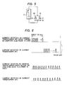
- waveforms are shown of the current supplied from the power supply 7 and the actual current flowing between the electrode 2 and the workpice 9 in the case where the parasitic capacitor 10 is charged.
- the peak value of the current applied between the electrode 2 and the workpiece 9 is much higher (in the case where the parasitic capacitor 10 is charged) than the peak value of the current supplied from the power supply .7. This is an additional reason for unwanted surface roughening of the workpiece 9.
- the electrode is divided into two segments 2 and 2'.
- Current is supplied to the segments 2 and 2' via respective current transformers 15 and 15'. If the discharge first starts between the electrode segment 2 and the workpiece 9, after machining for, for example, ten minutes, due to consumption of the electrode 2, the discharge will shift to the segment 2'. Then, discharge continues between the electrode segment 2' and the workpiece 9 until the electrode segment 2' has been consumed more than the electrode segment 2, at which time the discharge shifts back to between the electrode segment 2 and the workpiece 9. This switching back and forth of the discharge makes it difficult to achieve precision machining.
- silicon is employed as the material of the electrode.
- the concentration of the discharge on only one of the electrode segments 2 and 2' for long periods is prevented, that is, the discharge will be effected between the electrode segments 2 and 2' on the one hand and the workpiece 9 on the other continuously.
- a segmented silicon electrode wherein the electrode is composed of a number of thin silicon plates.
- silicon electrodes allow a finished surface roughness of as small as 1 micron to be obtained over an area of about 20 to 50 cm 2 after a machining time of only several tens of minutes. This is, of course, much shorter than the time required with conventional copper electrodes.
- silicon, or other materials which have the same characteristics as silicon can be used as an electrode for EDM.
- An electrode 2 was formed by silicon plate. The use of this- type of electrode, the area of which is 275 cm 2 , realizes a surface roughness of 2 um under high removal rate.
- An electrode 2 was formed by covering a body of zinc with a composition of 90 wt% zinc and 10 wt% coarse silicon. Using this electrode, machining was carried out as with a conventional electrode. Compared with-the conventional electrode, for precision machining, the machining rate (rate of removal of the material of the workpiece) was about ten times that of the conventional electrode. Moreover, a finish surface roughness of about 1 micron was easily attained. Although the rate of consumption of the electrode was about four to five times that of a copper electrode, this makes little difference for purposes of finish machining.
- An electrode was formed in the same manner as in Example 2, but with 80 wt% zinc and 20 wt% zinc oxide. In this case, the machining rate was approximately eight times that obtainable with the copper electrode. Again, a finish surface roughness of about 1 micron was easily obtained. The electrode consumption rate was approximately the same as in the case of Example 1 for a machining gap width of approximately 20 microns.
- low melting point metals such as zinc and alloys thereof are preferred for the coating and the base.
- Compounds such as ZnS, ZnSe, AnTe, CdS, CdSe, CdTe, GaAs, GaP, GaSb, GaN, GaS, GaSe, InAs, InP, InSb, AlAs, PbS, PbSe, PbTe, Bi 2 Te 3 , Bi 2 Se 3 , ZnFe 2 O 4 , and NiMn 2 0 4 may be employed.
- the high resistivity material mixed with or dissolved in the above material there may be employed inorganic compound materials such as simple or compound semiconductors, carbides, oxides and salts of the metal, and carbonic materials.
- the material so prepared can then be thermally sprayed onto a base of the metal, or formed as a powder and then sintered onto a base of the metal in order to prepare an electrode.
- Use of metal electrodes is less expensive than using silicon electrodes, and the electrodes are less likely to be broken in use.
- the electrodes according to the invention have the following features and advantages:
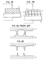
- Fig. 8A shows the generation of bridging between the electrode 2 and the workpiece 9 which frequently occurs when a copper electrode is employed.
- projections are formed on the electrode 2 and the workpiece 9 which can short-circuit the electrode to the workpiece 9.
- Fig. 8B because the machining gap is broader, there is no danger of shortcircuiting between the electrode 2 and the workpiece 9.
- the average distance on the surface of the electrode 2 and the workpiece 9 between projections is greater in the case of the electrode of the invention. Accordingly, there is less concentration of electric field, and thereby a more uniform discharge is produced.
Landscapes
- Engineering & Computer Science (AREA)
- Manufacturing & Machinery (AREA)
- Mechanical Engineering (AREA)
- Electrical Discharge Machining, Electrochemical Machining, And Combined Machining (AREA)
Applications Claiming Priority (2)
| Application Number | Priority Date | Filing Date | Title |
|---|---|---|---|
| JP15335184A JPS6133819A (ja) | 1984-07-24 | 1984-07-24 | 放電加工用電極 |
| JP153351/84 | 1984-07-24 |
Publications (2)
| Publication Number | Publication Date |
|---|---|
| EP0171668A1 true EP0171668A1 (de) | 1986-02-19 |
| EP0171668B1 EP0171668B1 (de) | 1990-10-03 |
Family
ID=15560564
Family Applications (1)
| Application Number | Title | Priority Date | Filing Date |
|---|---|---|---|
| EP85109250A Expired EP0171668B1 (de) | 1984-07-24 | 1985-07-24 | Elektroerosionselektrode |
Country Status (4)
| Country | Link |
|---|---|
| US (1) | US4952768A (de) |
| EP (1) | EP0171668B1 (de) |
| JP (1) | JPS6133819A (de) |
| DE (1) | DE3579980D1 (de) |
Families Citing this family (16)
| Publication number | Priority date | Publication date | Assignee | Title |
|---|---|---|---|---|
| JPH03184724A (ja) * | 1989-12-12 | 1991-08-12 | Tokai Carbon Co Ltd | 放電加工用電極材とその製造方法 |
| US5189276A (en) * | 1990-02-13 | 1993-02-23 | Mitsubishi Denki K.K. | Method and apparatus for treating the dielectric used in electrical discharge machining |
| US5434380A (en) * | 1990-07-16 | 1995-07-18 | Mitsubishi Denki Kabushiki Kaisha | Surface layer forming apparatus using electric discharge machining |
| US5369240A (en) * | 1992-02-05 | 1994-11-29 | Mitsubishi Denki Kabushiki Kaisha | Graphite matrix electrode with dispersed silicon particles |
| JP3393885B2 (ja) * | 1992-11-02 | 2003-04-07 | 信之 高橋 | 粉末分散放電加工液および放電加工法 |
| US5808262A (en) * | 1995-06-07 | 1998-09-15 | Swil Limited | Wire electrode for electro-discharge machining and method of manufacturing same |
| US5922221A (en) * | 1996-02-02 | 1999-07-13 | Sodick Co., Ltd. | Electric discharge machining method and electric discharge machining fluid |
| US5818005A (en) * | 1997-04-24 | 1998-10-06 | Motorola, Inc. | Electrical discharge machining electrode and rapid method for fabricating same |
| US6409902B1 (en) | 1999-08-06 | 2002-06-25 | New Jersey Institute Of Technology | Rapid production of engineering tools and hollow bodies by integration of electroforming and solid freeform fabrication |
| AU1571301A (en) | 1999-10-16 | 2001-04-30 | Paralax, Llc | Vacuum variable capacitor |
| US6586699B1 (en) * | 2002-02-20 | 2003-07-01 | Wisconsin Alumni Research Foundation | Micro-electro-discharge machining utilizing semiconductor electrodes |
| JP4575134B2 (ja) * | 2004-12-20 | 2010-11-04 | 株式会社ソディック | 放電加工用電極及び放電加工法 |
| US20080142488A1 (en) * | 2006-12-19 | 2008-06-19 | General Electric Company | Compound electrode, methods of manufacture thereof and articles comprising the same |
| JP5146461B2 (ja) * | 2007-11-19 | 2013-02-20 | 三菱電機株式会社 | 放電表面処理用電極およびそれを用いて成膜された金属被膜 |
| US20140017415A1 (en) * | 2012-07-13 | 2014-01-16 | General Electric Company | Coating/repairing process using electrospark with psp rod |
| CN103480925A (zh) * | 2013-09-27 | 2014-01-01 | 昆山纯柏精密五金有限公司 | 一种混粉电火花加工工艺 |
Citations (6)
| Publication number | Priority date | Publication date | Assignee | Title |
|---|---|---|---|---|
| DE403741C (de) * | 1923-03-16 | 1924-10-11 | Chile Exploration Company | Elektrode |
| DE1169057B (de) * | 1960-02-09 | 1964-04-30 | Centre Nat Rech Scient | Elektroerosions-Elektrode aus einem Gemisch eines feinverteilten leitenden Stoffes und eines nichtmetallischen Zusatzstoffes |
| DE1565362A1 (de) * | 1966-03-31 | 1970-02-05 | Aeg Elotherm Gmbh | Werkzeugelektrode fuer die elektrochemische Bearbeitung |
| CH512170A (de) * | 1967-04-17 | 1971-08-31 | Mitsubishi Steel Mfg | Elektrode und Verfahren zur Herstellung der Elektrode |
| DE2456515A1 (de) * | 1973-12-12 | 1975-06-19 | Philips Nv | Elektrode fuer elektrochemische bearbeitung |
| US4341939A (en) * | 1979-10-11 | 1982-07-27 | Ateliers Des Charmilles, S.A. | Wire electrode for cutting an electrode workpiece by electrical discharges |
Family Cites Families (16)
| Publication number | Priority date | Publication date | Assignee | Title |
|---|---|---|---|---|
| DE1061005B (de) * | 1952-11-24 | 1959-07-09 | Deutsche Edelstahlwerke Ag | Herstellung von Elektroden zur Funkenerosion |
| US2861164A (en) * | 1955-05-27 | 1958-11-18 | Republic Aviat Corp | Tool for electrical machining and the method of making and using the same |
| US3035151A (en) * | 1960-02-24 | 1962-05-15 | Budd Co | Spark machining electrodes and method of making the same |
| US3385947A (en) * | 1962-11-13 | 1968-05-28 | Inoue K | Apparatus for combined electrical dischargemachining and electrochemical machining |
| US3413435A (en) * | 1964-10-02 | 1968-11-26 | Rametco Inc | Electrical discharge machine electrodes impregnated with inorganic compounds |
| US3459915A (en) * | 1967-05-03 | 1969-08-05 | Mallory & Co Inc P R | Electrical discharge machining electrode comprising tungsten particles in a silver matrix |
| US3496987A (en) * | 1967-06-29 | 1970-02-24 | Avco Corp | Method of forming three-dimensional refractory shapes |
| US3689729A (en) * | 1969-12-04 | 1972-09-05 | Mor Wear Tools Inc | Electrode for electrical discharge machining |
| GB2015909B (en) * | 1978-03-03 | 1982-12-01 | Charmilles Sa Ateliers | Electrode for spark erosion machining |
| US4329219A (en) * | 1979-10-29 | 1982-05-11 | Druzhinin Ernest A | Electrode for electrochemical processes |
| JPS56114621A (en) * | 1980-02-05 | 1981-09-09 | Inoue Japax Res Inc | Wire-cut machining method by electric conduction |
| US4373127A (en) * | 1980-02-06 | 1983-02-08 | Minnesota Mining And Manufacturing Company | EDM Electrodes |
| JPS5733928A (en) * | 1980-07-29 | 1982-02-24 | Inoue Japax Res Inc | Carbon electrode for electric discharge machining |
| JPS5894925A (ja) * | 1981-11-26 | 1983-06-06 | Fanuc Ltd | 放電加工用ワイヤ電極 |
| JPH0610267B2 (ja) * | 1987-06-26 | 1994-02-09 | 日本電信電話株式会社 | 高分子薄膜及びその作製方法 |
| ES2021154B3 (es) * | 1987-11-25 | 1991-10-16 | Etablissements Mesnel Soc Anonyme Dite : | Perfil para la guia y la estanqueidad de un cristal movil, en particular de una puerta de automovil y procedimiento para su fabricacion. |
-
1984
- 1984-07-24 JP JP15335184A patent/JPS6133819A/ja active Pending
-
1985
- 1985-07-24 DE DE8585109250T patent/DE3579980D1/de not_active Expired - Lifetime
- 1985-07-24 EP EP85109250A patent/EP0171668B1/de not_active Expired
-
1988
- 1988-03-17 US US07/171,205 patent/US4952768A/en not_active Expired - Lifetime
Patent Citations (6)
| Publication number | Priority date | Publication date | Assignee | Title |
|---|---|---|---|---|
| DE403741C (de) * | 1923-03-16 | 1924-10-11 | Chile Exploration Company | Elektrode |
| DE1169057B (de) * | 1960-02-09 | 1964-04-30 | Centre Nat Rech Scient | Elektroerosions-Elektrode aus einem Gemisch eines feinverteilten leitenden Stoffes und eines nichtmetallischen Zusatzstoffes |
| DE1565362A1 (de) * | 1966-03-31 | 1970-02-05 | Aeg Elotherm Gmbh | Werkzeugelektrode fuer die elektrochemische Bearbeitung |
| CH512170A (de) * | 1967-04-17 | 1971-08-31 | Mitsubishi Steel Mfg | Elektrode und Verfahren zur Herstellung der Elektrode |
| DE2456515A1 (de) * | 1973-12-12 | 1975-06-19 | Philips Nv | Elektrode fuer elektrochemische bearbeitung |
| US4341939A (en) * | 1979-10-11 | 1982-07-27 | Ateliers Des Charmilles, S.A. | Wire electrode for cutting an electrode workpiece by electrical discharges |
Non-Patent Citations (2)
| Title |
|---|
| PATENT ABSTRACTS OF JAPAN, unexamined applications, M field, vol. 7, no. 283, December 16, 1983 THE PATENT OFFICE JAPANESE GOVERNMENT page 156 M 263 * JP - A - 58-160 019 ( FURUKAWA ) * * |
| PATENT ABSTRACTS OF JAPAN, unexamined applications, M section, vol. 3, no. 126, October 20, 1979 THE PATENT OFFICE JAPANESE GOVERNMENT page 152 M 77 * JP - A - 54-104 095 ( INOUE ) * * |
Also Published As
| Publication number | Publication date |
|---|---|
| US4952768A (en) | 1990-08-28 |
| EP0171668B1 (de) | 1990-10-03 |
| DE3579980D1 (de) | 1990-11-08 |
| JPS6133819A (ja) | 1986-02-17 |
Similar Documents
| Publication | Publication Date | Title |
|---|---|---|
| US4952768A (en) | Electric discharge machining electrode | |
| Wang et al. | Research on the influence of dielectric characteristics on the EDM of titanium alloy | |
| US4675644A (en) | Voltage-dependent resistor | |
| US5380341A (en) | Solid state electrochemical capacitors and their preparation | |
| Rhoney et al. | Wire electrical discharge machining of metal bond diamond wheels for ceramic grinding | |
| JPS6154534B2 (de) | ||
| EP0596660B1 (de) | Bearbeitungsflüssigkeit für Funkenerosionsmaschine | |
| EP1387392B1 (de) | Elektrostatischer Greifer | |
| EP0429653B1 (de) | Keramischer kondensator eines halbleitertyps mit laminierten und kornisolierten grenzschichten | |
| US3723690A (en) | Spark erosion of materials | |
| US4349496A (en) | Method for fabricating free-standing thick-film varistors | |
| EP0609888A1 (de) | Halbleitende Keramikmaterialien mit negativem Temperaturkoeffizienten des Widerstands | |
| US3742272A (en) | Spark suppressing brush brush holder assembly for rotating machines and sliding contacts | |
| JPH01156497A (ja) | 電着法による超電導性物品の形成方法 | |
| US4657818A (en) | Sliding current collector | |
| IE42714B1 (en) | Improvements in varistors | |
| US5369240A (en) | Graphite matrix electrode with dispersed silicon particles | |
| JPH0749170B2 (ja) | 放電加工による表面層の形成方法 | |
| Briffod et al. | Wire electrode for cutting an electrode workpiece by electrical discharges | |
| JPS61164718A (ja) | ワイヤカツト放電加工機 | |
| Spur et al. | Wire-Electroerosion of PCD Materials | |
| EP0883901A1 (de) | Mehrschichtige zno polykristalline diode | |
| WO2006068277A1 (ja) | 放電加工用電極および放電加工方法 | |
| Tamari et al. | Electrical Discharge Machining of Si sub 3 N sub 4--SiC Whisker Composite Ceramics | |
| SU1119815A1 (ru) | Способ электроэрозионного легировани |
Legal Events
| Date | Code | Title | Description |
|---|---|---|---|
| PUAI | Public reference made under article 153(3) epc to a published international application that has entered the european phase |
Free format text: ORIGINAL CODE: 0009012 |
|
| AK | Designated contracting states |
Designated state(s): CH DE GB LI |
|
| 17P | Request for examination filed |
Effective date: 19860626 |
|
| 17Q | First examination report despatched |
Effective date: 19870213 |
|
| GRAA | (expected) grant |
Free format text: ORIGINAL CODE: 0009210 |
|
| AK | Designated contracting states |
Kind code of ref document: B1 Designated state(s): CH DE GB LI |
|
| REF | Corresponds to: |
Ref document number: 3579980 Country of ref document: DE Date of ref document: 19901108 |
|
| PLBE | No opposition filed within time limit |
Free format text: ORIGINAL CODE: 0009261 |
|
| STAA | Information on the status of an ep patent application or granted ep patent |
Free format text: STATUS: NO OPPOSITION FILED WITHIN TIME LIMIT |
|
| 26N | No opposition filed | ||
| PGFP | Annual fee paid to national office [announced via postgrant information from national office to epo] |
Ref country code: GB Payment date: 19920713 Year of fee payment: 8 |
|
| PGFP | Annual fee paid to national office [announced via postgrant information from national office to epo] |
Ref country code: CH Payment date: 19920805 Year of fee payment: 8 |
|
| PGFP | Annual fee paid to national office [announced via postgrant information from national office to epo] |
Ref country code: DE Payment date: 19920818 Year of fee payment: 8 |
|
| PG25 | Lapsed in a contracting state [announced via postgrant information from national office to epo] |
Ref country code: GB Effective date: 19930724 |
|
| PG25 | Lapsed in a contracting state [announced via postgrant information from national office to epo] |
Ref country code: LI Effective date: 19930731 Ref country code: CH Effective date: 19930731 |
|
| GBPC | Gb: european patent ceased through non-payment of renewal fee |
Effective date: 19930724 |
|
| REG | Reference to a national code |
Ref country code: CH Ref legal event code: PL |
|
| PG25 | Lapsed in a contracting state [announced via postgrant information from national office to epo] |
Ref country code: DE Effective date: 19940401 |