EP0172572A2 - Schaltung zum Verarbeiten eines Synchronisierungssignals - Google Patents
Schaltung zum Verarbeiten eines Synchronisierungssignals Download PDFInfo
- Publication number
- EP0172572A2 EP0172572A2 EP85110527A EP85110527A EP0172572A2 EP 0172572 A2 EP0172572 A2 EP 0172572A2 EP 85110527 A EP85110527 A EP 85110527A EP 85110527 A EP85110527 A EP 85110527A EP 0172572 A2 EP0172572 A2 EP 0172572A2
- Authority
- EP
- European Patent Office
- Prior art keywords
- signal
- circuit
- synchronization signal
- video signal
- reproduction
- Prior art date
- Legal status (The legal status is an assumption and is not a legal conclusion. Google has not performed a legal analysis and makes no representation as to the accuracy of the status listed.)
- Granted
Links
Images


Classifications
-
- H—ELECTRICITY
- H04—ELECTRIC COMMUNICATION TECHNIQUE
- H04N—PICTORIAL COMMUNICATION, e.g. TELEVISION
- H04N5/00—Details of television systems
- H04N5/76—Television signal recording
- H04N5/91—Television signal processing therefor
- H04N5/93—Regeneration of the television signal or of selected parts thereof
-
- H—ELECTRICITY
- H04—ELECTRIC COMMUNICATION TECHNIQUE
- H04N—PICTORIAL COMMUNICATION, e.g. TELEVISION
- H04N5/00—Details of television systems
- H04N5/76—Television signal recording
- H04N5/91—Television signal processing therefor
- H04N5/915—Television signal processing therefor for field- or frame-skip recording or reproducing
- H04N5/9155—Television signal processing therefor for field- or frame-skip recording or reproducing with sound multiplexing
-
- H—ELECTRICITY
- H04—ELECTRIC COMMUNICATION TECHNIQUE
- H04N—PICTORIAL COMMUNICATION, e.g. TELEVISION
- H04N5/00—Details of television systems
- H04N5/76—Television signal recording
- H04N5/91—Television signal processing therefor
- H04N5/93—Regeneration of the television signal or of selected parts thereof
- H04N5/932—Regeneration of analogue synchronisation signals
Definitions
- one-half interlace scanning is adopted.
- one field is 262.5 H (H being the period of horizontal synchronization signal)
- one frame consists of 2 fields, i.e., 525 H.
- a reproducing signal from a video disk of the still video floppy system where the video data of one field, i.e., 262.5 H is recorded for each rotation of the disk
- there is a deviation of 0.5 H in the horizontal sync pulse i.e., one half the period of the horizontal synchronization signal
- the juncture i.e., start or end point
- a television synchronization signal waveform processing circuit which comprises a reproduction/demodulation circuit for reproducing a video signal by repeatedly reading out a video signal for one field from a video signal recording medium, generating the reproduced video signal and a sync signal separated from the reproduced composite video signal, a first delay circuit for delaying the reproduced video signal read out for every other field from the reproduction/demodulation circuit by one half period of the horizontal synchronization signal, a second delay circuit for delaying a vertical synchronization signal included in the separated sync signal from the reproduction/demodulation circuit by a predetermined period of time shorter than one half the period of the horizontal synchronization signal, and a waveform synthesis circuit for combining the outputs of the first and second delay circuits to produce a composite video signal used for effecting video display.
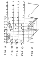
- Fig. 1A shows synchronization pulses in a reproduced signal. Labeled at V s are vertical synchronization pulses, and at H s horizontal synchronization pulses.
- V s vertical synchronization pulses
- H S horizontal synchronization pulses
- a synchronization pulse train as shown in Fig. 1B is obtained.
- FIG. 1B is as shown by imaginary line A in Fig. lE.
- a horizontal scanning line corresponding to a horizontal synchronization pulse in a field where the horizontal synchronization pulses are not delayed is at a position shown at a.
- a corresponding horizontal scanning line in a field where the horizontal synchronization pulses are delayed is at a position shown at b, which is deviated downwards in the Figure with respect to the position a. If this system is adopted, the image reproduction is vibrated vertically for every field.
- a synchronization pulse train as shown in Fig. 1D is obtained.
- a vertical scan sawtooth wave that is obtained with the vertical synchronization pulses V S3 in this pulse train is as shown by solid line C in Fig. lE.
- a horizontal scanning line corresponding to a horizontal synchronization pulse in a field where the synchronization pulses are not delayed is at a position shown at a, while a corresponding horizontal line in a field where the synchronization pulses are not delayed is at a position shown at d.
- the positions a and d are substantially alike, that is, a still image free from vertical vibrations can be obtained through processing of the synchronization pulse train in Fig. 1D.
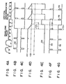
- the one-field composite video signal stored on the magnetic disk 11 is read out repeatedly at rate of 60 times a second, for instance, by a magnetic head 12 and then fed to a reproduction/demodulation circuit 13.
- the reproduction/demodulation circuit 13 feeds the input reproduced signal Sl to a first delay circuit 14.
- the circuit 13 includes a sync. separation circuit (not shown) which separates the synchronization signal S2 from the input reproduced signal and inverts the separated synchronization signal, the resultant signal being fed to a second delay circuit 15.
- the first delay circuit 14 includes a 0.5-H delay circuit 16, which delays the input signal by one half the period H of the horizontal synchronization signal, and a two- contact switch 17.
- the other terminal of the resistor 77 is connected to an input terminal 12, to which the reproduced signal noted above is supplied.
- the other terminal of the resistor 78 is connected to an output terminal OUT, from which the composite video signal is derived.
- the collector output of the second transistor 63 in the comparator 20 is fed through a resistor 79 to the base of the third transistor 75.
- This circuit is used where the synchronization signal S2 fed to the input terminal Il has the opposite polarity to that of the synchronization signal described before in connection with the previous embodiment, and the same effects as in the previous embodiment can be obtained with this circuit.
Landscapes
- Engineering & Computer Science (AREA)
- Multimedia (AREA)
- Signal Processing (AREA)
- Television Signal Processing For Recording (AREA)
- Synchronizing For Television (AREA)
Applications Claiming Priority (2)
| Application Number | Priority Date | Filing Date | Title |
|---|---|---|---|
| JP176279/84 | 1984-08-24 | ||
| JP59176279A JPS6154774A (ja) | 1984-08-24 | 1984-08-24 | テレビジヨン同期信号波形処理装置 |
Publications (3)
| Publication Number | Publication Date |
|---|---|
| EP0172572A2 true EP0172572A2 (de) | 1986-02-26 |
| EP0172572A3 EP0172572A3 (en) | 1988-09-14 |
| EP0172572B1 EP0172572B1 (de) | 1992-04-22 |
Family
ID=16010799
Family Applications (1)
| Application Number | Title | Priority Date | Filing Date |
|---|---|---|---|
| EP85110527A Expired - Lifetime EP0172572B1 (de) | 1984-08-24 | 1985-08-21 | Schaltung zum Verarbeiten eines Synchronisierungssignals |
Country Status (6)
| Country | Link |
|---|---|
| US (1) | US4675751A (de) |
| EP (1) | EP0172572B1 (de) |
| JP (1) | JPS6154774A (de) |
| KR (1) | KR860002204A (de) |
| CA (1) | CA1238975A (de) |
| DE (1) | DE3585898D1 (de) |
Cited By (1)
| Publication number | Priority date | Publication date | Assignee | Title |
|---|---|---|---|---|
| GB2319683A (en) * | 1996-11-19 | 1998-05-27 | Digi Media Vision Ltd | Apparatus to decode an input video signal |
Families Citing this family (4)
| Publication number | Priority date | Publication date | Assignee | Title |
|---|---|---|---|---|
| JPS61234683A (ja) * | 1985-04-10 | 1986-10-18 | Fuji Photo Film Co Ltd | フイ−ルド/フレ−ム変換におけるフリツカ防止回路 |
| JPH0789668B2 (ja) * | 1985-09-20 | 1995-09-27 | キヤノン株式会社 | 映像信号再生装置 |
| US4873581A (en) * | 1986-05-08 | 1989-10-10 | Fuji Photo Film Co. Ltd. | Field/frame conversion circuit |
| US4849828A (en) * | 1986-08-22 | 1989-07-18 | Pioneer Electronic Corporation | Search system and special reproduction system for information reproduction device |
Family Cites Families (7)
| Publication number | Priority date | Publication date | Assignee | Title |
|---|---|---|---|---|
| US3777054A (en) * | 1972-03-13 | 1973-12-04 | Avco Corp | Vertical synchronization time base error corrector |
| JPS5413938B2 (de) * | 1973-07-24 | 1979-06-04 | ||
| US4058840A (en) * | 1975-11-26 | 1977-11-15 | Arvin Industries, Inc. | Method and apparatus for recording a single video frame |
| US4027333A (en) * | 1975-12-09 | 1977-05-31 | Cbs Inc. | Multiplex color television transmission system |
| US4153917A (en) * | 1978-01-23 | 1979-05-08 | The United States Of America As Represented By The Secretary Of The Navy | Image stabilizer system for stop-action playback |
| JPS5511618A (en) * | 1978-07-10 | 1980-01-26 | Victor Co Of Japan Ltd | Reproduced signal process system for rotary magnetic medium recorder/reproducer |
| CA1204209A (en) * | 1981-10-27 | 1986-05-06 | Hisao Kinjo | Recording medium for recording and/or reproducing apparatus |
-
1984
- 1984-08-24 JP JP59176279A patent/JPS6154774A/ja not_active Expired - Lifetime
-
1985
- 1985-08-19 US US06/767,162 patent/US4675751A/en not_active Expired - Fee Related
- 1985-08-20 KR KR1019850005989A patent/KR860002204A/ko not_active Ceased
- 1985-08-21 DE DE8585110527T patent/DE3585898D1/de not_active Expired - Lifetime
- 1985-08-21 EP EP85110527A patent/EP0172572B1/de not_active Expired - Lifetime
- 1985-08-21 CA CA000489113A patent/CA1238975A/en not_active Expired
Cited By (1)
| Publication number | Priority date | Publication date | Assignee | Title |
|---|---|---|---|---|
| GB2319683A (en) * | 1996-11-19 | 1998-05-27 | Digi Media Vision Ltd | Apparatus to decode an input video signal |
Also Published As
| Publication number | Publication date |
|---|---|
| DE3585898D1 (de) | 1992-05-27 |
| US4675751A (en) | 1987-06-23 |
| KR860002204A (ko) | 1986-03-26 |
| EP0172572B1 (de) | 1992-04-22 |
| JPS6154774A (ja) | 1986-03-19 |
| CA1238975A (en) | 1988-07-05 |
| EP0172572A3 (en) | 1988-09-14 |
Similar Documents
| Publication | Publication Date | Title |
|---|---|---|
| US4364090A (en) | Method for a compatible increase in resolution in television systems | |
| US4451848A (en) | Television receiver including a circuit for doubling line scanning frequency | |
| US5414463A (en) | Video cameras capable of switching an aspect ratio and view finders for use in the same | |
| US4549224A (en) | Digital video tape recorder that can be used with different television systems | |
| EP0227071B1 (de) | Vorrichtung zum Abspielen von Videoplatten | |
| US4675751A (en) | Processing circuit for television sync signals produced from a recording medium for performing a non-interlaced display | |
| US4481543A (en) | Playback apparatus for producing still images | |
| JPH04271685A (ja) | 同期信号復元回路 | |
| JP2651012B2 (ja) | テレビジョン受像機 | |
| EP0515155B1 (de) | Abtastratenumwandlung | |
| US3990107A (en) | Circuit for automatically controlling horizontal scanning frequency | |
| US4766506A (en) | Processing circuit for television sync signals produced from a recording medium for preforming a non-interlaced display | |
| EP0631437B1 (de) | System zur Aufzeichnung von Teletextdaten | |
| EP0584824A2 (de) | Für Bild-im-Bild-System geeignete Oszillatorschaltung | |
| US4524387A (en) | Synchronization input for television receiver on-screen alphanumeric display | |
| GB2248745A (en) | Picture signal superposing circuit | |
| EP0865198B1 (de) | Verfahren und Vorrichtung zur Anordnung von digitalisierten Bildsignalen oder Daten in orthogonalen Reihen und Spalten | |
| US5309291A (en) | Circuit for compensating the errors occurring when changing the playing back speed of a double azimuth 4-head VTR | |
| JP2758190B2 (ja) | 画像再生の画質改良のための,順次−インターレース走査変換方法及び装置 | |
| JPH01194784A (ja) | テレビジョン受像機 | |
| KR880004356Y1 (ko) | Vtr의 강제 동기신호 발생회로 | |
| JP2615749B2 (ja) | テレビジョン受像機 | |
| JP3086749B2 (ja) | ビデオ機器用相加平均装置 | |
| JPH0134512B2 (de) | ||
| JP2783609B2 (ja) | 画像信号処理装置 |
Legal Events
| Date | Code | Title | Description |
|---|---|---|---|
| PUAI | Public reference made under article 153(3) epc to a published international application that has entered the european phase |
Free format text: ORIGINAL CODE: 0009012 |
|
| AK | Designated contracting states |
Designated state(s): DE FR GB IT NL SE |
|
| PUAL | Search report despatched |
Free format text: ORIGINAL CODE: 0009013 |
|
| AK | Designated contracting states |
Kind code of ref document: A3 Designated state(s): DE FR GB IT NL SE |
|
| 17P | Request for examination filed |
Effective date: 19890213 |
|
| 17Q | First examination report despatched |
Effective date: 19910729 |
|
| GRAA | (expected) grant |
Free format text: ORIGINAL CODE: 0009210 |
|
| AK | Designated contracting states |
Kind code of ref document: B1 Designated state(s): DE FR GB IT NL SE |
|
| ITF | It: translation for a ep patent filed | ||
| REF | Corresponds to: |
Ref document number: 3585898 Country of ref document: DE Date of ref document: 19920527 |
|
| PGFP | Annual fee paid to national office [announced via postgrant information from national office to epo] |
Ref country code: FR Payment date: 19920713 Year of fee payment: 8 |
|
| ET | Fr: translation filed | ||
| PGFP | Annual fee paid to national office [announced via postgrant information from national office to epo] |
Ref country code: GB Payment date: 19920807 Year of fee payment: 8 |
|
| PGFP | Annual fee paid to national office [announced via postgrant information from national office to epo] |
Ref country code: SE Payment date: 19920818 Year of fee payment: 8 |
|
| ITTA | It: last paid annual fee | ||
| PGFP | Annual fee paid to national office [announced via postgrant information from national office to epo] |
Ref country code: NL Payment date: 19920831 Year of fee payment: 8 |
|
| PGFP | Annual fee paid to national office [announced via postgrant information from national office to epo] |
Ref country code: DE Payment date: 19921030 Year of fee payment: 8 |
|
| PLBE | No opposition filed within time limit |
Free format text: ORIGINAL CODE: 0009261 |
|
| STAA | Information on the status of an ep patent application or granted ep patent |
Free format text: STATUS: NO OPPOSITION FILED WITHIN TIME LIMIT |
|
| 26N | No opposition filed | ||
| PG25 | Lapsed in a contracting state [announced via postgrant information from national office to epo] |
Ref country code: GB Effective date: 19930821 |
|
| PG25 | Lapsed in a contracting state [announced via postgrant information from national office to epo] |
Ref country code: SE Effective date: 19930822 |
|
| PG25 | Lapsed in a contracting state [announced via postgrant information from national office to epo] |
Ref country code: NL Effective date: 19940301 |
|
| NLV4 | Nl: lapsed or anulled due to non-payment of the annual fee | ||
| GBPC | Gb: european patent ceased through non-payment of renewal fee |
Effective date: 19930821 |
|
| PG25 | Lapsed in a contracting state [announced via postgrant information from national office to epo] |
Ref country code: FR Effective date: 19940429 |
|
| PG25 | Lapsed in a contracting state [announced via postgrant information from national office to epo] |
Ref country code: DE Effective date: 19940503 |
|
| REG | Reference to a national code |
Ref country code: FR Ref legal event code: ST |
|
| EUG | Se: european patent has lapsed |
Ref document number: 85110527.0 Effective date: 19940310 |