EP0173368A2 - Dispositif de production thermique d'images et procédé pour la fabrication d'un dispositif de production thermique d'images - Google Patents
Dispositif de production thermique d'images et procédé pour la fabrication d'un dispositif de production thermique d'images Download PDFInfo
- Publication number
- EP0173368A2 EP0173368A2 EP85201175A EP85201175A EP0173368A2 EP 0173368 A2 EP0173368 A2 EP 0173368A2 EP 85201175 A EP85201175 A EP 85201175A EP 85201175 A EP85201175 A EP 85201175A EP 0173368 A2 EP0173368 A2 EP 0173368A2
- Authority
- EP
- European Patent Office
- Prior art keywords
- ferroelectric
- electrically conductive
- insulating material
- main surface
- layer
- Prior art date
- Legal status (The legal status is an assumption and is not a legal conclusion. Google has not performed a legal analysis and makes no representation as to the accuracy of the status listed.)
- Withdrawn
Links
Images

Classifications
-
- G—PHYSICS
- G01—MEASURING; TESTING
- G01J—MEASUREMENT OF INTENSITY, VELOCITY, SPECTRAL CONTENT, POLARISATION, PHASE OR PULSE CHARACTERISTICS OF INFRARED, VISIBLE OR ULTRAVIOLET LIGHT; COLORIMETRY; RADIATION PYROMETRY
- G01J5/00—Radiation pyrometry, e.g. infrared or optical thermometry
- G01J5/10—Radiation pyrometry, e.g. infrared or optical thermometry using electric radiation detectors
- G01J5/34—Radiation pyrometry, e.g. infrared or optical thermometry using electric radiation detectors using capacitors, e.g. pyroelectric capacitors
-
- H—ELECTRICITY
- H10—SEMICONDUCTOR DEVICES; ELECTRIC SOLID-STATE DEVICES NOT OTHERWISE PROVIDED FOR
- H10N—ELECTRIC SOLID-STATE DEVICES NOT OTHERWISE PROVIDED FOR
- H10N15/00—Thermoelectric devices without a junction of dissimilar materials; Thermomagnetic devices, e.g. using the Nernst-Ettingshausen effect
- H10N15/10—Thermoelectric devices using thermal change of the dielectric constant, e.g. working above and below the Curie point
-
- Y—GENERAL TAGGING OF NEW TECHNOLOGICAL DEVELOPMENTS; GENERAL TAGGING OF CROSS-SECTIONAL TECHNOLOGIES SPANNING OVER SEVERAL SECTIONS OF THE IPC; TECHNICAL SUBJECTS COVERED BY FORMER USPC CROSS-REFERENCE ART COLLECTIONS [XRACs] AND DIGESTS
- Y10—TECHNICAL SUBJECTS COVERED BY FORMER USPC
- Y10T—TECHNICAL SUBJECTS COVERED BY FORMER US CLASSIFICATION
- Y10T29/00—Metal working
- Y10T29/42—Piezoelectric device making
-
- Y—GENERAL TAGGING OF NEW TECHNOLOGICAL DEVELOPMENTS; GENERAL TAGGING OF CROSS-SECTIONAL TECHNOLOGIES SPANNING OVER SEVERAL SECTIONS OF THE IPC; TECHNICAL SUBJECTS COVERED BY FORMER USPC CROSS-REFERENCE ART COLLECTIONS [XRACs] AND DIGESTS
- Y10—TECHNICAL SUBJECTS COVERED BY FORMER USPC
- Y10T—TECHNICAL SUBJECTS COVERED BY FORMER US CLASSIFICATION
- Y10T29/00—Metal working
- Y10T29/49—Method of mechanical manufacture
- Y10T29/49002—Electrical device making
- Y10T29/49117—Conductor or circuit manufacturing
- Y10T29/49124—On flat or curved insulated base, e.g., printed circuit, etc.
- Y10T29/4913—Assembling to base an electrical component, e.g., capacitor, etc.
- Y10T29/49144—Assembling to base an electrical component, e.g., capacitor, etc. by metal fusion
Definitions
- the invention relates to a thermal imaging device comprising a slab of ferroelectric or pyroelectric material bearing an infra-red-permeable common electrode on one main surface and a signal electrode structure on the opposite main surface, the signal electrode structure being electrically connected to electrodes of a circuit substrate by means of conductors surrounded by a thermally insulating material.
- the present invention also provides a method of manufacturing a thermal imaging device, which method comprises the steps of providing a slab of ferroelectric or pyroelectric material with an infra-red-permeable common electrode on one main surface and with a signal electrode layer on the opposite main surface.
- a significant problem with such devices is to provide adequate mechanical support for the slab of ferroelectric material, while at the same time providing good thermal isolation between adjacent sensing regions and between the sensing regions of the device and the circuit substrate, which is, for example, an electronic multiplexer.
- United States Patent Specification 4,143,269 describes a ferroelectric imaging system in which the conductors are conductor rods which are either in a vacuum, in which case it does not appear that the conductor structure per se will provide adequate mechanical support for the ferroelectric slab, or are embedded in a mass of thermally insulating material, for example, of a glass-filled photoresist.
- the conductor rods are embedded in such a mass of thermally insulating material, there is still a heat flow between adjacent detector elements in the device in a direction transverse to the longitudinal axes of the conductors, and this has two effects which impair the device performance. Firstly there is a degradation of the thermal limits of detection, thus the transverse heat conductance provides a significant contribution to the signal produced by a given sensing element. And secondly, the transverse flow of heat can cause thermal cross-talk between adjacent elements.
- An object of the invention is to mitigate these problems.
- each conductor is a metal coating on a bore in a respective pillar of the insulating material.
- the invention also relates to a thermal imaging device comprising an integral array of ferroelectric or pyroelectric plates, each plate bearing a respective infra-red-permeable electrode on one main surface and a respective signal electrode on the opposite main surface, wherein adjacent plates are interconnected at their edges by means of anelectrically and thermally insulating material, the signal electrodes being electrically connected to respective electrodes of a circuit substrate by means of conductors surrounded by a thermally insulating material, characterized in that each conductor is a metal coating on a bore in a respective pillar of the insulating material.
- a method according to the present invention of manufacturing a thermal imaging device is characterized in that a sheet of thermally insulating material is bonded to the signal electrode layer, an electrically conductive layer is provided on the insulating sheet, a first photoresist layer is provided on the electrically conductive layer, the first photoresist layer is exposed and the exposed photoresist is developed so as to form an array of spaced apertures, bores disposed in accordance with this array are etched down to the signal electrode layer, an electrically conductive coating is provided on the surface of each bore so as to electrically connect the signal electrode layer to the electrically conductive layer on the insulating sheet, the remainder of the first photoresist layer and any superposed electrically conductive coating material are removed, a second photoresist layer is provided on the electrically conductive layer on the insulating sheet so as to close the open ends of the bores, the second photoresist layer is exposed and the exposed resist is developed so as to form a pattern of channels which define islands of photoresist, wherein I each
- the ferroelectric material may be, for example, a lead zirconate titanate, a barium strontium titanate, or a potassium tantaloniobate.
- Triglycine sulphate is an example of a suitable pyroelectric material.
- the thermally insulating material may be, for example, cadmium telluride, tellurium, selenium or sulphur.
- the thermally insulating sheet may be bonded to the signal electrode material, for example, by a thermosetting adhesive, for example, an epoxy resin.
- the infra-red-permeable electrode material may be, for example, chromium or a nickel-chromium alloy.
- the bores and channels may be formed, for example, by ion beam milling or reactive ion etching.
- a stack of thermally insulating plates bonded together by means of adhesive films which are disposed one between each pair of opposed sheets, may be used to improve the thermal isolation of the thermal imaging array from the circuit substrate.
- the transverse flow of heat between sensing elements may be further reduced by increasing the size of the bores of the plates in the stack from the bores in the plate nearest to the signal electrode layer to the bores in the plate nearest to the circuit substrate.
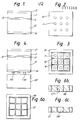
- a 6pm thick ferroelectric slab 1 of lead zirconate titanate was provided with an infra-red-permeable electrically conductive layer 2 of nickel-chromium having a surface resistance of 300JL per square on one main surface and an electrode layer 3 of nickel-chromium having a surface resistance of 60 ⁇ per square on the opposite main surface. Both of the layers 2 and 3 were formed by sputtering using a planar magnetron.
- a 17 pm thick thermally insulating sheet 4 of cadmium telluride was then bonded to the electrode layer 3 by means of a 1 ⁇ m thick epoxy resin film 5.
- a 3 pm thick indium layer 6 was provided on the exposed main surface of the insulating sheet 4. The thickness of each of the layers 2, 3 and 6 and of the film 5 have been greatly exaggerated in the drawings for the sake of clarity.
- a first photoresist layer (not shown) was then provided on the exposed main surface of the indium layer 6, and an array of 10 pm diameter holes spaced at a pitch of 40 pm was formed in the photoresist layer by exposure through a suitable mask and then developing the exposed photoresist.
- a pattern of blind bores 7 ( Figure 2) which each extended down to the nickel-chromium layer 3 was produced by ion beam milling in argon.
- Conductors 8 ( Figure 5) were formed in each of the bores 7 by sputtering 0.3 Vim thick composite layers of chromium (0.02 um) and gold (0.28 pm) using a planar magnetron. The remainder of the first photoresist layer and the superposed chromium-gold composite were then lifted off the indium layer 6.
- a second photoresist layer (not shown) was applied to the exposed indium layer and closed the open ends of the bores 7.
- a grid-shaped pattern was then formed in the second photoresist layer by exposure through a suitable mask followed by development of the exposed photoresist.
- 10 pm wide channels 9 ( Figure 3) which extended down to the ferroelectric slab 1 were formed by ion beam milling.
- These channels 9 defined insulating pillars 10 ( Figure 3) each having a cross-section of 30 pm x 30 pm, each pillar 10 surrounding a bore 7, and the channels 9 also defined signal electrodes 11 having external cross-sections similar to those of the pillars 10.
- the thermal imaging array produced as described with reference to Figures 1 to 4 was then secured to electrodes 12 of a circuit substrate 13 in the form of a CCD by means of indium bumps 14 which extended into respective bores 7 and were fused to the conductors 8 and to the exposed surface of the indium layer 6.
- a grid of slots 15 was etched by ion beam milling to a depth of 6 pm in a 9 pm thick lead zirconate titanate slab 16. These slots 15 were then filled with an epoxy resin 17 (Figure 6b) and the continuous main surface of the slab 16 was ground until the epoxy resin 17 was exposed.
- the integral array of ferroelectric plates 18 ( Figure 6c) was then used to make a thermal imaging device, part of which is shown in Figure 7, by performing the relevant process steps described in Example 1 with respect to Figures 1 to 5.
- the channels 9 which define the pillars 10 were in registration with the resin-filled grooves 15 which define the ferroelectric plates 18.
Landscapes
- Engineering & Computer Science (AREA)
- Power Engineering (AREA)
- Physics & Mathematics (AREA)
- General Physics & Mathematics (AREA)
- Spectroscopy & Molecular Physics (AREA)
- Radiation Pyrometers (AREA)
- Solid State Image Pick-Up Elements (AREA)
- Transforming Light Signals Into Electric Signals (AREA)
- Photometry And Measurement Of Optical Pulse Characteristics (AREA)
Applications Claiming Priority (2)
| Application Number | Priority Date | Filing Date | Title |
|---|---|---|---|
| GB8421506 | 1984-08-24 | ||
| GB08421506A GB2163596B (en) | 1984-08-24 | 1984-08-24 | A thermal imaging device and a method of manufacturing a thermal imaging device |
Publications (2)
| Publication Number | Publication Date |
|---|---|
| EP0173368A2 true EP0173368A2 (fr) | 1986-03-05 |
| EP0173368A3 EP0173368A3 (fr) | 1988-12-14 |
Family
ID=10565775
Family Applications (1)
| Application Number | Title | Priority Date | Filing Date |
|---|---|---|---|
| EP85201175A Withdrawn EP0173368A3 (fr) | 1984-08-24 | 1985-07-12 | Dispositif de production thermique d'images et procédé pour la fabrication d'un dispositif de production thermique d'images |
Country Status (5)
| Country | Link |
|---|---|
| US (2) | US4663529A (fr) |
| EP (1) | EP0173368A3 (fr) |
| JP (1) | JPS6178283A (fr) |
| GB (1) | GB2163596B (fr) |
| IL (1) | IL76151A0 (fr) |
Cited By (8)
| Publication number | Priority date | Publication date | Assignee | Title |
|---|---|---|---|---|
| EP0284131A1 (fr) * | 1987-03-13 | 1988-09-28 | Philips Electronics Uk Limited | Détecteur d'image thermique et son procédé de fabrication |
| US4894544A (en) * | 1987-07-10 | 1990-01-16 | U.S. Philips Corp. | Arrays of infrared detector elements |
| FR2639784A1 (fr) * | 1988-11-29 | 1990-06-01 | Commissariat Energie Atomique | Structure monolithique de detection ou d'imagerie infrarouge et son procede de fabrication |
| EP0345050A3 (en) * | 1988-06-01 | 1990-10-03 | Thorn Emi Electronics Limited | Thermal imaging device |
| EP0345047A3 (en) * | 1988-06-01 | 1990-10-03 | Thorn Emi Plc | Thermal imaging device |
| EP0345049A3 (en) * | 1988-06-01 | 1990-10-03 | Thorn Emi Electronics Limited | Thermal imaging device |
| EP0373807A3 (fr) * | 1988-12-13 | 1990-10-24 | Pilkington Thorn Optronics Limited | Dispositif der prise d'images thermiques |
| US5070026A (en) * | 1989-06-26 | 1991-12-03 | Spire Corporation | Process of making a ferroelectric electronic component and product |
Families Citing this family (25)
| Publication number | Priority date | Publication date | Assignee | Title |
|---|---|---|---|---|
| GB2163596B (en) * | 1984-08-24 | 1988-02-03 | Philips Electronic Associated | A thermal imaging device and a method of manufacturing a thermal imaging device |
| GB2200246B (en) * | 1985-09-12 | 1989-11-01 | Plessey Co Plc | Thermal detector array |
| GB2200245B (en) * | 1985-09-12 | 1989-09-13 | Plessey Co Plc | Thermal detector |
| US4988884A (en) * | 1988-11-22 | 1991-01-29 | Walter Kidde Aerospace, Inc. | High temperature resistant flame detector |
| GB8900688D0 (en) * | 1989-01-12 | 1989-07-05 | Thorn Emi Electronics Ltd | Thermal imaging device |
| US5047644A (en) * | 1989-07-31 | 1991-09-10 | Texas Instruments Incorporated | Polyimide thermal isolation mesa for a thermal imaging system |
| GB2236016A (en) * | 1989-09-13 | 1991-03-20 | Philips Electronic Associated | Pyroelectric and other infrared detection devices with thin films |
| US5306912A (en) * | 1989-10-21 | 1994-04-26 | Thorn Emi Plc | Optically addressed thermal imaging device |
| US5015858A (en) * | 1990-03-27 | 1991-05-14 | Hughes Aircraft Company | Thermally isolated focal plane readout |
| US5075549A (en) * | 1990-12-11 | 1991-12-24 | Hughes Aircraft Company | Pyroelectric detector using electronic chopping |
| US5384267A (en) * | 1993-10-19 | 1995-01-24 | Texas Instruments Incorporated | Method of forming infrared detector by hydrogen plasma etching to form refractory metal interconnects |
| US5370301A (en) * | 1994-01-04 | 1994-12-06 | Texas Instruments Incorporated | Apparatus and method for flip-chip bonding |
| US5351876A (en) * | 1994-01-04 | 1994-10-04 | Texas Instruments Incorporated | Apparatus and method for flip-clip bonding |
| US5485010A (en) * | 1994-01-13 | 1996-01-16 | Texas Instruments Incorporated | Thermal isolation structure for hybrid thermal imaging system |
| US5587090A (en) * | 1994-04-04 | 1996-12-24 | Texas Instruments Incorporated | Multiple level mask for patterning of ceramic materials |
| US5478242A (en) * | 1994-04-29 | 1995-12-26 | Texas Instruments Incorporated | Thermal isolation of hybrid thermal detectors through an anisotropic etch |
| JPH08148702A (ja) * | 1994-11-18 | 1996-06-07 | Sumitomo Metal Mining Co Ltd | 赤外線検知器 |
| US5644838A (en) * | 1995-01-03 | 1997-07-08 | Texas Instruments Incorporated | Method of fabricating a focal plane array for hybrid thermal imaging system |
| US5746930A (en) * | 1995-01-03 | 1998-05-05 | Texas Instruments Incorporated | Method and structure for forming an array of thermal sensors |
| US5626773A (en) * | 1995-01-03 | 1997-05-06 | Texas Instruments Incorporated | Structure and method including dry etching techniques for forming an array of thermal sensitive elements |
| US5603848A (en) * | 1995-01-03 | 1997-02-18 | Texas Instruments Incorporated | Method for etching through a substrate to an attached coating |
| GB9710843D0 (en) * | 1997-05-28 | 1997-07-23 | Secr Defence | A thermal detector array |
| WO1999019900A2 (fr) * | 1997-10-14 | 1999-04-22 | Patterning Technologies Limited | Procede de formation d'un dispositif electronique |
| US7323634B2 (en) * | 1998-10-14 | 2008-01-29 | Patterning Technologies Limited | Method of forming an electronic device |
| WO2010118036A1 (fr) * | 2009-04-06 | 2010-10-14 | Bridge Semiconductor Corporation | Interconnexion et système la comprenant |
Family Cites Families (10)
| Publication number | Priority date | Publication date | Assignee | Title |
|---|---|---|---|---|
| US4009516A (en) * | 1976-03-29 | 1977-03-01 | Honeywell Inc. | Pyroelectric detector fabrication |
| US4143269A (en) * | 1977-12-19 | 1979-03-06 | Texas Instruments Incorporated | Ferroelectric imaging system |
| US4449044A (en) * | 1979-02-26 | 1984-05-15 | Carson Alexion Corporation | Focal plane photo-detector mosaic array apparatus |
| US4383174A (en) * | 1979-09-25 | 1983-05-10 | Tokyo Shibaura Denki Kabushiki Kaisha | Pyroelectric detector and method for manufacturing the same |
| JPS5677730A (en) * | 1979-11-28 | 1981-06-26 | Sanyo Electric Co Ltd | Pyroelectric infrared-ray detector |
| US4354109A (en) * | 1979-12-31 | 1982-10-12 | Honeywell Inc. | Mounting for pyroelectric detecctor arrays |
| US4593456A (en) * | 1983-04-25 | 1986-06-10 | Rockwell International Corporation | Pyroelectric thermal detector array |
| US4532424A (en) * | 1983-04-25 | 1985-07-30 | Rockwell International Corporation | Pyroelectric thermal detector array |
| GB2143081B (en) * | 1983-07-06 | 1987-01-14 | Philips Electronic Associated | Infra-red detector with differentially connected pyroelecric elements |
| GB2163596B (en) * | 1984-08-24 | 1988-02-03 | Philips Electronic Associated | A thermal imaging device and a method of manufacturing a thermal imaging device |
-
1984
- 1984-08-24 GB GB08421506A patent/GB2163596B/en not_active Expired
-
1985
- 1985-07-12 EP EP85201175A patent/EP0173368A3/fr not_active Withdrawn
- 1985-07-29 US US06/759,997 patent/US4663529A/en not_active Expired - Fee Related
- 1985-08-21 JP JP60181922A patent/JPS6178283A/ja active Pending
- 1985-08-21 IL IL76151A patent/IL76151A0/xx not_active IP Right Cessation
-
1986
- 1986-10-20 US US06/920,647 patent/US4815199A/en not_active Expired - Fee Related
Cited By (10)
| Publication number | Priority date | Publication date | Assignee | Title |
|---|---|---|---|---|
| EP0284131A1 (fr) * | 1987-03-13 | 1988-09-28 | Philips Electronics Uk Limited | Détecteur d'image thermique et son procédé de fabrication |
| US4894544A (en) * | 1987-07-10 | 1990-01-16 | U.S. Philips Corp. | Arrays of infrared detector elements |
| EP0345050A3 (en) * | 1988-06-01 | 1990-10-03 | Thorn Emi Electronics Limited | Thermal imaging device |
| EP0345047A3 (en) * | 1988-06-01 | 1990-10-03 | Thorn Emi Plc | Thermal imaging device |
| EP0345049A3 (en) * | 1988-06-01 | 1990-10-03 | Thorn Emi Electronics Limited | Thermal imaging device |
| FR2639784A1 (fr) * | 1988-11-29 | 1990-06-01 | Commissariat Energie Atomique | Structure monolithique de detection ou d'imagerie infrarouge et son procede de fabrication |
| EP0371868A1 (fr) * | 1988-11-29 | 1990-06-06 | Commissariat A L'energie Atomique | Structure monolithique de détection ou d'imagerie infrarouge et son procédé de fabrication |
| US5008541A (en) * | 1988-11-29 | 1991-04-16 | Commissariat A L'energie Atomique | Monolithic detection or infrared imaging structure and its production process |
| EP0373807A3 (fr) * | 1988-12-13 | 1990-10-24 | Pilkington Thorn Optronics Limited | Dispositif der prise d'images thermiques |
| US5070026A (en) * | 1989-06-26 | 1991-12-03 | Spire Corporation | Process of making a ferroelectric electronic component and product |
Also Published As
| Publication number | Publication date |
|---|---|
| GB2163596A (en) | 1986-02-26 |
| JPS6178283A (ja) | 1986-04-21 |
| EP0173368A3 (fr) | 1988-12-14 |
| US4815199A (en) | 1989-03-28 |
| US4663529A (en) | 1987-05-05 |
| IL76151A0 (en) | 1985-12-31 |
| GB2163596B (en) | 1988-02-03 |
Similar Documents
| Publication | Publication Date | Title |
|---|---|---|
| EP0173368A2 (fr) | Dispositif de production thermique d'images et procédé pour la fabrication d'un dispositif de production thermique d'images | |
| US5047644A (en) | Polyimide thermal isolation mesa for a thermal imaging system | |
| US4300115A (en) | Multilayer via resistors | |
| DE69011224T2 (de) | Herstellung von elektrischen Messwandlern, speziell von Infrarotdetektorarrays. | |
| EP0284131B1 (fr) | Détecteur d'image thermique et son procédé de fabrication | |
| US5264326A (en) | Polyimide thermal isolation mesa for a thermal imaging system | |
| US3423260A (en) | Method of making a thin film circuit having a resistor-conductor pattern | |
| EP0628211A1 (fr) | Fusibles montes en surface, en film mince. | |
| US5572029A (en) | Thermal isolation for hybrid thermal detectors | |
| EP0663696B1 (fr) | Dispositif d'imagerie thermique | |
| DE10213827A1 (de) | Fluidströmungssensor und Verfahren zum Herstellen desselben | |
| US3671819A (en) | Metal-insulator structures and method for forming | |
| CA1208960A (fr) | Methode de fabrication de barrieres ameliorees pour dispositifs a effet josephson | |
| EP0345047B1 (fr) | Dispositif de prise d'images thermiques | |
| EP0148506B1 (fr) | Support de circuit | |
| EP0147566B1 (fr) | Procédé de fabrication de contacts pour supports flexibles de modules | |
| US4570329A (en) | Apparatus and method for fabricating backside mosaic of photoconductive infrared detectors | |
| US5152868A (en) | Elastomer connector for integrated circuits or similar, and method of manufacturing same | |
| DE4023776C2 (de) | Mehrschichtige Halbleiterstruktur, insbesondere Wandler und Verfahren zur Bildung von Kontaktflächen an Halbleiterbereichen solcher mehrschichtiger Halbleiterstrukturen | |
| US5314788A (en) | Matrix printed board and process of forming the same | |
| EP0608067B1 (fr) | Détecteur à infrarouge | |
| JP2752305B2 (ja) | 回路基板 | |
| JP2938341B2 (ja) | 同軸構造の配線の形成方法 | |
| US7390742B2 (en) | Method for producing a rewiring printed circuit board | |
| US3405276A (en) | Image intensifier comprising perforated glass substrate and method of making same |
Legal Events
| Date | Code | Title | Description |
|---|---|---|---|
| PUAI | Public reference made under article 153(3) epc to a published international application that has entered the european phase |
Free format text: ORIGINAL CODE: 0009012 |
|
| AK | Designated contracting states |
Kind code of ref document: A2 Designated state(s): DE FR GB IT |
|
| RAP3 | Party data changed (applicant data changed or rights of an application transferred) |
Owner name: N.V. PHILIPS' GLOEILAMPENFABRIEKEN Owner name: PHILIPS ELECTRONIC AND ASSOCIATED INDUSTRIES LIMIT |
|
| PUAL | Search report despatched |
Free format text: ORIGINAL CODE: 0009013 |
|
| AK | Designated contracting states |
Kind code of ref document: A3 Designated state(s): DE FR GB IT |
|
| 17P | Request for examination filed |
Effective date: 19890605 |
|
| 17Q | First examination report despatched |
Effective date: 19911205 |
|
| RAP3 | Party data changed (applicant data changed or rights of an application transferred) |
Owner name: N.V. PHILIPS' GLOEILAMPENFABRIEKEN Owner name: PHILIPS ELECTRONICS UK LIMITED |
|
| STAA | Information on the status of an ep patent application or granted ep patent |
Free format text: STATUS: THE APPLICATION IS DEEMED TO BE WITHDRAWN |
|
| 18D | Application deemed to be withdrawn |
Effective date: 19920616 |
|
| RIN1 | Information on inventor provided before grant (corrected) |
Inventor name: LAMB, JOY ANNEC/O MULLARD SOUTHAMPTON Inventor name: JENNER, MICHAEL DAVIDC/O MULLARD SOUTHAMPTON |