EP0174237A1 - Einrichtung zum schnellen Erlangen des Taktes und der Phasen eines digitalen Signals - Google Patents
Einrichtung zum schnellen Erlangen des Taktes und der Phasen eines digitalen Signals Download PDFInfo
- Publication number
- EP0174237A1 EP0174237A1 EP85401586A EP85401586A EP0174237A1 EP 0174237 A1 EP0174237 A1 EP 0174237A1 EP 85401586 A EP85401586 A EP 85401586A EP 85401586 A EP85401586 A EP 85401586A EP 0174237 A1 EP0174237 A1 EP 0174237A1
- Authority
- EP
- European Patent Office
- Prior art keywords
- signal
- phase
- voltage
- clock signal
- transition
- Prior art date
- Legal status (The legal status is an assumption and is not a legal conclusion. Google has not performed a legal analysis and makes no representation as to the accuracy of the status listed.)
- Granted
Links
Images


Classifications
-
- H—ELECTRICITY
- H04—ELECTRIC COMMUNICATION TECHNIQUE
- H04L—TRANSMISSION OF DIGITAL INFORMATION, e.g. TELEGRAPHIC COMMUNICATION
- H04L7/00—Arrangements for synchronising receiver with transmitter
- H04L7/02—Speed or phase control by the received code signals, the signals containing no special synchronisation information
- H04L7/033—Speed or phase control by the received code signals, the signals containing no special synchronisation information using the transitions of the received signal to control the phase of the synchronising-signal-generating means, e.g. using a phase-locked loop
Definitions
- the subject of the present invention is a method and a device for rapidly acquiring the rhythm and the phase of a digital signal by means of a phase-locked loop comprising a voltage-controlled quartz oscillator. This device performs this acquisition even in the presence of long sequences of zeros in the phase information originating from the digital signal.
- the circuit of FIG. 1 comprises a fast clock 6 of stable frequency close to a multiple of the rate of the signal received, a phase jump means 8 adding or subtracting pulses to the clock 6, a divider 10 delivering a signal d clock HR at the rate of the signal received, a device 20 for extracting the phase information TS contained in the signal S, a phase comparator 2 receiving the signal TS and the clock signal HR and delivering advance information or delay of signal TS compared to if general HR, and a digital filter 4 generally consisting of an up-down counter whose output controls the phase jump means 8.
- phase variations of the HR signal delivered by the divider 10 are obtained by adding or removing pulses from the fast clock signal by the means 8. It is therefore possible to obtain phase variations of the HR signal all the more fine that the clock signal delivered by the generator 6 has a high frequency. This need for a high frequency is penalizing because it induces high energy consumption.
- phase of the HR signal is quantified.
- the phase of this signal cannot therefore always be equal to the average phase of the signal TS.
- This flickering is accentuated in the case of an absence of transition in the signal TS (for example in the case of a Long continuation of "0" in the signal TS), which can be incompatible with certain techniques like cancellation echo.
- FIG 2 there is shown another device according to known art.
- This device comprises a phase information detector 20 of the received signal S, a phase comparator 2 receiving on one input the signal TS delivered by the detector 20 and on the other input the clock signal HR delivered by an oscillator at voltage-controlled quartz 12.
- the phase comparator 2 delivers a voltage signal representative of the phase difference between the TS and HR signals. This voltage is applied after filtering by a filter 5 on the input of oscillator 12.
- the phasing of the voltage-controlled oscillator can reach several hundred milliseconds
- the object of the invention is to reduce the speed of acquisition of the rhythm and of the phase compared to known devices while retaining the stability provided by the voltage-controlled quartz oscillator.
- This object is achieved by the use of a voltage-delay conversion function downstream of the crystal oscillator controlled by the servo signal of the oscillator. This function allows you to change the phase of the HR clock signal very quickly by masking the slow phase change of the crystal oscillator.
- the method of the invention makes it possible to recover the rhythm and the phase of a digital signal with a stability at least equal to that obtained with an oscillator controlled in voltage alone but with an acquisition time at least ten times faster.
- the invention relates to a method for rapidly acquiring the rhythm and The phase of a digital signal S in which a control signal representative of the phase difference between said digital signal S and a clock signal is produced in a phase locked loop comprising a voltage-controlled quartz oscillator HR delivered by said loop and in which said HR clock signal is obtained by phase shift of a clock signal delivered by the quartz oscillator, as a function of the voltage level of said control signal.
- the subject of the invention is also a device for rapidly acquiring the rhythm and the phase of a digital signal S comprising a transition detector delivering a transition signal TS, a voltage-controlled quartz oscillator delivering a clock signal H and a processing means for producing a clock signal HR of the same rhythm as the transition signal TS and the phase of which is fixed with respect to the average phase of the transition signal TS, in which the processing means comprises a means comparison and a voltage-delay converter, said comparison means receiving on two inputs the transition signal TS and the clock signal HR and delivering a signal VC whose sign and level are functions of the phase difference ⁇ between said signals applied to the input decreased by a fixed phase ⁇ o , said signal VC being applied to the control input of the quartz oscillator, said voltage-delay converter receiving said signal VC and delivering the HR signal, whose rising edges are offset from those of the clock signal H according to the sign and the level of the signal VC.
- the processing means comprises a means comparison and a voltage-delay converter
- the comparison means comprises a phase comparator and a different integrator perfect efficiency, the phase comparator delivering a first pulse signal V ⁇ whose pulse width is linked to the phase differencehne between the HR and S signals and a second pulse signal V ⁇ o whose pulse width is linked to an adjustable fixed ⁇ o phase.
- the voltage-delay converter comprises a comparator receiving on one input the signal VC delivered by the differential integrator and on another input a sawtooth signal at the frequency of the clock signal H, the signal from the output of said comparator being the clock signal HR.
- the voltage-delay converter comprises in parallel a capacitor and a direct current source, the charging of the capacitor being activated by a monostable rocker receiving a signal linked to the clock signal H.
- the voltage-delay converter further comprises means for shifting the clock signal HR by half a period.
- said means comprises a monostable flip-flop, a bistable flip-flop whose clock input is connected to the inverse output of the monostable flip-flop, an EXCLUSIVE gate whose input receives the signal clock H, and the other input The signal delivered by the flip-flop and whose output signal controls the sawtooth signal, and a means for resetting to zero the control signal VC.
- FIG. 3 shows a schematic drawing of an embodiment of the device according to the invention.
- This device receives a digital signal S and delivers a signal HR containing the rhythm and the phase of this digital signal.
- the device comprises a transition detector 20, a processing means 22 and a voltage-controlled quartz oscillator 28.
- the transition detector 20 delivers a digital signal TS having a rising edge for each transition of the signal S.
- This signal TS is applied to an input of a comparison means 24, element of the processing means 22.
- the signal HR delivered by Le processing means 22 is applied to the other input of this comparison means 24.
- the latter delivers a voltage signal, the sign and the level of which vary according to the phase difference between the signals applied to its inputs.
- This voltage signal is applied on the one hand to the input of the voltage-controlled quartz oscillator 28 to control the frequency of the signal delivered by this oscillator and on the other hand, to the input for controlling a voltage-delay converter 26, another element of the processing means 22.
- This voltage-delay converter receives as input the signal delivered by the voltage-controlled quartz oscillator 28 and delivers the rising edges of this signal with a offset function of the voltage signal received on its control input; this offset signal constitutes the HR signal containing the rhythm and the phase of the digital signal S.
- the use of the voltage-delay converter 26 for shifting The signal delivered by the voltage-controlled quartz oscillator makes it possible to achieve this shift very quickly. This makes it possible to compensate for the relative slowness in the phase change of the quartz oscillator.
- This voltage-delay converter makes it possible to recover the rhythm and the phase of a digital signal of 160 Kbit / s in less than 5 ms whereas the known devices, described with reference to FIGS. 1 and 2, can request more than 200 ms.
- the phase comparator 32 receives the digital signal TS and the clock signal HR as an input and produces a first pulsed voltage signal V ⁇ whose pulse width is representative of the phase difference ⁇ between these signals and a second voltage signal pulsed V ⁇ o whose Pulse width is representative of an adjustable fixed phase ⁇ o .
- ⁇ o represents The delay of the rising edges of the clock signal HR produced by the milking means relative to the average of the dates of appearance of the rising edges of the digital signal TS when the acquisition is carried out.
- the clock signal HR being used to read the received signal TS, it is generally sought, for reasons of simplicity of use, so that the rising edges of the clock signal HR are offset with respect to the average of the edges TS transition signal amounts.
- a delay of ⁇ for example allows easier detection.
- the delay obtained with the processing means of Figure 4 is equal to ⁇ o ; its value is adjustable.
- the differential integrator 34 receives as input the pulse signals V ⁇ and V ⁇ o delivered by the phase comparator 32 and delivers a control signal VC. This signal is compared in the voltage-delay converter 26 to a sawtooth signal produced by the charging and discharging of a capacitor, the charging being controlled by the rising edges of the clock signal H delivered by the oscillator at quartz voltage controlled.
- the phase comparator 32 comprises at the input two D-type flip-flops 36 and 38 which respectively receive on their clock input the transition signal TS and the clock signal HR.
- the input D of the flip-flop 36 is maintained at the high logic level.
- Its non-inverting output • is connected to input D of flip-flop 38.
- the non-inverting output of the latter is connected to the reset reset inputs of each of flip-flops 36 and 38.
- the phase comparator 32 also includes a monostable rocker 40 which is controlled by the rising edges of the transition signal TS and which delivers a signal V donto whose length of the pulses can be adjusted.
- the differential integrator 34 comprises a switch 42, two identical resistors 44 and 46 and a switch 48, these elements being arranged in series in this order.
- Switch 42 is connected to a fixed voltage -V and switch 48 to opposite voltage + V.
- the opening and closing of these switches are respectively controlled by the voltage signals V ⁇ and V ⁇ o delivered by the phase comparator 32.
- This current pulse is received on the inverting input of a differential amplifier 50.
- the non-inverting input of this amplifier is connected to ground.
- a capacitor 52 is mounted in feedback on this amplifier which thus functions as a perfect integrator.
- a switch 54 has also been provided for discharging the capacitor 52. This switch 54 is controlled by a signal from the voltage-delay converter 26. This signal is kept low at normal times. The switch 54 is therefore open.
- the voltage signal VC delivered by the differential integrator 34 constitutes the control signal of the voltage-delay converter 26. This signal is applied to the non-inverting input of a differential amplifier 56. On the inverting input of this amplifier, we apply a sawtooth signal controlled by the rising edges of a clock signal H ', which is equal to either the clock signal H or its opposite H.
- This signal is produced in the following manner: the rising edges of the clock signal H 'attack a monostable flip-flop 60 which then delivers a short pulse coming to close for a brief instant a switch 62 whose input is connected to a fixed voltage + V and the other input of which is connected to the inverting input of the amplifier 56. On this inverting input, there is also a current generator 64 connected to a fixed potential -V and to a capacitor 66.
- the capacitor 66 charges during the brief instant when the switch 62 is closed and then discharges when the switch is open.
- the amplifier 56 therefore receives on its inverting input a sawtooth voltage signal of the same frequency as the signal H.
- the delay obtained by this conver. the weaver is linearly a little less than a period from the clock signal H, this because of the charging time of the capacitor 66.
- the phase of the transition signal TS relative to the phase of the clock signal H is any. It is therefore necessary that the voltage-delay converter can delay the clock signal H by a full period of this signal. For this, a complementary delay of half a period is obtained by inverting the clock signal H to using an OU-EXCLUSIVE gate 68 controlled by a flip-flop 70. Gate 68 therefore provides a signal H 'which represents H or H .
- the clock signal HR produced by the comparator 56 is applied to the in input of a resettable monostable flip-flop 72 delivering a pulse width slightly greater than the period of the clock signal H and the signal delivered by the inverting output of this monostable flip-flop is used.
- This signal is used on the one hand to control the closing of the switch 54 allowing the discharge of the capacitor 52 of the integrator 34, and on the other hand is applied to the clock input C of the flip-flop 70 mounted in bistable by looping the inverting output Q on input D.
- the non-inverting output Q of this flip-flop is connected to an input of OU-EXCLUSIVE gate 68 whose other input receives the clock signal H.
- the output of OU-EXCLUSIVE gate is connected at the entrance to La bascule monostable 60.
- the use of this additional delay is obtained in the following manner.
- the amplitude of the sawtooth voltage applied to the inverting input of the comparator 56 is expected to be less than the maximum amplitude of the control signal VC. This amplitude corresponds to the case where the transition signal TS is almost 2n behind the clock signal H. If the delay demand represented by the level of the control signal VC is greater than the converter can provide 26, Comparator 56 does not switch over. Then, the monostable flip-flop 72 whose time constant is slightly greater than the period of the clock signal H falls back. This change of state activates flip-flop 70.
- the OU-EXCLUSIVE gate 68 therefore receives on its input connected to flip-flop 70 a signal which changes state, which causes an offset of ⁇ of the clock signal H '. Furthermore, the change of state of the output of the monostable flip-flop 72 closes the switch 54, which discharges the capacitor 52. The control signal VC is thus reset to zero.
- the two actions controlled by the change of state of the output of the monostable rocker 72 are complementary. This minimizes the instantaneous phase jump of the clock signal HR, which moreover only takes place at start-up or during a loss of synchronism.
- the clock signal H has a rhythm substantially equal to the rhythm of the transition signal TS.
- the voltage-delay converter therefore rapidly supplies the clock signal HR from the signal H, this in a time much less than the period of sliding of a period of the clock signal H relative to the rhythm of the transition signal TS .
- the voltage signal VC then acts on the crystal oscillator so that the frequency delivered by this oscillator converges towards the average frequency of the transition signal TS.
- the frequency delivered by the voltage-controlled oscillator is kept constant by the signal of voltage VC thanks to the low drift of the integrator 34. It has been found, experimentally, that the system remains stable even if the transition signal TS exhibits an absence of transition for durations greater than La second (for a digital signal S having a throughput of 160 Kbit / s).
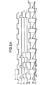
- FIGS. 5a and 5b show timing diagrams illustrating the state of the signals produced by the circuit of FIG. 4.
- FIG. 5a corresponds to the general case of operation
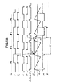
- FIG. 5b corresponds to the particular case where the voltage-delay converter does not can provide the delay requested for example when the delay of the HR signal on The H signal must be very weak or close to an entire period.
- the HR signal then no longer has a rising edge and the output of the monostable flip-flop 72 changes state.
- FIG. 5a there is shown successively the clock signal H, of period T, the transition signal TS, the signal V ⁇ indicating the phase difference between the transition signal TS and the clock signal HR, the signal V ⁇ o indicating a reference phase, the clock signal HR and
- the signals VD and VC applied respectively to the inverting and non-inverting inputs of comparator 56 (FIG. 4).
- the rising edges of the signal TS put the signals V ⁇ and V ⁇ o at the high level.
- the signal V ⁇ o falls after an adjustable fixed duration; in the figure, this duration is equal to T / 2.
- the signal V ⁇ falls on the rising edge of the clock signal HR. The state of the latter is equal to the sign of the difference VC-VD.
- the clock signal HR On the first two transitions of the TS signal, the clock signal HR has a delay of less than T / 2; the pulses of V ⁇ are therefore lower than those of V ⁇ 'which results in variations 80 and 82 of the signal VC. This delays the HR clock signal until it is offset by T / 2 from the TS transition signal.
- the symmetrical case of the previous one is represented where ⁇ is greater than ⁇ o .
- the level of the signal VC increases which advances the rising edges of the clock signal HR.
- the state of the various signals is such that the signal VC becomes greater than the peak value of the signal VD. Then the clock signal HR no longer switches and after a duration T1, slightly greater than T, the signal M goes high. This resets the signal VC to zero and changes the state of flip-flop 70, which has the effect of reversing the phase of the clock signal H 'controlling the sawtooth signal which is therefore advanced by half a period of the clock signal H. The signal M falls on the first next rising edge of the clock signal HR.
- the clock signal HR then evolves as in FIG. 5a so as to be shifted by T / 2 with the transition signal TS.
Landscapes
- Engineering & Computer Science (AREA)
- Computer Networks & Wireless Communication (AREA)
- Signal Processing (AREA)
- Stabilization Of Oscillater, Synchronisation, Frequency Synthesizers (AREA)
- Synchronisation In Digital Transmission Systems (AREA)
Applications Claiming Priority (2)
| Application Number | Priority Date | Filing Date | Title |
|---|---|---|---|
| FR8412675A FR2569070B1 (fr) | 1984-08-10 | 1984-08-10 | Procede et dispositif d'acquisition rapide du rythme et de la phase d'un signal numerique |
| FR8412675 | 1984-08-10 |
Publications (2)
| Publication Number | Publication Date |
|---|---|
| EP0174237A1 true EP0174237A1 (de) | 1986-03-12 |
| EP0174237B1 EP0174237B1 (de) | 1989-11-02 |
Family
ID=9306968
Family Applications (1)
| Application Number | Title | Priority Date | Filing Date |
|---|---|---|---|
| EP19850401586 Expired EP0174237B1 (de) | 1984-08-10 | 1985-08-02 | Einrichtung zum schnellen Erlangen des Taktes und der Phasen eines digitalen Signals |
Country Status (3)
| Country | Link |
|---|---|
| EP (1) | EP0174237B1 (de) |
| DE (1) | DE3574093D1 (de) |
| FR (1) | FR2569070B1 (de) |
Cited By (2)
| Publication number | Priority date | Publication date | Assignee | Title |
|---|---|---|---|---|
| FR2606568A1 (fr) * | 1986-11-06 | 1988-05-13 | Milon Jean | Procede et dispositif d'acquisition rapide du rythme et de la phase d'un signal numerique, utilisant une boucle a verrouillage de phase analogique et des sauts de phase |
| US9071921B2 (en) | 2009-12-23 | 2015-06-30 | Futurewei Technologies, Inc. | System and method for event driven operations in a communications system |
Citations (4)
| Publication number | Priority date | Publication date | Assignee | Title |
|---|---|---|---|---|
| DE2654927A1 (de) * | 1976-12-03 | 1978-06-08 | Siemens Ag | Schaltungsanordnung zur abtastung einseitig verzerrter fernschreibzeichen |
| US4229824A (en) * | 1978-07-21 | 1980-10-21 | Cubic Corporation | Method and apparatus for synchronizing electrical signals |
| US4335361A (en) * | 1977-09-01 | 1982-06-15 | Honeywell Inc. | Variable gain amplifier |
| EP0054322A1 (de) * | 1980-12-12 | 1982-06-23 | Philips Electronics Uk Limited | Phasenempfindlicher Detektor |
Family Cites Families (1)
| Publication number | Priority date | Publication date | Assignee | Title |
|---|---|---|---|---|
| JPS5949745B2 (ja) * | 1980-09-08 | 1984-12-04 | 富士通株式会社 | クロック選択方式 |
-
1984
- 1984-08-10 FR FR8412675A patent/FR2569070B1/fr not_active Expired - Lifetime
-
1985
- 1985-08-02 EP EP19850401586 patent/EP0174237B1/de not_active Expired
- 1985-08-02 DE DE8585401586T patent/DE3574093D1/de not_active Expired
Patent Citations (4)
| Publication number | Priority date | Publication date | Assignee | Title |
|---|---|---|---|---|
| DE2654927A1 (de) * | 1976-12-03 | 1978-06-08 | Siemens Ag | Schaltungsanordnung zur abtastung einseitig verzerrter fernschreibzeichen |
| US4335361A (en) * | 1977-09-01 | 1982-06-15 | Honeywell Inc. | Variable gain amplifier |
| US4229824A (en) * | 1978-07-21 | 1980-10-21 | Cubic Corporation | Method and apparatus for synchronizing electrical signals |
| EP0054322A1 (de) * | 1980-12-12 | 1982-06-23 | Philips Electronics Uk Limited | Phasenempfindlicher Detektor |
Non-Patent Citations (1)
| Title |
|---|
| PATENTS ABSTRACTS OF JAPAN, vol. 6, no. 119 (E-116) [997], 3 juillet 1982; & JP - A - 57 48 841 (FUJITSU K.K.) 20.03.1982 * |
Cited By (2)
| Publication number | Priority date | Publication date | Assignee | Title |
|---|---|---|---|---|
| FR2606568A1 (fr) * | 1986-11-06 | 1988-05-13 | Milon Jean | Procede et dispositif d'acquisition rapide du rythme et de la phase d'un signal numerique, utilisant une boucle a verrouillage de phase analogique et des sauts de phase |
| US9071921B2 (en) | 2009-12-23 | 2015-06-30 | Futurewei Technologies, Inc. | System and method for event driven operations in a communications system |
Also Published As
| Publication number | Publication date |
|---|---|
| FR2569070B1 (fr) | 1991-04-19 |
| FR2569070A1 (fr) | 1986-02-14 |
| DE3574093D1 (en) | 1989-12-07 |
| EP0174237B1 (de) | 1989-11-02 |
Similar Documents
| Publication | Publication Date | Title |
|---|---|---|
| EP0190730B1 (de) | Einrichtung zur Dreifachtaktverteilung, wobei jedes Taktsignal ein Synchronisationssignal enthält | |
| FR2473816A1 (fr) | Systeme a blocage de boucle | |
| FR2882871A1 (fr) | Oscillateur commande en tension a multiphase realignee et boucle a phase asservie associee | |
| FR2696299A1 (fr) | Circuit de synthétiseur de fréquence à boucle à verrouillage de phase. | |
| FR2787651A1 (fr) | Detecteur numerique de frequence de phase | |
| EP0564377B1 (de) | Frequenzregelschleife | |
| FR2526619A1 (fr) | Circuit de multiplication de la frequence de balayage | |
| EP0015014A1 (de) | Vorrichtung zur schnellen Synchronisierung eines Taktsignals | |
| EP0716501A1 (de) | Phasenvergleicher für ein digitales Signal und ein Taktsignal, und entsprechender Phasenregelkreis | |
| FR2677515A1 (fr) | Circuit diviseur de frequence. | |
| EP0267422B1 (de) | Verfahren und Einrichtung zur Synchronisationshilfe einer Phasenregelschleife | |
| EP0302562B1 (de) | Frequenz-Synthetisierer mit einer Abstimm-Anzeigeeinrichtung | |
| EP0174237B1 (de) | Einrichtung zum schnellen Erlangen des Taktes und der Phasen eines digitalen Signals | |
| EP0055670B1 (de) | Schaltung zur Regelung des Tastverhältnisses eines periodischen Impulssignals und 2n-Frequenzvervielfacher mit dieser Regelschaltung | |
| EP1101316B1 (de) | Verfahren zur taktrückgewinnung während der abtastung von digitalen signalen | |
| FR2567698A1 (fr) | Procede et montage pour detecter la difference de phase/frequence entre deux signaux d'entree numeriques et application | |
| EP0042641B1 (de) | Frequenzdemodulator mit einer Verzögerungsschaltung, wobei die Verzögerung von der empfangenen Frequenz abhängig ist | |
| FR2552955A1 (fr) | Procede de commande de la frequence d'un oscillateur et circuit de commande a boucle d'asservissement de phase | |
| FR2816075A1 (fr) | Generateur ameliore pour la production de signaux d'horloge | |
| EP0541408B1 (de) | Verfahren und Einrichtung zum Steuern der Wirkungsweise eines digitalen Phasenregelkreises | |
| FR2573592A1 (fr) | Circuit oscillateur asservi en phase a un signal de frequence predeterminee | |
| FR2624673A1 (fr) | Oscillateur a commande numerique, utilisant un element commutable, application a la realisation de dispositifs de recuperation du rythme et de la phase d'un signal numerique | |
| EP0092879A2 (de) | Bitsynchronisiereinrichtung für Modulator-Demodulator oder Empfänger von Datenübertragung | |
| FR2606568A1 (fr) | Procede et dispositif d'acquisition rapide du rythme et de la phase d'un signal numerique, utilisant une boucle a verrouillage de phase analogique et des sauts de phase | |
| EP0868030B1 (de) | Phasenregelkreis mit Phasenregelhilfsschaltung |
Legal Events
| Date | Code | Title | Description |
|---|---|---|---|
| PUAI | Public reference made under article 153(3) epc to a published international application that has entered the european phase |
Free format text: ORIGINAL CODE: 0009012 |
|
| AK | Designated contracting states |
Kind code of ref document: A1 Designated state(s): DE GB NL |
|
| 17P | Request for examination filed |
Effective date: 19860816 |
|
| 17Q | First examination report despatched |
Effective date: 19880210 |
|
| GRAA | (expected) grant |
Free format text: ORIGINAL CODE: 0009210 |
|
| AK | Designated contracting states |
Kind code of ref document: B1 Designated state(s): DE GB NL |
|
| REF | Corresponds to: |
Ref document number: 3574093 Country of ref document: DE Date of ref document: 19891207 |
|
| GBT | Gb: translation of ep patent filed (gb section 77(6)(a)/1977) | ||
| PLBE | No opposition filed within time limit |
Free format text: ORIGINAL CODE: 0009261 |
|
| STAA | Information on the status of an ep patent application or granted ep patent |
Free format text: STATUS: NO OPPOSITION FILED WITHIN TIME LIMIT |
|
| 26N | No opposition filed | ||
| PGFP | Annual fee paid to national office [announced via postgrant information from national office to epo] |
Ref country code: GB Payment date: 19920728 Year of fee payment: 8 |
|
| PGFP | Annual fee paid to national office [announced via postgrant information from national office to epo] |
Ref country code: DE Payment date: 19920731 Year of fee payment: 8 |
|
| PGFP | Annual fee paid to national office [announced via postgrant information from national office to epo] |
Ref country code: NL Payment date: 19920831 Year of fee payment: 8 |
|
| PG25 | Lapsed in a contracting state [announced via postgrant information from national office to epo] |
Ref country code: GB Effective date: 19930802 |
|
| PG25 | Lapsed in a contracting state [announced via postgrant information from national office to epo] |
Ref country code: NL Effective date: 19940301 |
|
| GBPC | Gb: european patent ceased through non-payment of renewal fee |
Effective date: 19930802 |
|
| NLV4 | Nl: lapsed or anulled due to non-payment of the annual fee | ||
| PG25 | Lapsed in a contracting state [announced via postgrant information from national office to epo] |
Ref country code: DE Effective date: 19940503 |