EP0174506A2 - Capteur à fibres optiques pourvu d'une substance fluorescente - Google Patents
Capteur à fibres optiques pourvu d'une substance fluorescente Download PDFInfo
- Publication number
- EP0174506A2 EP0174506A2 EP85110082A EP85110082A EP0174506A2 EP 0174506 A2 EP0174506 A2 EP 0174506A2 EP 85110082 A EP85110082 A EP 85110082A EP 85110082 A EP85110082 A EP 85110082A EP 0174506 A2 EP0174506 A2 EP 0174506A2
- Authority
- EP
- European Patent Office
- Prior art keywords
- sensor according
- optic sensor
- voltage
- frequency
- fluorescence
- Prior art date
- Legal status (The legal status is an assumption and is not a legal conclusion. Google has not performed a legal analysis and makes no representation as to the accuracy of the status listed.)
- Granted
Links
- 239000000126 substance Substances 0.000 title claims abstract description 13
- 230000005855 radiation Effects 0.000 claims abstract description 35
- 230000005284 excitation Effects 0.000 claims abstract description 15
- 230000010355 oscillation Effects 0.000 claims abstract description 9
- 239000000835 fiber Substances 0.000 claims description 8
- 238000012937 correction Methods 0.000 claims description 6
- LOSYLUVSUPZXRV-UHFFFAOYSA-N B([O-])([O-])[O-].[Cr+3].[Al+3].[Lu+3].B([O-])([O-])[O-].B([O-])([O-])[O-] Chemical compound B([O-])([O-])[O-].[Cr+3].[Al+3].[Lu+3].B([O-])([O-])[O-].B([O-])([O-])[O-] LOSYLUVSUPZXRV-UHFFFAOYSA-N 0.000 claims description 3
- 239000011651 chromium Substances 0.000 claims 3
- 229910018072 Al 2 O 3 Inorganic materials 0.000 claims 1
- YPDOSCDKGDKCLX-UHFFFAOYSA-N B([O-])([O-])[O-].[Al+3].[Nd+3].B([O-])([O-])[O-] Chemical compound B([O-])([O-])[O-].[Al+3].[Nd+3].B([O-])([O-])[O-] YPDOSCDKGDKCLX-UHFFFAOYSA-N 0.000 claims 1
- 229910052779 Neodymium Inorganic materials 0.000 claims 1
- JNDMLEXHDPKVFC-UHFFFAOYSA-N aluminum;oxygen(2-);yttrium(3+) Chemical compound [O-2].[O-2].[O-2].[Al+3].[Y+3] JNDMLEXHDPKVFC-UHFFFAOYSA-N 0.000 claims 1
- OMZWVEWXCVONJK-UHFFFAOYSA-I lithium potassium neodymium(3+) pentafluoride Chemical compound [F-].[Li+].[K+].[Nd+3].[F-].[F-].[F-].[F-] OMZWVEWXCVONJK-UHFFFAOYSA-I 0.000 claims 1
- QEFYFXOXNSNQGX-UHFFFAOYSA-N neodymium atom Chemical compound [Nd] QEFYFXOXNSNQGX-UHFFFAOYSA-N 0.000 claims 1
- LFXISEXWRHFVGQ-UHFFFAOYSA-H neodymium(3+) [oxido-[oxido(phosphonatooxy)phosphoryl]oxyphosphoryl] phosphate Chemical compound [O-]P([O-])(=O)OP(=O)([O-])OP(=O)([O-])OP(=O)([O-])[O-].[Nd+3].[Nd+3] LFXISEXWRHFVGQ-UHFFFAOYSA-H 0.000 claims 1
- 239000010979 ruby Substances 0.000 claims 1
- 229910001750 ruby Inorganic materials 0.000 claims 1
- 229910019901 yttrium aluminum garnet Inorganic materials 0.000 claims 1
- 238000005259 measurement Methods 0.000 abstract description 3
- 238000010586 diagram Methods 0.000 description 18
- 230000008859 change Effects 0.000 description 8
- 230000003287 optical effect Effects 0.000 description 7
- 238000005516 engineering process Methods 0.000 description 6
- 230000001419 dependent effect Effects 0.000 description 5
- 230000008878 coupling Effects 0.000 description 4
- 238000010168 coupling process Methods 0.000 description 4
- 238000005859 coupling reaction Methods 0.000 description 4
- 230000010354 integration Effects 0.000 description 4
- 239000013307 optical fiber Substances 0.000 description 4
- 230000004044 response Effects 0.000 description 4
- 230000003321 amplification Effects 0.000 description 3
- 238000003199 nucleic acid amplification method Methods 0.000 description 3
- 239000013078 crystal Substances 0.000 description 2
- 230000009467 reduction Effects 0.000 description 2
- 238000012935 Averaging Methods 0.000 description 1
- 238000009529 body temperature measurement Methods 0.000 description 1
- 238000005352 clarification Methods 0.000 description 1
- 238000010276 construction Methods 0.000 description 1
- 239000006185 dispersion Substances 0.000 description 1
- 230000005672 electromagnetic field Effects 0.000 description 1
- -1 lutetium aluminum chromium Chemical compound 0.000 description 1
- 238000000034 method Methods 0.000 description 1
- 230000008569 process Effects 0.000 description 1
- 238000012545 processing Methods 0.000 description 1
- 230000035945 sensitivity Effects 0.000 description 1
- 239000007787 solid Substances 0.000 description 1
- 230000001629 suppression Effects 0.000 description 1
- 230000001360 synchronised effect Effects 0.000 description 1
- 230000002123 temporal effect Effects 0.000 description 1
Images


Classifications
-
- G—PHYSICS
- G01—MEASURING; TESTING
- G01D—MEASURING NOT SPECIALLY ADAPTED FOR A SPECIFIC VARIABLE; ARRANGEMENTS FOR MEASURING TWO OR MORE VARIABLES NOT COVERED IN A SINGLE OTHER SUBCLASS; TARIFF METERING APPARATUS; MEASURING OR TESTING NOT OTHERWISE PROVIDED FOR
- G01D5/00—Mechanical means for transferring the output of a sensing member; Means for converting the output of a sensing member to another variable where the form or nature of the sensing member does not constrain the means for converting; Transducers not specially adapted for a specific variable
- G01D5/26—Mechanical means for transferring the output of a sensing member; Means for converting the output of a sensing member to another variable where the form or nature of the sensing member does not constrain the means for converting; Transducers not specially adapted for a specific variable characterised by optical transfer means, i.e. using infrared, visible, or ultraviolet light
- G01D5/268—Mechanical means for transferring the output of a sensing member; Means for converting the output of a sensing member to another variable where the form or nature of the sensing member does not constrain the means for converting; Transducers not specially adapted for a specific variable characterised by optical transfer means, i.e. using infrared, visible, or ultraviolet light using optical fibres
-
- G—PHYSICS
- G01—MEASURING; TESTING
- G01K—MEASURING TEMPERATURE; MEASURING QUANTITY OF HEAT; THERMALLY-SENSITIVE ELEMENTS NOT OTHERWISE PROVIDED FOR
- G01K11/00—Measuring temperature based upon physical or chemical changes not covered by groups G01K3/00, G01K5/00, G01K7/00 or G01K9/00
- G01K11/32—Measuring temperature based upon physical or chemical changes not covered by groups G01K3/00, G01K5/00, G01K7/00 or G01K9/00 using changes in transmittance, scattering or luminescence in optical fibres
- G01K11/3206—Measuring temperature based upon physical or chemical changes not covered by groups G01K3/00, G01K5/00, G01K7/00 or G01K9/00 using changes in transmittance, scattering or luminescence in optical fibres at discrete locations in the fibre, e.g. using Bragg scattering
- G01K11/3213—Measuring temperature based upon physical or chemical changes not covered by groups G01K3/00, G01K5/00, G01K7/00 or G01K9/00 using changes in transmittance, scattering or luminescence in optical fibres at discrete locations in the fibre, e.g. using Bragg scattering using changes in luminescence, e.g. at the distal end of the fibres
Definitions
- the present invention relates to a fiber-optic sensor with a fluorescent substance whose fluorescence decay time depends on a physical variable, in which the fluorescent radiation is fed back to the excitation radiation in an oscillation circuit and the frequency of the oscillation circuit is therefore a measure of the physical quantity.
- Such a fiber optic sensor is known from DE-OS 32 02 089 for temperature measurements.
- a fluorescent substance is excited by a sinusoidally modulated emitter and the signal obtained from the time-delayed fluorescent light is fed back to the control of the modulator via a timing element.
- the frequency which arises in the self-exciting oscillation circuit depends on the fluorescence decay duration and thus on all physical quantities which influence it.
- the temperature to be measured is converted into the modulation frequency. This can be easily and precisely transferred over long distances.
- the excitation radiation being supplied to the measuring location and the fluorescent tube being removed from the measuring location via one (or two) optical fibers, use in high and low frequency alternating electromagnetic fields and at high electrical potentials is possible without any problems.
- the present invention is therefore based on the object of providing a fiber-optic sensor with a fluorescent substance which is distinguished by low noise, high sensitivity and great accuracy even over long periods and with changing ambient temperatures.
- the object is achieved according to the invention in that an oscillator is provided for the feedback of the fluorescence signal, for the control of which means are provided for evaluating the decay time of the fluorescence signal.
- decay time fluorescence time constant
- the noise at the DC voltage for the oscillator can e.g. can be suppressed by an RC element as much as the desired response behavior of the sensor allows. If the fluorescence signal is evaluated in digital technology, the noise can be suppressed to the same extent by appropriately averaging the values.
- the control for the oscillator can be obtained directly from the amplitude of the alternating voltage component of the fluorescence signal, since this is the smaller the greater the ratio of the fluorescence decay duration to the period duration Is excitation radiation.
- the relative change in frequency is therefore equal to the relative change in the fluorescence decay time if the fluorescence intensity is independent of the temperature, as is the case, for example, with lutetium aluminum chromium borate.
- a control of the oscillator is controlled by a dose-controlled rectifier, with which a part of the fluorescence signal is evaluated, and an integrator, with which this part of the fluorescence signal is integrated.
- a voltage-controlled oscillator is expediently used and a sample and hold amplifier (sample and hold circuit) is provided between it and the integrator output.
- the oscillator does not generate the modulation frequency itself, but a multiple thereof. Both the signal for the modulation and the clocked signal for the phase-controlled rectification are obtained from the oscillator frequency by reduction. Since the reduction is a pure payment process, the relative temporal position of the signal for the phase-controlled rectification to the signal for the modulation of the light source is not influenced by the temperature of electronic components.
- the radiation which stimulates the fluorescence takes on only two fixed values in alternation with the modulation frequency (modulation with a rectangular shape in time).
- the characteristic curve of the radiator thus has no influence and no special amplitude control is necessary.
- the scattered light that occurs in the optical part of the sensor becomes electronic Part taken into account by an (additional) control circuit, which evaluates the fluorescence signal and generates a correction value for the fluorescence signal during the bright phase of the radiation source.
- a correction voltage is applied to the amplifier for the fluorescence signal. It is expedient to provide an asymmetrical rectifier and an integrator for generating the correction value.
- a sense and hold amplifier and an electronic switch are also advantageous.
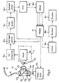
- 10 is a fluorescent substance, for example a lutetium aluminum chromium crystal, which is connected via the optical fiber 11 to the optical device 12, the latter having the task of emitting the radiation emanating from the radiation source 13a, for example an LED Converging lenses 12a and 12d and through the dichroic i table mirror 12c bring into the optical fiber 11, from which it is transmitted to the fluorescent substance 10.
- the fluorescence radiation produced there is transported back through the optical fiber 11 and brought from the optical device 12 via the converging lenses 12d and 12f and the dichroic mirror 12c to the receiver 14a, for example a photodiode.
- the filter 12b is transparent to the wavelength range necessary for the fluorescence excitation and the filter 12e is transparent to the wavelength range of the fluorescent radiation.
- Such a structure is known for example from DE-OS 32 02 089; it has only been described here for the sake of completeness.
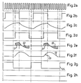
- the radiation source 13a is supplied with a rectangular voltage by the modulator 13b. This is shown in the time diagram in FIG. 2b.
- the voltage-controlled oscillator 16a does not use the modulation frequency of the radiation source, but a multiple, e.g. 14 times, generated. This output frequency of the oscillator 16a is shown in Figure 2a. In FIGS. 2, 3 and 5, all time diagrams have the same time axes.
- the output pulses of the oscillator are fed to a 4-bit synchronous counter 16b, the respective counter reading of which is evaluated in the form of a TTL binary number by the PROM 17, which supplies both the modulation pulses for the radiation source 13a and the clock pulses mentioned in the following text.
- the modulator 13b contains an operational amplifier, by means of which amplification and DC voltage addition the voltage levels for light and dark values of the radiation source can be set as desired. It is expedient to select the pulse duty factor for the modulation 1: 1, as shown in FIG. 2b.
- the fluorescence radiation generated in the fluorescent crystal 10 and detected by the receiver 14a is an e-function that begins to appear in time during the light phase and decays during the dark phase, as in the time diagram shown in Figure 2c.
- the low fluorescence signal is strongly amplified in amplifier 14b and then fed to active AC coupling 15a.
- the AC voltage is formed by an operational amplifier, which forms the difference between the incoming voltage and its DC voltage mean.
- the average DC voltage is obtained by supplying the output voltage of the operational amplifier to an integrator. Since a possible offset of the integrator causes errors, it is advisable to use a chopper-stabilized operational amplifier for the integrator.
- the phase-controlled half-period rectifier following the AC coupling 15a is controlled in such a way that it has the pass curve shown in the time diagram in FIG. 2d.
- He can e.g. can be realized by a combination of 2 MOSFET switches, which are controlled by two inverse TTL signals from the PROM 17 in such a way that the signal is passed on via a series switch for half the period and the following short-circuit switch is high-impedance during this time.
- the series switch is open and the short-circuit switch provides exactly 0 volts at the input of the following integrator 15c.
- the entire voltage curve at the input of the integrator 15c is shown in the time diagram in FIG. 2e.
- the integrator 15c is also chopper-stabilized to avoid offset errors; it therefore does not change its output signal during the half-periods in which the phase-dependent rectifier 15b is closed.
- the areas 21 and 22 in the time diagram m of FIG. 2e are of the same size, therefore the output voltage at the integrator 15c, which is shown in FIG. 2f, returns to the same value at the end of the opening time of the phase-dependent rectifier as before this time.
- the integrator 15c receives no signal and does not change its output signal due to its freedom from offset errors.
- the output signal is passed on to the sample and hold circuit 15d via a further MOSFET switch.
- the clock signal provided for this and shown in the time diagram in FIG. 2g becomes flat if generated in the PROM 17 from the frequency of the voltage controlled oscillator 16a.
- the output signal of the integrator 15c is stored in the sample and hold amplifier 15d during the next integration, designated 23 in FIG. 2f, so that it is available as a control voltage for the voltage-controlled oscillator 16a until a new integration result is available at time 24.
- the timing diagram of Figure 2h shows the control voltage for the voltage controlled oscillator 16a in the steady state, i.e. at constant temperature. In this case the control voltage is a constant DC voltage.
- FIG. 3 shows the time diagrams e to h of FIG. 2 for the case of a temperature change, which took place immediately before the start of the time diagrams for the purpose of the simplest possible representation as a temperature jump.
- 3 shows the voltage profile at the input of the integrator 15c.
- the fluorescence decay time has changed and the area labeled 30 is not as large as the area labeled 31. Since the entire measuring arrangement has a response time, the area 32 is not yet the same size as the area 33.
- the constant frequency in the steady state is characterized in that the period of the modulation of the excitation radiation in a certain ratio x to the fluorescence decay time.
- the PROM 17 is connected to the electronic counter 18a.
- the frequency values are converted into the measured values of the fluorescent substance 10, e.g. the computer 18b and the output of the measured values can e.g. with a printer 18c, a pen or a display.
- the frequency of the optical-electrical oscillation circuit is in the range of 220 to 1200 Hz for a temperature range of -30 to + 150 ° C and accordingly the frequency of the voltage-controlled oscillator 16a in the range of 3080 to 16800 Hz.
- the scattered light occurring in the optical part of the sensor is electrically compensated.
- This scattered light arises from the fact that the radiation source 13a also emits radiation in the wavelength range of the fluorescent light, a small part of it is passed through the filter 12b and is reflected at various interfaces of the optical parts, so that it likewise falls on the receiver 14a.
- excitation radiation is also reflected at the interfaces of the optical parts and is transmitted to a small extent through the filter 12e.
- the volume dispersion of the optical parts also plays a role. Overall, this creates a small amount of scattered light, but this cannot be disregarded in the case of very high demands on the measuring accuracy of the sensor.
- FIG. 5b shows the modulation signal for the radiation source 13a. During the bright phases of the radiation source, a small proportion of scattered light is generated, which changes the fluorescence signal during this time as shown by the dotted curve in FIG. 5c. The influence is exaggerated for clarification; if the filters 12b and 12f have good properties, it is of the order of 1%.
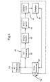
- the jumps in the fluorescence signal, designated 50 at the beginning and end of the light phases in FIG. 5, are therefore due to scattered light. They can be used directly for a compensation of the scattered light, in that a correction voltage is supplied to the differential amplifier 41 by a control circuit during the bright phases, which is so large that no jumps occur. Particularly good consideration of the stray light is obtained by the construction of the control circuit 40 described below.
- the automatic electrical compensation of the scattered light takes place in the following way:
- the output signal of the differential amplifier 41 is additionally fed to a second rectifier 43, the control of which is shown in FIG. 5d is in phase with the modulation of the radiation source (FIG. 5b).
- a DC coupling 42 is necessary.
- the gain in the second half-period is changed by a factor of 3.35 in accordance with the above information.
- the areas 51 and 53 are therefore of the same size if there is no stray light.
- the output voltage of the rectifier 43 is fed to the integrator 44, the output voltage of which is shown in FIG. 5f.
- the solid curve applies to the absence of scattered light, with the output voltage being zero at the end of the second half-period due to the equality of surfaces 51 and 53. If stray light is present, the dotted curve applies; in this case there is an output voltage at the end of the second half period.
- FIG. 5h shows the output voltage of the sample and hold amplifier 45, which is passed on to the differential amplifier 41 as a compensation voltage by the electronic switch 46 only during the first half period.
- the differential amplifier 41 receives no compensation voltage. As soon as stray light occurs, the compensation voltage changes until the surfaces 51 and 53 are the same again. The hatched areas thus apply to both stray light and electrically compensated stray light, in the latter case a compensation voltage is present which is changed when the stray light changes.
- a digitally controlled oscillator is expediently used. This can be done in such a way that the oscillator is operated at a fixed frequency which is so high that the excitation frequency can be obtained from it by subdivision with sufficient resolution. With an excitation frequency of approx. 1 kHz, a frequency of 50 MHz is sufficient for this.
Landscapes
- Physics & Mathematics (AREA)
- General Physics & Mathematics (AREA)
- Investigating, Analyzing Materials By Fluorescence Or Luminescence (AREA)
Applications Claiming Priority (2)
| Application Number | Priority Date | Filing Date | Title |
|---|---|---|---|
| DE19843431997 DE3431997A1 (de) | 1984-08-31 | 1984-08-31 | Faseroptischer sensor mit einer fluoreszierenden substanz |
| DE3431997 | 1984-08-31 |
Related Child Applications (2)
| Application Number | Title | Priority Date | Filing Date |
|---|---|---|---|
| EP19900115448 Division EP0402962A3 (fr) | 1984-08-31 | 1985-08-12 | Capteur à fibres optiques pourvu d'une substance fluorescente |
| EP90115448.4 Division-Into | 1985-08-12 |
Publications (3)
| Publication Number | Publication Date |
|---|---|
| EP0174506A2 true EP0174506A2 (fr) | 1986-03-19 |
| EP0174506A3 EP0174506A3 (en) | 1988-04-06 |
| EP0174506B1 EP0174506B1 (fr) | 1991-10-23 |
Family
ID=6244328
Family Applications (2)
| Application Number | Title | Priority Date | Filing Date |
|---|---|---|---|
| EP85110082A Expired - Lifetime EP0174506B1 (fr) | 1984-08-31 | 1985-08-12 | Capteur à fibres optiques pourvu d'une substance fluorescente |
| EP19900115448 Withdrawn EP0402962A3 (fr) | 1984-08-31 | 1985-08-12 | Capteur à fibres optiques pourvu d'une substance fluorescente |
Family Applications After (1)
| Application Number | Title | Priority Date | Filing Date |
|---|---|---|---|
| EP19900115448 Withdrawn EP0402962A3 (fr) | 1984-08-31 | 1985-08-12 | Capteur à fibres optiques pourvu d'une substance fluorescente |
Country Status (2)
| Country | Link |
|---|---|
| EP (2) | EP0174506B1 (fr) |
| DE (2) | DE3431997A1 (fr) |
Cited By (6)
| Publication number | Priority date | Publication date | Assignee | Title |
|---|---|---|---|---|
| EP0238856A1 (fr) * | 1986-02-21 | 1987-09-30 | Degussa Aktiengesellschaft | Procédé et dispositif pour mesurer la période de diminution de fluorescence d'une substance fluorescente |
| EP0283289A3 (fr) * | 1987-03-20 | 1989-08-16 | C.R. Bard, Inc. | Appareil d'excitation et de détection pour capteur à distance connecté par fibre optique |
| EP0379941A3 (fr) * | 1989-01-24 | 1991-05-08 | Tacan Corporation | Matériau de fluorescence |
| US5107445A (en) * | 1990-12-04 | 1992-04-21 | Luxtron Corporation | Modular luminescence-based measuring system using fast digital signal processing |
| EP0553261A4 (en) * | 1990-10-18 | 1993-10-20 | Rosemount Inc. | Trd temperature sensor and electronics |
| WO1999009382A1 (fr) * | 1997-08-13 | 1999-02-25 | De La Rue International Limited | Procedes et dispositif de detection |
Families Citing this family (4)
| Publication number | Priority date | Publication date | Assignee | Title |
|---|---|---|---|---|
| US4834497A (en) * | 1987-02-27 | 1989-05-30 | The United States Of American As Represented By The United States Department Of Energy | Fiber optic fluid detector |
| DE3709065A1 (de) * | 1987-03-19 | 1988-09-29 | Max Planck Gesellschaft | Verfahren und einrichtung zur beruehrungsfreien messung der temperaturverteilung in einem messvolumen |
| DE9004633U1 (de) * | 1990-04-25 | 1990-06-28 | Fa. Carl Zeiss, 7920 Heidenheim | Optische Weiche |
| DE10253821B3 (de) * | 2002-11-18 | 2004-07-22 | RUBITEC Gesellschaft für Innovation und Technologie der Ruhr-Universität Bochum mbH | Messvorrichtung |
Family Cites Families (1)
| Publication number | Priority date | Publication date | Assignee | Title |
|---|---|---|---|---|
| DE3202089C2 (de) * | 1982-01-23 | 1985-01-17 | Fa. Carl Zeiss, 7920 Heidenheim | Faseroptischer Temperatursensor |
-
1984
- 1984-08-31 DE DE19843431997 patent/DE3431997A1/de not_active Withdrawn
-
1985
- 1985-08-12 EP EP85110082A patent/EP0174506B1/fr not_active Expired - Lifetime
- 1985-08-12 DE DE8585110082T patent/DE3584492D1/de not_active Expired - Lifetime
- 1985-08-12 EP EP19900115448 patent/EP0402962A3/fr not_active Withdrawn
Cited By (8)
| Publication number | Priority date | Publication date | Assignee | Title |
|---|---|---|---|---|
| EP0238856A1 (fr) * | 1986-02-21 | 1987-09-30 | Degussa Aktiengesellschaft | Procédé et dispositif pour mesurer la période de diminution de fluorescence d'une substance fluorescente |
| EP0283289A3 (fr) * | 1987-03-20 | 1989-08-16 | C.R. Bard, Inc. | Appareil d'excitation et de détection pour capteur à distance connecté par fibre optique |
| EP0379941A3 (fr) * | 1989-01-24 | 1991-05-08 | Tacan Corporation | Matériau de fluorescence |
| EP0553261A4 (en) * | 1990-10-18 | 1993-10-20 | Rosemount Inc. | Trd temperature sensor and electronics |
| US5107445A (en) * | 1990-12-04 | 1992-04-21 | Luxtron Corporation | Modular luminescence-based measuring system using fast digital signal processing |
| US5351268A (en) * | 1990-12-04 | 1994-09-27 | Luxtron Corporation | Modular luminescence-based measuring system using fast digital signal processing |
| WO1999009382A1 (fr) * | 1997-08-13 | 1999-02-25 | De La Rue International Limited | Procedes et dispositif de detection |
| US6024202A (en) * | 1997-08-13 | 2000-02-15 | De La Rue International Limited | Detector methods and apparatus |
Also Published As
| Publication number | Publication date |
|---|---|
| EP0174506B1 (fr) | 1991-10-23 |
| DE3584492D1 (de) | 1991-11-28 |
| EP0402962A3 (fr) | 1990-12-27 |
| EP0402962A2 (fr) | 1990-12-19 |
| EP0174506A3 (en) | 1988-04-06 |
| DE3431997A1 (de) | 1986-03-13 |
Similar Documents
| Publication | Publication Date | Title |
|---|---|---|
| EP0009220B1 (fr) | Système pour la transmission de signaux par une liaison optique | |
| DE2744845C3 (de) | Verfahren zur Kompensation der elektrochemischen Störgleichspannung bei der magnetisch-induktiven Durchflußmessung mit periodisch umgepoltem magnetischem Gleichfeld | |
| DE69228490T2 (de) | Vorspannungssteuerung und -verfahren fuer elektro-optische modulatoren | |
| EP0439011B1 (fr) | Télémètre | |
| DE4223337C2 (de) | Verfahren und Anordnung zur photothermischen Spektroskopie | |
| EP0238856B1 (fr) | Procédé et dispositif pour mesurer la période de diminution de fluorescence d'une substance fluorescente | |
| EP0174506B1 (fr) | Capteur à fibres optiques pourvu d'une substance fluorescente | |
| DE3326555A1 (de) | Messvorrichtung mit doppelbrechung | |
| EP0400197B1 (fr) | Procédé et dispositif pour la démodulation du signal de la vitesse angulaire d'un gyroscope à fibre optique | |
| DE3202089A1 (de) | Faseroptischer temperatursensor | |
| EP0050306A2 (fr) | Dispositif de mesure à fibres optiques | |
| DE3122168A1 (de) | Elektronischer wirkverbrauchszaehler | |
| DE3800265A1 (de) | Spannungs-frequenz-umsetzer und seine verwendung in einer lichtwellenleiter-uebertragungsanordnung | |
| DE3530011C3 (de) | Verfahren und Vorrichtung zur Unterdrückung des Einflusses von Störlicht bei einer Meßlichtschranke | |
| DE3410798C2 (de) | Elektromagnetischer Strömungsmesser | |
| DE69125254T2 (de) | Optischer Pulsoszillator und damit arbeitende Vorrichtung zur Lichtfrequenzmessung | |
| DE3443600C2 (fr) | ||
| EP0483501B1 (fr) | Interféromètre de sagnac à fibre optique pour la mesure de la vitesse de rotation | |
| DE69007668T2 (de) | Faseroptischer Kreisel. | |
| EP0250028B1 (fr) | Dispositif de montage pour la compensation de dérivés dépendants ou non de la température d'un capteur capacitif | |
| EP0280261A2 (fr) | Circuit pour la production d'un signal carré indépendant de la température à une grandeur mesurée | |
| DE4133131C2 (de) | Anordnung zum Bestimmen von die Lichtintensität beeinflussenden chemischen und/oder physikalischen Größen | |
| DE3928584C2 (fr) | ||
| DE3244010A1 (de) | Einrichtung zur messung der rotationsgeschwindigkeit | |
| WO1982004117A1 (fr) | Organe de mesure optique pour fils et cables |
Legal Events
| Date | Code | Title | Description |
|---|---|---|---|
| PUAI | Public reference made under article 153(3) epc to a published international application that has entered the european phase |
Free format text: ORIGINAL CODE: 0009012 |
|
| AK | Designated contracting states |
Kind code of ref document: A2 Designated state(s): DE FR GB IT SE |
|
| RAP1 | Party data changed (applicant data changed or rights of an application transferred) |
Owner name: CARL-ZEISS-STIFTUNG TRADING AS CARL ZEISS Owner name: FIRMA CARL ZEISS |
|
| PUAL | Search report despatched |
Free format text: ORIGINAL CODE: 0009013 |
|
| AK | Designated contracting states |
Kind code of ref document: A3 Designated state(s): DE FR GB IT SE |
|
| 17P | Request for examination filed |
Effective date: 19881004 |
|
| 17Q | First examination report despatched |
Effective date: 19891201 |
|
| ITF | It: translation for a ep patent filed | ||
| GRAA | (expected) grant |
Free format text: ORIGINAL CODE: 0009210 |
|
| AK | Designated contracting states |
Kind code of ref document: B1 Designated state(s): DE FR GB IT SE |
|
| XX | Miscellaneous (additional remarks) |
Free format text: TEILANMELDUNG 90115448.4 EINGEREICHT AM 12/08/85. |
|
| REF | Corresponds to: |
Ref document number: 3584492 Country of ref document: DE Date of ref document: 19911128 |
|
| ET | Fr: translation filed | ||
| GBT | Gb: translation of ep patent filed (gb section 77(6)(a)/1977) | ||
| PLBE | No opposition filed within time limit |
Free format text: ORIGINAL CODE: 0009261 |
|
| STAA | Information on the status of an ep patent application or granted ep patent |
Free format text: STATUS: NO OPPOSITION FILED WITHIN TIME LIMIT |
|
| 26N | No opposition filed | ||
| REG | Reference to a national code |
Ref country code: GB Ref legal event code: 732E |
|
| ITPR | It: changes in ownership of a european patent |
Owner name: CESSIONE;LUXTRON CORPORATION |
|
| PGFP | Annual fee paid to national office [announced via postgrant information from national office to epo] |
Ref country code: SE Payment date: 19940831 Year of fee payment: 10 |
|
| EAL | Se: european patent in force in sweden |
Ref document number: 85110082.6 |
|
| PG25 | Lapsed in a contracting state [announced via postgrant information from national office to epo] |
Ref country code: SE Effective date: 19950813 |
|
| EUG | Se: european patent has lapsed |
Ref document number: 85110082.6 |
|
| REG | Reference to a national code |
Ref country code: GB Ref legal event code: IF02 |
|
| PGFP | Annual fee paid to national office [announced via postgrant information from national office to epo] |
Ref country code: FR Payment date: 20040810 Year of fee payment: 20 |
|
| PGFP | Annual fee paid to national office [announced via postgrant information from national office to epo] |
Ref country code: GB Payment date: 20040818 Year of fee payment: 20 |
|
| PGFP | Annual fee paid to national office [announced via postgrant information from national office to epo] |
Ref country code: DE Payment date: 20040819 Year of fee payment: 20 |
|
| PG25 | Lapsed in a contracting state [announced via postgrant information from national office to epo] |
Ref country code: GB Free format text: LAPSE BECAUSE OF EXPIRATION OF PROTECTION Effective date: 20050811 |
|
| REG | Reference to a national code |
Ref country code: GB Ref legal event code: PE20 |