EP0174880A1 - Schaltungsanordnung zum Feststellen der Übergänge eines Datensignals in Bezug auf ein Taktsignal und diese Anordnung enthaltende Synchronisationseinrichtung - Google Patents
Schaltungsanordnung zum Feststellen der Übergänge eines Datensignals in Bezug auf ein Taktsignal und diese Anordnung enthaltende Synchronisationseinrichtung Download PDFInfo
- Publication number
- EP0174880A1 EP0174880A1 EP85401450A EP85401450A EP0174880A1 EP 0174880 A1 EP0174880 A1 EP 0174880A1 EP 85401450 A EP85401450 A EP 85401450A EP 85401450 A EP85401450 A EP 85401450A EP 0174880 A1 EP0174880 A1 EP 0174880A1
- Authority
- EP
- European Patent Office
- Prior art keywords
- signal
- clock
- data
- flip
- data signal
- Prior art date
- Legal status (The legal status is an assumption and is not a legal conclusion. Google has not performed a legal analysis and makes no representation as to the accuracy of the status listed.)
- Granted
Links
- 230000007704 transition Effects 0.000 title claims abstract description 21
- 230000004807 localization Effects 0.000 title description 3
- 230000001360 synchronised effect Effects 0.000 claims abstract description 8
- 238000009432 framing Methods 0.000 claims description 12
- 238000010200 validation analysis Methods 0.000 claims description 5
- 238000005070 sampling Methods 0.000 description 15
- 238000010586 diagram Methods 0.000 description 9
- 238000001514 detection method Methods 0.000 description 4
- 238000013459 approach Methods 0.000 description 3
- 230000010363 phase shift Effects 0.000 description 3
- 230000033764 rhythmic process Effects 0.000 description 3
- 230000003111 delayed effect Effects 0.000 description 2
- 230000000694 effects Effects 0.000 description 2
- 238000011144 upstream manufacturing Methods 0.000 description 2
- 239000008186 active pharmaceutical agent Substances 0.000 description 1
- 230000005540 biological transmission Effects 0.000 description 1
- 238000010276 construction Methods 0.000 description 1
- 230000001934 delay Effects 0.000 description 1
- 238000000034 method Methods 0.000 description 1
- 238000000638 solvent extraction Methods 0.000 description 1
Images
Classifications
-
- H—ELECTRICITY
- H04—ELECTRIC COMMUNICATION TECHNIQUE
- H04L—TRANSMISSION OF DIGITAL INFORMATION, e.g. TELEGRAPHIC COMMUNICATION
- H04L7/00—Arrangements for synchronising receiver with transmitter
- H04L7/02—Speed or phase control by the received code signals, the signals containing no special synchronisation information
- H04L7/033—Speed or phase control by the received code signals, the signals containing no special synchronisation information using the transitions of the received signal to control the phase of the synchronising-signal-generating means, e.g. using a phase-locked loop
-
- H—ELECTRICITY
- H04—ELECTRIC COMMUNICATION TECHNIQUE
- H04L—TRANSMISSION OF DIGITAL INFORMATION, e.g. TELEGRAPHIC COMMUNICATION
- H04L7/00—Arrangements for synchronising receiver with transmitter
- H04L7/02—Speed or phase control by the received code signals, the signals containing no special synchronisation information
- H04L7/033—Speed or phase control by the received code signals, the signals containing no special synchronisation information using the transitions of the received signal to control the phase of the synchronising-signal-generating means, e.g. using a phase-locked loop
- H04L7/0337—Selecting between two or more discretely delayed clocks or selecting between two or more discretely delayed received code signals
Definitions
- the subject of the invention is a device for locating the transitions of a data signal transmitted in digital form with respect to the successive edges of a synchronous or plesiochronous local clock signal of the data signal. It is in particular usable in a mechanism making it possible to frame the local clock signal with respect to a data signal initially presenting a random phase relation with the clock signal, in order to allow the capture of the data by sampling in a centered range in the interval of time of presence of the data and of duration much shorter than that of this interval.
- document EP-A-21 942 describes a framing device for a data transmission system in the form of sequences of limited length, each comprising an identifiable header. The framing is carried out on a local plesiochronous clock. Because of the limited length of the sequences, it avoids excessive drift compared to the framing, which is carried out once and for all at the start of each sequence.
- the invention aims in particular to provide a device implementing the detection of transitions of the current part of the data signal, device adaptable to any digital signal.
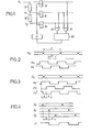
- the invention proposes in particular a device which comprises at least three flip-flops each of which has a validation input which receives the local clock signal and a data input which receives the data signal with a time offset determined by delay means and different for each flip-flop, as well as logic means connected to the output of the flip-flops and designed to generate, as a function of a predetermined criterion, a signal representative of the phase relationship between the clock signal and the data signal.
- the time shifts can be carried out by taking the data signal from several successive locations of delay means; but we can arrive at an equivalent result, although in a slightly more complex way, by realizing the time shift by action no longer on the data signal, but on the clock signal.
- the mechanism thus proposed makes it possible to control the instant of sampling of the data signal by the clock and to maintain this instant, by judicious servoing, as far as possible from the data transition. This eliminates any sampling uncertainty, the valid information being obtained at the output of the center flip-flop 12.
- the servo should allow, by action on a variable delay line, to obtain a correct framing between these signals.
- the data and clock signals will be plesiochronous with one another; the servo then acts, by command on the frequency of the clock oscillator, so that there is identity between the global rhythm of the clock and the rhythm of the data. The two approaches will be described successively.
- the sampling must be carried out on validity ranges 2v centered with respect to the time intervals of presence of the data ( Figure 2).
- the clock signal Ho having any phase relative to the data signal Do, it is necessary to bring and maintain the clock fronts in the ranges of width 2v by phase shift of one of the signals, for example by phase shift of the signal clock to bring it in Hv.
- the principle implemented by the invention involves creating, from the clock signal Ho, at least two signals Ho + and Ho- shifted by + ⁇ and -6 respectively with ⁇ ⁇ T ( Figure 3). In practice, it is the same to create, from the data signal, two other signals D 1 and D 2 offset respectively by +6 and +26 ( Figure 4).
- the device comprises at least three flip-flops (10, 12, 14). Each flip-flop receives the clock signal H on a validation input and receives the data signal with a time offset with respect to the clock, determined by delay means 18 and 20, different for each flip-flop.
- the received signal D O thus gives rise to the signals D 1 and D 2 .
- Logic means comprising in FIG. 1 a combinatorial logic 30 and EXCLUSIVE OR gates 32, 34, control the clock.
- the phase control mechanism can be implemented each time there is a data signal accompanied by a synchronous clock signal of the latter but not having with it a known phase relationship. These two signals can moreover be assigned, with respect to each other, a time jitter which must be taken into account in the construction of the system.
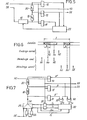
- the general principle is given in Figure 5.
- the approach consists in adopting a common value ⁇ (or values ⁇ 1 and ⁇ 2 ) less than T / 2 and shifting the clock signal and the data signal relative to each other so that the three samplings Ho, Ho- and Ho + enter an identical value in functionally stationary. Compliance with this condition guarantees that the Ho fronts are not close to a data transition. If this condition is not observed, the clock signal must be shifted downstream if the sample taken from the Ho- transitions is different from the others, as shown in the second line of Figure 3, and Conversely.
- the maximum admissible jitter will therefore be the minimum of two values:
- the locator applying this approach can use either several data signals arising from each other and whose transitions are offset by ô, or clock signals arising from each other and offset by ((the signal not subject to offset remaining single and fixed).
- the first solution will be more generally more convenient to implement. It can in particular be incorporated into a cropping mechanism of the kind shown in FIG. 5.
- the mechanism of Figure 5 has two inputs DE and HE to which the data signal and a synchronous clock signal of the data signal are respectively applied.
- the location device comprises three flip-flops 10, 12 and 14.
- the validation input of each clock is connected to the HE input so as to directly receive the local clock signal.
- the HE input is also connected directly to the HS clock output terminal.
- the data signal arriving at the terminal DE crosses a delay line 16 programmable by jumps of amplitude k.
- the data signal at output DS will consist of the output of the center flip-flop 12.
- the number n of elementary steps provided by the delay line 16 must be such that one can always find a delay pk, with 0 ⁇ p ⁇ n, such that one can get out of a situation where the fronts of clock can be found in zone I or III. For this, it is necessary, in the case of a peak to peak jitter amplitude w that: which, in the optimal situation envisaged above in (3) results in:
- the delay line can then be constituted by a multiplexer 24 with three inputs associated with two elements 26 each providing a delay T / 3. Switching is controlled by a 2-bit register 28 which receives the clock signal on its validation input and signals Yo and Y1 coming from combinational logic 30 on its data inputs.
- Combinatorial logic 30 itself receives the output signals Zo and Z1 from register 28 and logic signals XO and X1 supplied by EXCLUSIVE OR gates 32 and 34.
- the two inputs of each of gates 32 and 34 are connected to the output of two successive flip-flops among flip-flops 10, 12 and 14.
- Combinatorial logic 30 allows an analysis by detecting the four possible combinations of signals Xo and X1, which correspond to the combinations of states of flip-flops 10, 12 and 14 given by the table:
- the truth table of the multiplexer 24 is: where a, b and c denote the inputs respectively connected to the data input DE, to the delayed input of T / 3, to the delayed input of 2T / 3.
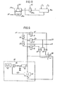
- a second embodiment of the invention must be implemented when the condition of synchronism between clock and data does not exist. Frequency alignment can then be done by slaving on the data transitions.
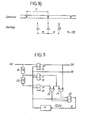
- a simple solution consists in using a generator capable of operating between two frequencies f1 and f2, one of which is for sure lower and the other for sure greater than the frequency of reception of the data signalDE. The direction of drift is reversed by switching from one clock rate to the other when the phase shift between the data signal and the sampling clock signal exceeds a determined threshold.
- the frequency generator 40 comprises a clock 42 which supplies a fixed frequency fo / N such that the frequencies fo (N-1) / N and (N + 1) fo / N are respectively lower and higher than the arrival frequency of the input data DE.
- the flip-flop 38 controls the division ratio of the loop of the frequency generator 40. For this, it attacks a programmable divider 44 whose division ratio is N-1 when the signal received from the flip-flop 38 is 0, N + 1 when the signal received is at logic level 1.
- the loop in which the divider 44 is placed comprises an EXCLUSIVE OR gate 46, used as a phase comparator, which receives, on one input, the output signal of the clock 42, on the other, the output signal of the divider .
- the EXCLUSIVE OR gate 46 attacks, via an RC filter, the frequency setting input of an oscillator 46 which supplies the clock signal H to the location device and to the divider 44. It can be seen that the flip-flop 38 determines at any time which of the frequencies is the most suitable and selects the appropriate division ratio of the phase-locked loop. The selection is made according to the following table:
- the values of 6 (which sets the detection framing for signal framing) and of N (which determines how fine the framing of the data reception frequency is by the values which the local clock frequency can take) will be chosen. depending on the characteristics of the signal. In particular, the choice must take into account that a continuous drift occurs if the frequency of the data signal remains stable for a long period and can lead to sampling error.
Landscapes
- Engineering & Computer Science (AREA)
- Computer Networks & Wireless Communication (AREA)
- Signal Processing (AREA)
- Stabilization Of Oscillater, Synchronisation, Frequency Synthesizers (AREA)
- Synchronisation In Digital Transmission Systems (AREA)
Applications Claiming Priority (2)
| Application Number | Priority Date | Filing Date | Title |
|---|---|---|---|
| FR8411190 | 1984-07-13 | ||
| FR8411190A FR2567697B1 (fr) | 1984-07-13 | 1984-07-13 | Dispositif de localisation des transitions d'un signal de donnees par rapport a un signal d'horloge et mecanisme de cadrage comprenant un tel dispositif |
Publications (2)
| Publication Number | Publication Date |
|---|---|
| EP0174880A1 true EP0174880A1 (de) | 1986-03-19 |
| EP0174880B1 EP0174880B1 (de) | 1989-09-20 |
Family
ID=9306128
Family Applications (1)
| Application Number | Title | Priority Date | Filing Date |
|---|---|---|---|
| EP19850401450 Expired EP0174880B1 (de) | 1984-07-13 | 1985-07-15 | Schaltungsanordnung zum Feststellen der Übergänge eines Datensignals in Bezug auf ein Taktsignal und diese Anordnung enthaltende Synchronisationseinrichtung |
Country Status (3)
| Country | Link |
|---|---|
| EP (1) | EP0174880B1 (de) |
| DE (1) | DE3573203D1 (de) |
| FR (1) | FR2567697B1 (de) |
Cited By (4)
| Publication number | Priority date | Publication date | Assignee | Title |
|---|---|---|---|---|
| EP0280126A3 (en) * | 1987-02-21 | 1990-03-07 | Deutsche Thomson-Brandt Gmbh | Programmable frequency divider and method for generating a low-frequency signal from a high-frequency signal |
| WO1991003895A1 (en) * | 1989-09-11 | 1991-03-21 | Raynet Corporation | Clock recovery apparatus |
| EP1063809A3 (de) * | 1999-06-24 | 2003-04-23 | Nec Corporation | Verfahren und Vorrichtung zum Empfand von hochrätigen Daten |
| US7254205B2 (en) | 1999-08-13 | 2007-08-07 | Agere Systems Inc. | Signal processing method and apparatus for ensuring a desired relationship between signals |
Families Citing this family (1)
| Publication number | Priority date | Publication date | Assignee | Title |
|---|---|---|---|---|
| ATE128296T1 (de) * | 1990-03-26 | 1995-10-15 | Siemens Ag | Taktsynchronisationsschaltung. |
Citations (5)
| Publication number | Priority date | Publication date | Assignee | Title |
|---|---|---|---|---|
| US3908084A (en) * | 1974-10-07 | 1975-09-23 | Bell Telephone Labor Inc | High frequency character receiver |
| EP0023852A1 (de) * | 1979-07-27 | 1981-02-11 | Thomson-Csf | Verfahren und Vorrichtung zur Phasenregelung eines lokalen Taktgebers |
| WO1981001226A1 (en) * | 1979-10-29 | 1981-04-30 | Burroughs Corp | Self synchronizing clock derivation circuit for double frequency encoded digital data |
| US4400817A (en) * | 1980-12-30 | 1983-08-23 | Motorola, Inc. | Method and means of clock recovery in a received stream of digital data |
| EP0102598A1 (de) * | 1979-11-09 | 1984-03-14 | Siemens Nixdorf Informationssysteme Aktiengesellschaft | Vorrichtung zur Phasensynchronisierung |
-
1984
- 1984-07-13 FR FR8411190A patent/FR2567697B1/fr not_active Expired - Lifetime
-
1985
- 1985-07-15 EP EP19850401450 patent/EP0174880B1/de not_active Expired
- 1985-07-15 DE DE8585401450T patent/DE3573203D1/de not_active Expired
Patent Citations (5)
| Publication number | Priority date | Publication date | Assignee | Title |
|---|---|---|---|---|
| US3908084A (en) * | 1974-10-07 | 1975-09-23 | Bell Telephone Labor Inc | High frequency character receiver |
| EP0023852A1 (de) * | 1979-07-27 | 1981-02-11 | Thomson-Csf | Verfahren und Vorrichtung zur Phasenregelung eines lokalen Taktgebers |
| WO1981001226A1 (en) * | 1979-10-29 | 1981-04-30 | Burroughs Corp | Self synchronizing clock derivation circuit for double frequency encoded digital data |
| EP0102598A1 (de) * | 1979-11-09 | 1984-03-14 | Siemens Nixdorf Informationssysteme Aktiengesellschaft | Vorrichtung zur Phasensynchronisierung |
| US4400817A (en) * | 1980-12-30 | 1983-08-23 | Motorola, Inc. | Method and means of clock recovery in a received stream of digital data |
Non-Patent Citations (1)
| Title |
|---|
| IBM TECHNICAL DISCLOSURE BULLETIN, vol. 18, no. 10, mars 1976, pages 3334-3337, New York, US; W.C. LEUNG: "Digital phase-locked loop circuit" * |
Cited By (4)
| Publication number | Priority date | Publication date | Assignee | Title |
|---|---|---|---|---|
| EP0280126A3 (en) * | 1987-02-21 | 1990-03-07 | Deutsche Thomson-Brandt Gmbh | Programmable frequency divider and method for generating a low-frequency signal from a high-frequency signal |
| WO1991003895A1 (en) * | 1989-09-11 | 1991-03-21 | Raynet Corporation | Clock recovery apparatus |
| EP1063809A3 (de) * | 1999-06-24 | 2003-04-23 | Nec Corporation | Verfahren und Vorrichtung zum Empfand von hochrätigen Daten |
| US7254205B2 (en) | 1999-08-13 | 2007-08-07 | Agere Systems Inc. | Signal processing method and apparatus for ensuring a desired relationship between signals |
Also Published As
| Publication number | Publication date |
|---|---|
| DE3573203D1 (en) | 1989-10-26 |
| FR2567697B1 (fr) | 1991-03-29 |
| EP0174880B1 (de) | 1989-09-20 |
| FR2567697A1 (fr) | 1986-01-17 |
Similar Documents
| Publication | Publication Date | Title |
|---|---|---|
| EP0645888B1 (de) | Digitale Verzögerungsleitung | |
| FR2475318A1 (fr) | Dispositif pour la synchronisation de la phase d'un signal d'horloge local avec un signal d'entree | |
| EP0260632A1 (de) | Einrichtung zur Neusynchronisierung einer oder mehrerer binärer Datenströme mit identischer oder Untervielfach-Datenrate auf ein synchrones Taktreferenzsignal | |
| FR2498032A1 (fr) | Synchroniseur de bits pour signaux numeriques | |
| EP3375092B1 (de) | Verfahren zur synchronisation eines datenwandlers mithilfe eines im nahfeld übertragenen signales | |
| EP0716501B1 (de) | Phasenvergleicher für ein digitales Signal und ein Taktsignal, und entsprechender Phasenregelkreis | |
| FR2693860A1 (fr) | Convertisseur parallèle-série. | |
| EP0680170B1 (de) | Übertragungsanordnung für ein Leitungskodiertes Signal über eine Fernsprechleitung mit Frequenzsynchronisierungsschaltung | |
| EP0015014A1 (de) | Vorrichtung zur schnellen Synchronisierung eines Taktsignals | |
| EP0249930B1 (de) | Verfahren zur Synchronisation von zwei binären Strömen | |
| EP0174880B1 (de) | Schaltungsanordnung zum Feststellen der Übergänge eines Datensignals in Bezug auf ein Taktsignal und diese Anordnung enthaltende Synchronisationseinrichtung | |
| EP0466593B1 (de) | Datenabtastschaltung und ein digitales Datenübertragungssystem dazu | |
| EP3376670B1 (de) | Konfigurierbare verzögerungsleitung | |
| EP0064923B1 (de) | System zur Phasensynchronisation digitaler Datenströme und seine Verwendung bei der Umschaltung der Datenströme | |
| EP0907253B1 (de) | Oszillator für Phasenregelkreis | |
| EP0060751B1 (de) | Einrichtung zur Umschaltung von Datenübertragungsstrecken | |
| EP0056748A2 (de) | Verfahren zur empfangsseitigen Synchronisation paketweise übertragener, digitaler Signale | |
| EP0696116B1 (de) | Verfahren zum Abtasten eines seriellen digitalen Signals | |
| FR2517145A1 (fr) | Circuit diviseur a rapport reglable et synthetiseur de frequence | |
| EP0526359B1 (de) | Verfahren und Schaltungsanordnung zur Synchronisierung eines Signals | |
| FR2623675A1 (fr) | Dispositif de synchronisation d'une horloge par rapport a un signal numerique incident, notamment a haut debit | |
| EP0373067B1 (de) | Sende-Empfangssynchronisationsvorrichtung einer Station eines Kommunikationsnetzes, insbesondere für ein Kraftfahrzeug | |
| EP0689315B1 (de) | Phasenkomparator | |
| FR2751809A1 (fr) | Dispositif de selection de frequence muni d'un detecteur de verrouillage | |
| FR2573592A1 (fr) | Circuit oscillateur asservi en phase a un signal de frequence predeterminee |
Legal Events
| Date | Code | Title | Description |
|---|---|---|---|
| PUAI | Public reference made under article 153(3) epc to a published international application that has entered the european phase |
Free format text: ORIGINAL CODE: 0009012 |
|
| AK | Designated contracting states |
Kind code of ref document: A1 Designated state(s): DE GB IT |
|
| 17P | Request for examination filed |
Effective date: 19860630 |
|
| 17Q | First examination report despatched |
Effective date: 19880426 |
|
| GRAA | (expected) grant |
Free format text: ORIGINAL CODE: 0009210 |
|
| AK | Designated contracting states |
Kind code of ref document: B1 Designated state(s): DE GB IT |
|
| GBT | Gb: translation of ep patent filed (gb section 77(6)(a)/1977) | ||
| REF | Corresponds to: |
Ref document number: 3573203 Country of ref document: DE Date of ref document: 19891026 |
|
| ITF | It: translation for a ep patent filed | ||
| PLBE | No opposition filed within time limit |
Free format text: ORIGINAL CODE: 0009261 |
|
| STAA | Information on the status of an ep patent application or granted ep patent |
Free format text: STATUS: NO OPPOSITION FILED WITHIN TIME LIMIT |
|
| 26N | No opposition filed | ||
| ITTA | It: last paid annual fee | ||
| REG | Reference to a national code |
Ref country code: GB Ref legal event code: IF02 |
|
| PGFP | Annual fee paid to national office [announced via postgrant information from national office to epo] |
Ref country code: GB Payment date: 20040628 Year of fee payment: 20 |
|
| PGFP | Annual fee paid to national office [announced via postgrant information from national office to epo] |
Ref country code: DE Payment date: 20040629 Year of fee payment: 20 |
|
| PG25 | Lapsed in a contracting state [announced via postgrant information from national office to epo] |
Ref country code: GB Free format text: LAPSE BECAUSE OF EXPIRATION OF PROTECTION Effective date: 20050714 |
|
| REG | Reference to a national code |
Ref country code: GB Ref legal event code: PE20 |