EP0176087A2 - Halbleiterübergitterstruktur - Google Patents
Halbleiterübergitterstruktur Download PDFInfo
- Publication number
- EP0176087A2 EP0176087A2 EP85112133A EP85112133A EP0176087A2 EP 0176087 A2 EP0176087 A2 EP 0176087A2 EP 85112133 A EP85112133 A EP 85112133A EP 85112133 A EP85112133 A EP 85112133A EP 0176087 A2 EP0176087 A2 EP 0176087A2
- Authority
- EP
- European Patent Office
- Prior art keywords
- semiconductor
- superlattice structure
- layers
- iii
- light emitting
- Prior art date
- Legal status (The legal status is an assumption and is not a legal conclusion. Google has not performed a legal analysis and makes no representation as to the accuracy of the status listed.)
- Granted
Links
- 239000003362 semiconductor superlattice Substances 0.000 title claims abstract description 10
- 239000004065 semiconductor Substances 0.000 claims abstract description 37
- 239000000463 material Substances 0.000 claims description 8
- 150000001875 compounds Chemical class 0.000 abstract description 30
- 239000013078 crystal Substances 0.000 description 21
- 239000000758 substrate Substances 0.000 description 7
- 230000007704 transition Effects 0.000 description 7
- 229910001218 Gallium arsenide Inorganic materials 0.000 description 6
- 238000005253 cladding Methods 0.000 description 5
- 230000000737 periodic effect Effects 0.000 description 5
- 230000007547 defect Effects 0.000 description 3
- 230000000694 effects Effects 0.000 description 3
- 239000000470 constituent Substances 0.000 description 1
- 230000001419 dependent effect Effects 0.000 description 1
- 238000000151 deposition Methods 0.000 description 1
- 238000010030 laminating Methods 0.000 description 1
- 238000001451 molecular beam epitaxy Methods 0.000 description 1
- 230000005610 quantum mechanics Effects 0.000 description 1
- SBIBMFFZSBJNJF-UHFFFAOYSA-N selenium;zinc Chemical compound [Se]=[Zn] SBIBMFFZSBJNJF-UHFFFAOYSA-N 0.000 description 1
- 238000004904 shortening Methods 0.000 description 1
- 230000009466 transformation Effects 0.000 description 1
Images
Classifications
-
- H—ELECTRICITY
- H10—SEMICONDUCTOR DEVICES; ELECTRIC SOLID-STATE DEVICES NOT OTHERWISE PROVIDED FOR
- H10H—INORGANIC LIGHT-EMITTING SEMICONDUCTOR DEVICES HAVING POTENTIAL BARRIERS
- H10H20/00—Individual inorganic light-emitting semiconductor devices having potential barriers, e.g. light-emitting diodes [LED]
- H10H20/80—Constructional details
- H10H20/81—Bodies
- H10H20/811—Bodies having quantum effect structures or superlattices, e.g. tunnel junctions
- H10H20/812—Bodies having quantum effect structures or superlattices, e.g. tunnel junctions within the light-emitting regions, e.g. having quantum confinement structures
-
- B—PERFORMING OPERATIONS; TRANSPORTING
- B82—NANOTECHNOLOGY
- B82Y—SPECIFIC USES OR APPLICATIONS OF NANOSTRUCTURES; MEASUREMENT OR ANALYSIS OF NANOSTRUCTURES; MANUFACTURE OR TREATMENT OF NANOSTRUCTURES
- B82Y20/00—Nanooptics, e.g. quantum optics or photonic crystals
-
- H—ELECTRICITY
- H01—ELECTRIC ELEMENTS
- H01S—DEVICES USING THE PROCESS OF LIGHT AMPLIFICATION BY STIMULATED EMISSION OF RADIATION [LASER] TO AMPLIFY OR GENERATE LIGHT; DEVICES USING STIMULATED EMISSION OF ELECTROMAGNETIC RADIATION IN WAVE RANGES OTHER THAN OPTICAL
- H01S5/00—Semiconductor lasers
- H01S5/30—Structure or shape of the active region; Materials used for the active region
- H01S5/34—Structure or shape of the active region; Materials used for the active region comprising quantum well or superlattice structures, e.g. single quantum well [SQW] lasers, multiple quantum well [MQW] lasers or graded index separate confinement heterostructure [GRINSCH] lasers
- H01S5/343—Structure or shape of the active region; Materials used for the active region comprising quantum well or superlattice structures, e.g. single quantum well [SQW] lasers, multiple quantum well [MQW] lasers or graded index separate confinement heterostructure [GRINSCH] lasers in AIIIBV compounds, e.g. AlGaAs-laser, InP-based laser
- H01S5/34326—Structure or shape of the active region; Materials used for the active region comprising quantum well or superlattice structures, e.g. single quantum well [SQW] lasers, multiple quantum well [MQW] lasers or graded index separate confinement heterostructure [GRINSCH] lasers in AIIIBV compounds, e.g. AlGaAs-laser, InP-based laser with a well layer based on InGa(Al)P, e.g. red laser
-
- H—ELECTRICITY
- H10—SEMICONDUCTOR DEVICES; ELECTRIC SOLID-STATE DEVICES NOT OTHERWISE PROVIDED FOR
- H10D—INORGANIC ELECTRIC SEMICONDUCTOR DEVICES
- H10D62/00—Semiconductor bodies, or regions thereof, of devices having potential barriers
- H10D62/80—Semiconductor bodies, or regions thereof, of devices having potential barriers characterised by the materials
- H10D62/81—Semiconductor bodies, or regions thereof, of devices having potential barriers characterised by the materials of structures exhibiting quantum-confinement effects, e.g. single quantum wells; of structures having periodic or quasi-periodic potential variation
- H10D62/815—Semiconductor bodies, or regions thereof, of devices having potential barriers characterised by the materials of structures exhibiting quantum-confinement effects, e.g. single quantum wells; of structures having periodic or quasi-periodic potential variation of structures having periodic or quasi-periodic potential variation, e.g. superlattices or multiple quantum wells [MQW]
- H10D62/8161—Semiconductor bodies, or regions thereof, of devices having potential barriers characterised by the materials of structures exhibiting quantum-confinement effects, e.g. single quantum wells; of structures having periodic or quasi-periodic potential variation of structures having periodic or quasi-periodic potential variation, e.g. superlattices or multiple quantum wells [MQW] potential variation due to variations in composition or crystallinity, e.g. heterojunction superlattices
- H10D62/8162—Semiconductor bodies, or regions thereof, of devices having potential barriers characterised by the materials of structures exhibiting quantum-confinement effects, e.g. single quantum wells; of structures having periodic or quasi-periodic potential variation of structures having periodic or quasi-periodic potential variation, e.g. superlattices or multiple quantum wells [MQW] potential variation due to variations in composition or crystallinity, e.g. heterojunction superlattices having quantum effects only in the vertical direction, i.e. layered structures having quantum effects solely resulting from vertical potential variation
- H10D62/8164—Semiconductor bodies, or regions thereof, of devices having potential barriers characterised by the materials of structures exhibiting quantum-confinement effects, e.g. single quantum wells; of structures having periodic or quasi-periodic potential variation of structures having periodic or quasi-periodic potential variation, e.g. superlattices or multiple quantum wells [MQW] potential variation due to variations in composition or crystallinity, e.g. heterojunction superlattices having quantum effects only in the vertical direction, i.e. layered structures having quantum effects solely resulting from vertical potential variation comprising only semiconductor materials
-
- H—ELECTRICITY
- H01—ELECTRIC ELEMENTS
- H01S—DEVICES USING THE PROCESS OF LIGHT AMPLIFICATION BY STIMULATED EMISSION OF RADIATION [LASER] TO AMPLIFY OR GENERATE LIGHT; DEVICES USING STIMULATED EMISSION OF ELECTROMAGNETIC RADIATION IN WAVE RANGES OTHER THAN OPTICAL
- H01S5/00—Semiconductor lasers
- H01S5/30—Structure or shape of the active region; Materials used for the active region
- H01S5/34—Structure or shape of the active region; Materials used for the active region comprising quantum well or superlattice structures, e.g. single quantum well [SQW] lasers, multiple quantum well [MQW] lasers or graded index separate confinement heterostructure [GRINSCH] lasers
- H01S5/342—Structure or shape of the active region; Materials used for the active region comprising quantum well or superlattice structures, e.g. single quantum well [SQW] lasers, multiple quantum well [MQW] lasers or graded index separate confinement heterostructure [GRINSCH] lasers containing short period superlattices [SPS]
Definitions
- the present invention relates to a semiconductor superlattice structure which is applicable to a light emitting device.
- a light emitting device using a III-V compound semiconductor has been developed and has achieved emissions in the visible (red) to infrared wavelength range.
- the prerequisite for a light emitting material is that the energy gap Eg specific to the material is of a direct transition type.
- the energy gap Eg specific to the material is of a direct transition type.
- an active layer is provided by depositing a compound semiconductor having an energy gap Eg which is associated with a desired emission wavelength ⁇ g to a thickness of several hundred angstroms or above.
- an energy gap associated with a desired wavelength cannot be implemented with GaAs or like compound semiconductor made up of two different elements, i.e., binary compound semiconductor
- a suitable mixed crystal consisting of three or four different elements and having a uniform composition, i.e. a ternary mixed crystal compound semiconductor such as Al x Ga 1-x As or a quarternary mixed crystal compound semiconductor such as Inl Ga As y P 1-Y .
- a light emitting device of the kind providing an active layer as described above will hereinafter be referred to as an ordinary type light emitting device.
- the value which can be selected as the shortest emission wavelength is dependent on the largest one of direct transition type energy gaps, or direct energy gaps, Eg. So far as III-V compound semiconductors are concerned, the largest direct energy gap Eg is 2.3 electron-volts which is the energy gap of Al 0.45 In 0.55 P, a ternary mixed crystal compound semiconductor; a wavelength ⁇ g which is associated with such an energy gap is nearly equal to 540 nanometers (H.C. Casey Jr. and M.B. Panish "Heterostructure Lasers; part B", Academic Press, New York, 1978, pp. 43-45).
- a light emitting element lying in a shorter wavelength range i.e., blue-green to green range
- a III-V compound is generally considered difficult for the previously stated reason.
- a light emitting material which emits in the blue-green to green range may be implemented by ZnSe or like II - VI compound semiconductor. Nevertheless, such has also been impracticable because many of constituent elements of a II-VI compound semiconductor, compared to those of a III-V compound semiconductor, have high vapor pressures so that reduction of lattice defects which are introduced during the course of crystal growth is far difficult in a II-VI compound semiconductor than in a III - V compound semiconductor. In this regard, shortening the emission wavelength using a III-V compound semiconductor whose lattice defects are relatively easy to control would be an invaluable contribution to the art.
- the above object is achieved by using, as an active layer of a semiconductor light emitting element, a semiconductor superlattice structure in which a laminated layer of III-V binary compound semiconductors AlP, GaP and InP each being desposited to a predetermined thickness of 1 to 10 atomic layers constitutes one period.
- a "superlattice structure” implies a structure provided by periodically and repeatedly laminating a piled structure of different semiconductors.
- the present invention is derived from the fact that, even if mixed crystal compound semiconductors which constitute the respective layers of a semiconductor superlattice structure or a binary compound has an indirect energy gap or even if a mixed crystal compound semiconductor provided by replacing a superlattice structure with a mixed crystal, which corresponds to an average composition of one period, has an indirect energy gap, the energy gap of the semiconductor superlattice structure is capable of directly turning into a direct transition type due to the periodic structure (A. Madhukar, J . Vac. Sci. Technol. 20 (2) (1982), pp. 149-161). Such an occurrence has been theoretically proved using a Gap-AlP superlattice (J.Y. Kim and A. Madhukar, J. Vac. Sci. Technol.
- the lower end of the conduction band shifts to the X point (
- k 2 ⁇ /a (1, 0, 0)) so that the energy gap of the mixed crystal turns into an indirect transition type.
- Quantum mechanics teaches that the crystal with an indirect energy gap attains only a significantly low transition probability which causes emissions and, therefore, is unsuitable as a light emitting material.
- a periodic structure whose period is an integral-multiple of the lattice period is introduced into a crystal structure, it will be seen through the preliminary principle of crystal electronics that the wave number vector space is reduced according to the period. For example, if the period is N times the lattice period (expressed as "having a superperiod N”), the wave number vector along the periodic structure is reduced to 1/N.
- the energy at the X point shifts to the r point due to the so-called band-folding effect. This implies nothing but the fact that the energy gap is transformed from an indirect transition type into a direct transition type without changing its gap width.
- each of the layers constituting the unit structure be thin enough to prevent the characteristic of the binary compound from growing significant, that is, the thickness be one to ten atomic layers which is sufficiently smaller than the de Broglie wavelength of electrons (about 100 angstroms).
- the thickness be one to ten atomic layers which is sufficiently smaller than the de Broglie wavelength of electrons (about 100 angstroms).
- electrons become sensitive to an average potential of the whole superlattice instead of potentials specific to the respective binary compounds, the effect of a superlattice developing in this manner.
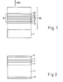
- a superlattice structure in accordance with the present invention is shown and generally designated by the reference numeral 200.
- the superlattice structure 200 is provided on a GaAs substrate 1 and made up of at least several tens to several hundreds of unit structures 50 which are sequentially laminated in the ⁇ 100> direction of the GaAs substrate 1.
- Each of the unit structures 50 defines one period and comprises an InP single atomic layer 21, an AlP single atomic layer 31, an InP single atomic layer 22, a GaP single atomic layer 40, an InP single atomic layer 23, and an AlP single atomic layer 32.
- the superlattice structure corresponds to Al 0.33 Ga 0.17 In 0.5 P.
- each of the layers in the unit structure may be selected within the range of one to ten atomic layers, instead of a single atomic layer shown and described.
- the energy gap of a superlattice structure is substantially determined by an average composition, it is possible to attain any desired bandgap by controlling the thickness of each layer. Whatever order may be selected for the layers in the unit structure, the indirect-to-direct energy gap transformation effect is utilized.
- the semiconductor laser comprises an n-GaAs substrate 2, and a cladding layer 6, an active layer 5 having a superlattice structure and a cladding layer 7 which are sequentially provided on the substrate 2 by molecular beam epitaxy.
- An n-type electrode 10 is provided on the substrate 10 and a p-type electrode 11 on the cladding layer 7.
- the active layer 5 having the superlattice shown in FIG. 1 has a total thickness of about 0.1 micron and an average composition which corresponds to Al 0.33 Ga 0.17 In 0.5 P.
- the cladding layer 6 and 7 respectively comprise n-Al 0.5 In 0.5 P and p-Al 0.5 In 0.5 P and each have a greater effective energy gap than the superlattice structure.
- the cladding layers 6 and 7 constitute a double-heterostructure together with the active layer 5. In this structure, injected electrons and light can be effectively confined in the active layer 5.
- a light emitting diode, semiconductor laser or like light emitting element whose emission wavelength is as short as 560 nanometers or less can be implemented only with a III-V compound semiconductor by using, as an active layer of the light emitting element, a semiconductor superlattice structure which is made up of an AlP layer, a GaP layer and an InP layer each being one to ten atomic layers thick.
Landscapes
- Physics & Mathematics (AREA)
- Engineering & Computer Science (AREA)
- Nanotechnology (AREA)
- Optics & Photonics (AREA)
- Chemical & Material Sciences (AREA)
- Crystallography & Structural Chemistry (AREA)
- Biophysics (AREA)
- Life Sciences & Earth Sciences (AREA)
- Condensed Matter Physics & Semiconductors (AREA)
- General Physics & Mathematics (AREA)
- Electromagnetism (AREA)
- Semiconductor Lasers (AREA)
- Led Devices (AREA)
Applications Claiming Priority (2)
| Application Number | Priority Date | Filing Date | Title |
|---|---|---|---|
| JP200207/84 | 1984-09-25 | ||
| JP59200207A JPH0728080B2 (ja) | 1984-09-25 | 1984-09-25 | 半導体超格子構造体 |
Publications (3)
| Publication Number | Publication Date |
|---|---|
| EP0176087A2 true EP0176087A2 (de) | 1986-04-02 |
| EP0176087A3 EP0176087A3 (en) | 1988-06-01 |
| EP0176087B1 EP0176087B1 (de) | 1993-07-14 |
Family
ID=16420584
Family Applications (1)
| Application Number | Title | Priority Date | Filing Date |
|---|---|---|---|
| EP85112133A Expired - Lifetime EP0176087B1 (de) | 1984-09-25 | 1985-09-24 | Halbleiterübergitterstruktur |
Country Status (4)
| Country | Link |
|---|---|
| US (1) | US4675708A (de) |
| EP (1) | EP0176087B1 (de) |
| JP (1) | JPH0728080B2 (de) |
| DE (1) | DE3587451T2 (de) |
Cited By (4)
| Publication number | Priority date | Publication date | Assignee | Title |
|---|---|---|---|---|
| GB2193598A (en) * | 1986-08-08 | 1988-02-10 | Sharp Kk | A semiconductor laser device |
| EP0200460A3 (de) * | 1985-04-22 | 1988-12-14 | Sharp Kabushiki Kaisha | Halbleiterlaservorrichtung |
| EP0284031A3 (de) * | 1987-03-25 | 1989-03-29 | Hitachi, Ltd. | Optoelektronische Vorrichtung |
| EP0287067A3 (en) * | 1987-04-14 | 1989-11-29 | Canon Kabushiki Kaisha | Electron emission device |
Families Citing this family (12)
| Publication number | Priority date | Publication date | Assignee | Title |
|---|---|---|---|---|
| JPS61136803A (ja) * | 1984-12-07 | 1986-06-24 | 極東開発工業株式会社 | 塵芥収集車の押込機構 |
| JPH0669109B2 (ja) * | 1984-12-07 | 1994-08-31 | シャ−プ株式会社 | 光半導体装置 |
| JPS61210679A (ja) * | 1985-03-15 | 1986-09-18 | Sony Corp | 半導体装置 |
| KR900002687B1 (ko) * | 1985-12-16 | 1990-04-23 | 후지쓰가부시끼가이샤 | Mbe법에 의한 기판에 격자 정합시키는 4원 또는 5원 흔정 반도체의 성장방법 |
| US4769341A (en) * | 1986-12-29 | 1988-09-06 | American Telephone And Telegraph Company, At&T Bell Laboratories | Method of fabricating non-silicon materials on silicon substrate using an alloy of Sb and Group IV semiconductors |
| EP0323249B1 (de) * | 1987-12-29 | 1993-11-03 | Nec Corporation | Halbleiterkristallstruktur und deren Herstellungsverfahren |
| US4905056A (en) * | 1988-09-30 | 1990-02-27 | Berndt Dale F | Superlattice precision voltage reference |
| DE69707390T2 (de) * | 1996-04-24 | 2002-06-27 | Uniphase Opto Holdings Inc., San Jose | Strahlungsemittierende halbleiterdiode und deren herstellungsverfahren |
| US6570179B1 (en) | 1998-01-14 | 2003-05-27 | Mp Technologies, Llc | III-V semiconductors separate confinement superlattice optoelectronic devices |
| GB2344932A (en) | 1998-12-15 | 2000-06-21 | Sharp Kk | Semiconductor Laser with gamma and X electron barriers |
| US6586762B2 (en) | 2000-07-07 | 2003-07-01 | Nichia Corporation | Nitride semiconductor device with improved lifetime and high output power |
| AT528275A1 (de) * | 2024-04-30 | 2025-11-15 | Univ Linz | Vorrichtung zur Laserstrahlenemission |
Family Cites Families (3)
| Publication number | Priority date | Publication date | Assignee | Title |
|---|---|---|---|---|
| US4205329A (en) * | 1976-03-29 | 1980-05-27 | Bell Telephone Laboratories, Incorporated | Periodic monolayer semiconductor structures grown by molecular beam epitaxy |
| US4261771A (en) * | 1979-10-31 | 1981-04-14 | Bell Telephone Laboratories, Incorporated | Method of fabricating periodic monolayer semiconductor structures by molecular beam epitaxy |
| JPH0669109B2 (ja) * | 1984-12-07 | 1994-08-31 | シャ−プ株式会社 | 光半導体装置 |
-
1984
- 1984-09-25 JP JP59200207A patent/JPH0728080B2/ja not_active Expired - Lifetime
-
1985
- 1985-09-24 EP EP85112133A patent/EP0176087B1/de not_active Expired - Lifetime
- 1985-09-24 US US06/779,756 patent/US4675708A/en not_active Expired - Lifetime
- 1985-09-24 DE DE85112133T patent/DE3587451T2/de not_active Expired - Fee Related
Cited By (6)
| Publication number | Priority date | Publication date | Assignee | Title |
|---|---|---|---|---|
| EP0200460A3 (de) * | 1985-04-22 | 1988-12-14 | Sharp Kabushiki Kaisha | Halbleiterlaservorrichtung |
| GB2193598A (en) * | 1986-08-08 | 1988-02-10 | Sharp Kk | A semiconductor laser device |
| US4860297A (en) * | 1986-08-08 | 1989-08-22 | Sharp Kabushiki Kaisha | Quantum well semiconductor laser device |
| GB2193598B (en) * | 1986-08-08 | 1990-12-12 | Sharp Kk | A semiconductor laser device |
| EP0284031A3 (de) * | 1987-03-25 | 1989-03-29 | Hitachi, Ltd. | Optoelektronische Vorrichtung |
| EP0287067A3 (en) * | 1987-04-14 | 1989-11-29 | Canon Kabushiki Kaisha | Electron emission device |
Also Published As
| Publication number | Publication date |
|---|---|
| US4675708A (en) | 1987-06-23 |
| DE3587451T2 (de) | 1994-01-20 |
| JPS6178189A (ja) | 1986-04-21 |
| EP0176087A3 (en) | 1988-06-01 |
| EP0176087B1 (de) | 1993-07-14 |
| JPH0728080B2 (ja) | 1995-03-29 |
| DE3587451D1 (de) | 1993-08-19 |
Similar Documents
| Publication | Publication Date | Title |
|---|---|---|
| US4675708A (en) | Semiconductor superlattice structure | |
| US5610413A (en) | Group II-VI compound semiconductor light emitting devices and an ohmic contact therefor | |
| US4794611A (en) | Semiconductor laser having superlattice structure | |
| US4974231A (en) | Visible light semiconductor laser | |
| JPH09510831A (ja) | 量子層の構造 | |
| EP0610893B1 (de) | Diodenlaser | |
| US5473173A (en) | Quantum well structure having differentially strained quantum well layers | |
| EP0188080B1 (de) | Lichtemittierende Halbleiteranordnung mit einem Übergitter | |
| JP2784093B2 (ja) | 半導体装置 | |
| US5714014A (en) | Semiconductor heterojunction material | |
| JPH07231142A (ja) | 半導体発光素子 | |
| JPH09199783A (ja) | 半導体発光素子 | |
| JPH0554279B2 (de) | ||
| EP0334759B1 (de) | Halbleiterlaser-Vorrichtung | |
| JPH07112089B2 (ja) | 半導体発光装置 | |
| JPH077218A (ja) | 半導体レーザ | |
| JPH05347432A (ja) | 半導体発光素子 | |
| JPH03257887A (ja) | 半導体レーザ装置 | |
| JPH0794822A (ja) | 半導体発光素子 | |
| US5362974A (en) | Group II-VI material semiconductor optical device with strained multiquantum barriers | |
| JP2833604B2 (ja) | 半導体積層構造 | |
| US5859865A (en) | Semiconductor laser | |
| JPS6052067A (ja) | 超格子の構造 | |
| EP0396704A1 (de) | Lichtemittierendes halbleiterbauelement | |
| JP2708799B2 (ja) | 量子井戸構造型半導体レーザー装置 |
Legal Events
| Date | Code | Title | Description |
|---|---|---|---|
| PUAI | Public reference made under article 153(3) epc to a published international application that has entered the european phase |
Free format text: ORIGINAL CODE: 0009012 |
|
| 17P | Request for examination filed |
Effective date: 19850924 |
|
| AK | Designated contracting states |
Kind code of ref document: A2 Designated state(s): DE FR GB NL |
|
| PUAL | Search report despatched |
Free format text: ORIGINAL CODE: 0009013 |
|
| AK | Designated contracting states |
Kind code of ref document: A3 Designated state(s): DE FR GB NL |
|
| 17Q | First examination report despatched |
Effective date: 19900718 |
|
| GRAA | (expected) grant |
Free format text: ORIGINAL CODE: 0009210 |
|
| AK | Designated contracting states |
Kind code of ref document: B1 Designated state(s): DE FR GB NL |
|
| PG25 | Lapsed in a contracting state [announced via postgrant information from national office to epo] |
Ref country code: NL Effective date: 19930714 Ref country code: FR Effective date: 19930714 |
|
| REF | Corresponds to: |
Ref document number: 3587451 Country of ref document: DE Date of ref document: 19930819 |
|
| EN | Fr: translation not filed | ||
| NLV1 | Nl: lapsed or annulled due to failure to fulfill the requirements of art. 29p and 29m of the patents act | ||
| PLBE | No opposition filed within time limit |
Free format text: ORIGINAL CODE: 0009261 |
|
| STAA | Information on the status of an ep patent application or granted ep patent |
Free format text: STATUS: NO OPPOSITION FILED WITHIN TIME LIMIT |
|
| 26N | No opposition filed | ||
| REG | Reference to a national code |
Ref country code: GB Ref legal event code: IF02 |
|
| PGFP | Annual fee paid to national office [announced via postgrant information from national office to epo] |
Ref country code: GB Payment date: 20020918 Year of fee payment: 18 |
|
| PGFP | Annual fee paid to national office [announced via postgrant information from national office to epo] |
Ref country code: DE Payment date: 20021002 Year of fee payment: 18 |
|
| PG25 | Lapsed in a contracting state [announced via postgrant information from national office to epo] |
Ref country code: GB Free format text: LAPSE BECAUSE OF NON-PAYMENT OF DUE FEES Effective date: 20030924 |
|
| PG25 | Lapsed in a contracting state [announced via postgrant information from national office to epo] |
Ref country code: DE Free format text: LAPSE BECAUSE OF NON-PAYMENT OF DUE FEES Effective date: 20040401 |
|
| GBPC | Gb: european patent ceased through non-payment of renewal fee |
Effective date: 20030924 |