EP0176111A1 - Système de mémoire rapide non-volatile, électriquement effaçable - Google Patents
Système de mémoire rapide non-volatile, électriquement effaçable Download PDFInfo
- Publication number
- EP0176111A1 EP0176111A1 EP85112639A EP85112639A EP0176111A1 EP 0176111 A1 EP0176111 A1 EP 0176111A1 EP 85112639 A EP85112639 A EP 85112639A EP 85112639 A EP85112639 A EP 85112639A EP 0176111 A1 EP0176111 A1 EP 0176111A1
- Authority
- EP
- European Patent Office
- Prior art keywords
- lines
- voltage
- write
- sense
- memory cells
- Prior art date
- Legal status (The legal status is an assumption and is not a legal conclusion. Google has not performed a legal analysis and makes no representation as to the accuracy of the status listed.)
- Withdrawn
Links
Images


Classifications
-
- G—PHYSICS
- G11—INFORMATION STORAGE
- G11C—STATIC STORES
- G11C16/00—Erasable programmable read-only memories
- G11C16/02—Erasable programmable read-only memories electrically programmable
- G11C16/04—Erasable programmable read-only memories electrically programmable using variable threshold transistors, e.g. FAMOS
- G11C16/0408—Erasable programmable read-only memories electrically programmable using variable threshold transistors, e.g. FAMOS comprising cells containing floating gate transistors
- G11C16/0433—Erasable programmable read-only memories electrically programmable using variable threshold transistors, e.g. FAMOS comprising cells containing floating gate transistors comprising cells containing a single floating gate transistor and one or more separate select transistors
-
- H—ELECTRICITY
- H10—SEMICONDUCTOR DEVICES; ELECTRIC SOLID-STATE DEVICES NOT OTHERWISE PROVIDED FOR
- H10B—ELECTRONIC MEMORY DEVICES
- H10B41/00—Electrically erasable-and-programmable ROM [EEPROM] devices comprising floating gates
-
- H—ELECTRICITY
- H10—SEMICONDUCTOR DEVICES; ELECTRIC SOLID-STATE DEVICES NOT OTHERWISE PROVIDED FOR
- H10B—ELECTRONIC MEMORY DEVICES
- H10B69/00—Erasable-and-programmable ROM [EPROM] devices not provided for in groups H10B41/00 - H10B63/00, e.g. ultraviolet erasable-and-programmable ROM [UVEPROM] devices
Definitions
- the present invention relates to electrically erasable memory systems and in particular to a method for encoding binary data into a nonvolatile, electrically erasable memory system.
- Prior art nonvolatile memory systems have been restricted to field effect transistor, typically MOS, technology with a resultant limitation in operating speed. While it is well_known that higher operating speeds are provided by bipolar technology, prior bipolar art has lacked a nonvolatile storage mechanism.
- the present invention provides a method for high speed erasing, writing and reading binary data in an electrically erasable nonvolatile memory array.
- a method for encoding binary data into an electrically erasable memory comprising a matrix of memory cells.
- Each cell of the memory array comprises a pMOS floating gate transistor for data storage and a merged npn bipolar transistor for selective access to stored data.
- the pMOS floating gate transistor acts similarly to a current source, injecting (depending on its threshold) either finite or zero base current into the npn bipolar transistor, causing the bipolar transistor to exhibit either high or low impedance.
- the memory array comprises a matrix of such memory cells formed as a plurality of rows and a plurality of columns.
- a plurality of X write lines are provided, the control gate of each pMOS storage transistor in a row of memory cells being connected to an X write line corresponding to that row.
- a plurality of X sense lines are also provided, the emitter of each bipolar transistor in a row of cells being connected to an X sense line corresponding to that row.
- a plurality of source lines are also provided, the source of each pMOS storage transistor in a row of cells being connected to a source line corresponding to that row.
- a plurality of Y sense lines are also provided, the collector of each bipolar transistor in a column of cells being connected to a Y sense line corresponding to that column.
- continuous strips of N+ buried layer form the Y sense lines and are OR-tied to the collectors of the bipolar transistors in the corresponding column.
- Binary data is encoded into the memory array by applying an erase voltage to each of the Y sense lines in the array, and, simultaneously, maintaining each of the X sense lines at the erase voltage.
- each of the X write lines is maintained at ground and the erase voltage is applied to each of the source lines. This condition causes each of the storage transistors to assume a relatively negative threshold state.
- a write voltage is applied to selected X write lines while unselected X write lines are maintained at ground.
- selected Y sense lines are maintained at ground and an inhibit voltage which is less than the write voltage is applied to unselected Y sense lines.
- each of the X sense lines in the array is maintained at an intermediate voltage which is less than or equal to the base/emitter breakdown voltage of the bipolar transistors.
- a selected X sense line is maintained at ground while unselected X sense lines and each Y sense line are maintained at about +3 volts.
- memory cells connected to the selected X sense lines and having pMOS storage transistors in the relatively negative threshold state are less conducting than memory cells connected to the selected X sense line and having storage transistors in the relatively high threshold state.
- the memory cells connected to the selected X sense line are then monitored to determine their relative conductance.
- a preferred embodiment of a high speed nonvolatile memory cell of the invention comprises a floating gate pMOS transistor for data storage and a merged npn bipolar transistor for selective access to stored data.
- a first N+ polysilicon region forms the floating gate 22a of the pMOS storage transistor while a first P+ polysilicon region forms its control gate 26a.
- a second region of N+ polysilicon forms the emitter 22b of the npn bipolar transistor.
- a second region of P+ polysilicon forms the contact 26b to P+ epitaxial regions which form part of the base of the npn bipolar transistor.
- the N+ buried layer 13 serves as the collector of the bipolar transistor.
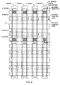
- the memory cell shown in Fig. 1 is utilized in an electrically erasable, high speed, nonvolatile memory array such as that shown in Figs. 2-4.
- the memory array comprises a matrix of memory cells of the type described above which are formed as a plurality of rows and a plurality of columns of such cells.
- Fig. 2 shows a section of the memory array topography, representing 16 bits in a 4 X 4 array.
- the memory array includes a plurality of X write lines, the control gate of each p M OS storage transistor in a row of memory cells being connected to an X write line corresponding to that row.
- the X write line comprises P+ polysilicon and forms the control gate of the pMOS transistors in that row.
- the array further includes a plurality of X sense lines, the emitter of each bipolar transistor in a row of cells being connected to an X sense line corresponding to that row.
- the" X sense line comprises N+ polysilicon and links all emitters of the npn bipolar transistors in the row.
- the array further comprises a plurality of source lines, the source of each pMOS storage transistor in a row of cells being connected to a source line corresponding to that row.
- the array further includes a plurality of Y sense lines, the collector of each npn bipolar transistor in a column of memory cells being connected to a Y sense line corresponding to that column.
- orthogonal strips of N+ buried layer form the Y sense lines and are OR-tied to the collectors of the npn bipolar transistors.
- an erase voltage is applied to each of the Y sense lines.
- each of the X sense lines is maintained at the erase voltage
- each of the X write lines is maintained at ground and the erase voltage is applied to each of the source lines.
- each of the storage transistors in the array assumes a relatively negative threshold state.
- a memory cell having a relatively negative threshold state is relatively less conducting when a read voltage is applied.
- a write voltage preferably about +20 volts, is applied to selected X write lines while maintaining unselected X write lines at ground.
- selected Y sense lines are maintained at ground and an inhibit voltage, preferably about +5 volts, is applied to unselected Y sense lines.
- the inhibit voltage inhibits threshold shift by reducing the field across the thin oxide beneath the floating gate of the pMOS storage transistor.
- the inhibit voltage is insufficient to cause any significant threshold disturbance in unselected devices over many cycles of data change.
- each of the X sense lines is maintained at an intermediate voltage, which intermediate voltage is between the write voltage and the inhibit voltage and preferably is about +10 volts.
- the intermediate voltage is equal to or less than the base/emitter breakdown voltage of the npn bipolar transistors in the array.
- the pMOS storage transistors of memory cells located at the intersections of selected X write lines and selected Y sense lines assume a relatively positive threshold state while the remaining memory cells remain at the relatively negative threshold state.
- a memory cell in a relatively positive threshold state is relatively more conducting when a read voltage is applied.
- a selected X sense line is maintained at ground. Simultaneously, unselected X sense lines and each of the Y sense lines are maintained at about +3 to +5 volts. At these conditions, memory cells connected to the selected X sense line and having pMOS storage transistors in the relatively negative threshold state are less conducting than memory cells connected to the selected X sense line and having pMOS storage transistors in the relatively positive threshold state. Memory cells connected to the selected X sense lines are monitored to determine their relative conductance.
- Table I provides a summary of operating conditions for the array.
Landscapes
- Engineering & Computer Science (AREA)
- Microelectronics & Electronic Packaging (AREA)
- Semiconductor Memories (AREA)
- Non-Volatile Memory (AREA)
- Read Only Memory (AREA)
Applications Claiming Priority (2)
| Application Number | Priority Date | Filing Date | Title |
|---|---|---|---|
| US219784 | 1980-12-24 | ||
| US06/219,784 US4398338A (en) | 1980-12-24 | 1980-12-24 | Fabrication of high speed, nonvolatile, electrically erasable memory cell and system utilizing selective masking, deposition and etching techniques |
Related Parent Applications (1)
| Application Number | Title | Priority Date | Filing Date |
|---|---|---|---|
| EP81402036.8 Division | 1981-12-21 |
Publications (1)
| Publication Number | Publication Date |
|---|---|
| EP0176111A1 true EP0176111A1 (fr) | 1986-04-02 |
Family
ID=22820767
Family Applications (2)
| Application Number | Title | Priority Date | Filing Date |
|---|---|---|---|
| EP85112639A Withdrawn EP0176111A1 (fr) | 1980-12-24 | 1981-12-21 | Système de mémoire rapide non-volatile, électriquement effaçable |
| EP81402036A Expired EP0055182B1 (fr) | 1980-12-24 | 1981-12-21 | Cellule et système de mémoire non volatile rapide et électriquement altérable |
Family Applications After (1)
| Application Number | Title | Priority Date | Filing Date |
|---|---|---|---|
| EP81402036A Expired EP0055182B1 (fr) | 1980-12-24 | 1981-12-21 | Cellule et système de mémoire non volatile rapide et électriquement altérable |
Country Status (4)
| Country | Link |
|---|---|
| US (1) | US4398338A (fr) |
| EP (2) | EP0176111A1 (fr) |
| JP (1) | JPS57172774A (fr) |
| DE (1) | DE3175509D1 (fr) |
Cited By (1)
| Publication number | Priority date | Publication date | Assignee | Title |
|---|---|---|---|---|
| EP0354457A3 (en) * | 1988-08-08 | 1990-10-17 | National Semiconductor Corporation | A bipolar field-effect electrically erasable programmable read only memory cell and method of manufacture |
Families Citing this family (20)
| Publication number | Priority date | Publication date | Assignee | Title |
|---|---|---|---|---|
| US4433470A (en) | 1981-05-19 | 1984-02-28 | Tokyo Shibaura Denki Kabushiki Kaisha | Method for manufacturing semiconductor device utilizing selective etching and diffusion |
| US4488350A (en) * | 1981-10-27 | 1984-12-18 | Fairchild Camera & Instrument Corp. | Method of making an integrated circuit bipolar memory cell |
| US4617071A (en) * | 1981-10-27 | 1986-10-14 | Fairchild Semiconductor Corporation | Method of fabricating electrically connected regions of opposite conductivity type in a semiconductor structure |
| US4622575A (en) * | 1981-10-27 | 1986-11-11 | Fairchild Semiconductor Corporation | Integrated circuit bipolar memory cell |
| US4507848A (en) * | 1982-11-22 | 1985-04-02 | Fairchild Camera & Instrument Corporation | Control of substrate injection in lateral bipolar transistors |
| US4527325A (en) * | 1983-12-23 | 1985-07-09 | International Business Machines Corporation | Process for fabricating semiconductor devices utilizing a protective film during high temperature annealing |
| US5243210A (en) * | 1987-02-21 | 1993-09-07 | Kabushiki Kaisha Toshiba | Semiconductor memory device and manufacturing method thereof |
| US5089433A (en) * | 1988-08-08 | 1992-02-18 | National Semiconductor Corporation | Bipolar field-effect electrically erasable programmable read only memory cell and method of manufacture |
| US5089429A (en) * | 1989-06-22 | 1992-02-18 | David Sarnoff Research Center, Inc. | Self-aligned emitter bicmos process |
| IT1237666B (it) * | 1989-10-31 | 1993-06-15 | Sgs Thomson Microelectronics | Processo per la fabbricazione di un componente limitatore della tensione di programmazione e stabilizzatore di tensione incorporato inun dispositivo elettrico con celle di memoria eeprom |
| JPH07123145B2 (ja) * | 1990-06-27 | 1995-12-25 | 株式会社東芝 | 半導体集積回路 |
| US5225700A (en) * | 1991-06-28 | 1993-07-06 | Texas Instruments Incorporated | Circuit and method for forming a non-volatile memory cell |
| US6534364B1 (en) * | 1994-12-05 | 2003-03-18 | Texas Instruments Incorporated | Tunnel diode layout for an EEPROM cell for protecting the tunnel diode region |
| US5576233A (en) * | 1995-06-21 | 1996-11-19 | Texas Instruments Incorporated | Method for making an EEPROM with thermal oxide isolated floating gate |
| US5747383A (en) * | 1995-09-05 | 1998-05-05 | Taiwan Semiconductor Manufacturing Company Ltd | Method for forming conductive lines and stacked vias |
| US5717635A (en) * | 1996-08-27 | 1998-02-10 | International Business Machines Corporation | High density EEPROM for solid state file |
| US6060360A (en) * | 1997-04-14 | 2000-05-09 | Taiwan Semiconductor Manufacturing Company | Method of manufacture of P-channel EEprom and flash EEprom devices |
| US7745301B2 (en) | 2005-08-22 | 2010-06-29 | Terapede, Llc | Methods and apparatus for high-density chip connectivity |
| US8957511B2 (en) | 2005-08-22 | 2015-02-17 | Madhukar B. Vora | Apparatus and methods for high-density chip connectivity |
| US8320191B2 (en) | 2007-08-30 | 2012-11-27 | Infineon Technologies Ag | Memory cell arrangement, method for controlling a memory cell, memory array and electronic device |
Citations (2)
| Publication number | Priority date | Publication date | Assignee | Title |
|---|---|---|---|---|
| US3893085A (en) * | 1973-11-28 | 1975-07-01 | Ibm | Read mostly memory cell having bipolar and FAMOS transistor |
| FR2296939A1 (fr) * | 1975-01-06 | 1976-07-30 | Ncr Co | Dispositif semi-conducteur a quatre zones |
Family Cites Families (9)
| Publication number | Priority date | Publication date | Assignee | Title |
|---|---|---|---|---|
| US3609479A (en) * | 1968-02-29 | 1971-09-28 | Westinghouse Electric Corp | Semiconductor integrated circuit having mis and bipolar transistor elements |
| US3648125A (en) * | 1971-02-02 | 1972-03-07 | Fairchild Camera Instr Co | Method of fabricating integrated circuits with oxidized isolation and the resulting structure |
| US3996657A (en) * | 1974-12-30 | 1976-12-14 | Intel Corporation | Double polycrystalline silicon gate memory device |
| US4258378A (en) * | 1978-05-26 | 1981-03-24 | Texas Instruments Incorporated | Electrically alterable floating gate memory with self-aligned low-threshold series enhancement transistor |
| US4234362A (en) * | 1978-11-03 | 1980-11-18 | International Business Machines Corporation | Method for forming an insulator between layers of conductive material |
| US4168999A (en) * | 1978-12-26 | 1979-09-25 | Fairchild Camera And Instrument Corporation | Method for forming oxide isolated integrated injection logic semiconductor structures having minimal encroachment utilizing special masking techniques |
| US4247861A (en) * | 1979-03-09 | 1981-01-27 | Rca Corporation | High performance electrically alterable read-only memory (EAROM) |
| US4237472A (en) * | 1979-03-12 | 1980-12-02 | Rca Corporation | High performance electrically alterable read only memory (EAROM) |
| US4322883A (en) * | 1980-07-08 | 1982-04-06 | International Business Machines Corporation | Self-aligned metal process for integrated injection logic integrated circuits |
-
1980
- 1980-12-24 US US06/219,784 patent/US4398338A/en not_active Expired - Lifetime
-
1981
- 1981-12-21 EP EP85112639A patent/EP0176111A1/fr not_active Withdrawn
- 1981-12-21 EP EP81402036A patent/EP0055182B1/fr not_active Expired
- 1981-12-21 DE DE8181402036T patent/DE3175509D1/de not_active Expired
- 1981-12-24 JP JP20827181A patent/JPS57172774A/ja active Pending
Patent Citations (2)
| Publication number | Priority date | Publication date | Assignee | Title |
|---|---|---|---|---|
| US3893085A (en) * | 1973-11-28 | 1975-07-01 | Ibm | Read mostly memory cell having bipolar and FAMOS transistor |
| FR2296939A1 (fr) * | 1975-01-06 | 1976-07-30 | Ncr Co | Dispositif semi-conducteur a quatre zones |
Non-Patent Citations (1)
| Title |
|---|
| IBM TECHNICAL DISCLOSURE BULLETIN, vol. 22, no. 12, May 1980, pages 5296-5297, New York, US; D.M. KENNEY: "Bipolar erase technique in EPROM VMOS devices" * |
Cited By (1)
| Publication number | Priority date | Publication date | Assignee | Title |
|---|---|---|---|---|
| EP0354457A3 (en) * | 1988-08-08 | 1990-10-17 | National Semiconductor Corporation | A bipolar field-effect electrically erasable programmable read only memory cell and method of manufacture |
Also Published As
| Publication number | Publication date |
|---|---|
| JPS57172774A (en) | 1982-10-23 |
| EP0055182A3 (en) | 1983-06-22 |
| US4398338A (en) | 1983-08-16 |
| EP0055182A2 (fr) | 1982-06-30 |
| DE3175509D1 (en) | 1986-11-27 |
| EP0055182B1 (fr) | 1986-10-22 |
Similar Documents
| Publication | Publication Date | Title |
|---|---|---|
| EP0176111A1 (fr) | Système de mémoire rapide non-volatile, électriquement effaçable | |
| US5465231A (en) | EEPROM and logic LSI chip including such EEPROM | |
| US5402373A (en) | Electrically erasable programmable read-only memory with electric field decreasing controller | |
| US5590068A (en) | Ultra-high density alternate metal virtual ground ROM | |
| KR950010725B1 (ko) | 불휘발성 반도체기억장치 | |
| US5841700A (en) | Source-coupling, split gate, virtual ground flash EEPROM array | |
| US7110320B2 (en) | Nonvolatile semiconductor memory | |
| US6091633A (en) | Memory array architecture utilizing global bit lines shared by multiple cells | |
| US6380636B1 (en) | Nonvolatile semiconductor memory device having an array structure suitable to high-density integrationization | |
| US3986180A (en) | Depletion mode field effect transistor memory system | |
| US6226214B1 (en) | Read only memory | |
| JPH0760864B2 (ja) | 半導体集積回路装置 | |
| KR20020042441A (ko) | 반도체장치, ic카드 및 반도체장치의 제조방법 | |
| KR960016106B1 (ko) | 비 휘발성 반도체 메모리 장치 | |
| JPH08500937A (ja) | ソース側注入を用いた分離ゲートを備えたeeprom | |
| US4126899A (en) | Junction field effect transistor random access memory | |
| US6310800B1 (en) | Non-volatile semiconductor memory device and method for driving the same | |
| GB1593002A (en) | Semiconductor devices | |
| US6504191B2 (en) | Independently programmable memory segments within a PMOS electrically erasable programmable read only memory array achieved by N-well separation and method therefor | |
| US4435790A (en) | High speed, nonvolatile, electrically erasable memory cell and system | |
| US5179427A (en) | Non-volatile semiconductor memory device with voltage stabilizing electrode | |
| KR960010736B1 (ko) | 마스크 rom 및 그 제조방법 | |
| US5400279A (en) | Nonvolatile semiconductor memory device with NAND cell structure | |
| KR960000723B1 (ko) | Eeprom | |
| US5471423A (en) | Non-volatile semiconductor memory device |
Legal Events
| Date | Code | Title | Description |
|---|---|---|---|
| PUAI | Public reference made under article 153(3) epc to a published international application that has entered the european phase |
Free format text: ORIGINAL CODE: 0009012 |
|
| AC | Divisional application: reference to earlier application |
Ref document number: 55182 Country of ref document: EP |
|
| AK | Designated contracting states |
Kind code of ref document: A1 Designated state(s): DE FR GB IT NL |
|
| 17P | Request for examination filed |
Effective date: 19860925 |
|
| STAA | Information on the status of an ep patent application or granted ep patent |
Free format text: STATUS: THE APPLICATION IS DEEMED TO BE WITHDRAWN |
|
| 18D | Application deemed to be withdrawn |
Effective date: 19870603 |
|
| RIN1 | Information on inventor provided before grant (corrected) |
Inventor name: VORA, MADHUKAR B. Inventor name: TICKLE, ANDREW |