EP0176114A2 - Circuit d'échantillonage et de maintien à offset de zéro automatique - Google Patents
Circuit d'échantillonage et de maintien à offset de zéro automatique Download PDFInfo
- Publication number
- EP0176114A2 EP0176114A2 EP85201171A EP85201171A EP0176114A2 EP 0176114 A2 EP0176114 A2 EP 0176114A2 EP 85201171 A EP85201171 A EP 85201171A EP 85201171 A EP85201171 A EP 85201171A EP 0176114 A2 EP0176114 A2 EP 0176114A2
- Authority
- EP
- European Patent Office
- Prior art keywords
- inverting
- circuit
- output
- during
- hold
- Prior art date
- Legal status (The legal status is an assumption and is not a legal conclusion. Google has not performed a legal analysis and makes no representation as to the accuracy of the status listed.)
- Granted
Links
Images

Classifications
-
- G—PHYSICS
- G11—INFORMATION STORAGE
- G11C—STATIC STORES
- G11C27/00—Electric analogue stores, e.g. for storing instantaneous values
- G11C27/02—Sample-and-hold arrangements
-
- G—PHYSICS
- G11—INFORMATION STORAGE
- G11C—STATIC STORES
- G11C27/00—Electric analogue stores, e.g. for storing instantaneous values
- G11C27/02—Sample-and-hold arrangements
- G11C27/024—Sample-and-hold arrangements using a capacitive memory element
- G11C27/026—Sample-and-hold arrangements using a capacitive memory element associated with an amplifier
Definitions
- This invention relates to the electronic sample and hold circuits having offset voltage cancellation. This invention relates in particular to:
- Circuits that switch between a sample mode and a hold mode are used widely.
- a sample mode such a sample and hold (S/H) circuit tracks an analog input voltage.
- the S/H circuit stores the value of the input voltage that existed just before the circuit switched from sample to hold.
- An important objective is designing an S/H circuit is to minimize the offset voltage error in the circuit output signal provided during hold.
- One way of doing this is to arrange the circuit in such a manner that-the total voltage offset occurring during sample is of largely the same magnitude but opposite sign to that occurring during hold so that the offsets cancel. This technique is referred to as auto-zeroing.
- U.S. Patents 3,696,305, 4,119,960 and 4,302,689 disclose auto-zero S/H circuits. Each of these circuits contains an operational amplifier (ehereafter "op amp") whose output voltage slews through at least the value of the analog input voltage when the circuit switches from sample to hold. Because the circuit has to settle before a steady-state value is reached for the output voltage, the acquisition time in the hold mode is high.
- op amp operational amplifier
- a sample and hold circuit of the kind mentioned in the opening paragraph is known from F. Gasparik, "An Autozeroing Sample and Hold IC", 1980 IEEE Int'l Soldi-State Circs. Conf., Dig. Tech. Paps., February 1980, pags. 132-133. This article describes an S/H circuit that achieves excellent offset voltage cancellation with less slewing than in the foregoing patents.
- a disadvantage of the Gasparik circuit is that it has to settle twice during sample and hold operation. This substantially increases the total acquisition time
- a sample and hold circuit of the type particularly described in the first paragraph is characterized in that the storage capacitor is coupled to the inverting input of the first means and in that the circuit further comprises a third switch for selectively coupling the non-inverting and inverting outputs of the first means respectively to the non-inverting and inverting inputs of the second means during the sample mode or respectively to the inverting and non-inverting inputs of the second means during the hold mode.
- non-inverting input and “inverting input” mean the input terminals of a differential amplifying device whose amplified open-loop output signal is substantially in phase with the differential input signal formed by the signal at the non-inverting input relative tothe signal at the inverting input. If the output signal is provided differebtially from the device, “non-inverting output” and “inverting output” mean the device output terminals between which the differential output signal exists.
- the open-loop signal at the non-inverting output is substantially in phase with the differential input signal, whereas the open-loop signal at the inverting output is substantially reversed in phase - i.e. opposite in polarity - to the differential input signal. If only a single non-inverting output terminal of the device is utilized for providing the output signal, this terminal is referred to simply as the "output” or "regular output”.
- the first switch couples the non-inverting input of the first amplifier to a circuit input terminal for receiving an input signal while the second switch couples the output of the second amplifier to the inverting input of the first amplifier.
- the third switch couples the non-inverting and inverting outputs of the first amplifier respectively to the non-inverting and inverting inputs of the second amplifier.
- the first switch couples the non-inverting input of the first amplifier to the output of the second amplifier while the second switch couples the output of the second amplifier to a high-impedance position.
- the third switch reverses the connections of the outputs of the first amplifier so that they are respectively coupled to the inverting and non-inverting inputs of the second amplifier.
- the circuit output signal is taken at the output of the second amplifier.
- the circuit output signal during hold follows the same path through the first amplifier that the circuit input signal did during sample.
- the input and output signals thus experience the same offset error in the first amplifier.
- the offset of the first amplifier is cancelled out of the output signal, while the effect of the offset of the second amplifier is reduced by a factor proportional to the gain of the first amplifier. If the amplifier gains are very high, the total error between the input and output signals is virtually zero.
- the common-mode rejection ratio is extremely high.
- the circuit thereby provides high accuracy with fast response.
- Fig. 1 illustrates an auto-zero S/H circuit that switches between a sample mode during which an input voltage V IN is tracked and a hold mode during which an output voltage V OUT is provided at a value largely equal to the VIN value existing at the end of the sample mode.
- the voltage offsets occurring in the sample mode for the circuit are substantially cancelled by those occurring in the hold mode.
- Fig. 2a shows the operational connections when the circuit is in sample.
- Fig. 2b shows the operational connections for hold.
- Amplifier A1 is a differential output device. It amplifies the differential voltage ⁇ 1 between its non-inverting (+) and inverting inputs by a factor A to provide an amplified differential voltage d V between its non-inverting (+) and inverting (-) outputs.
- Amplifier A2 amplifies the differential voltage ⁇ 2 between its non-inverting (+) abd inverting (-) inputs by a factor A 2 to provide its regular output with an amplified signal voltage taken relative to V EE .
- a storage capacitor C is connected between the A1 inverting input and the V EE supply.
- Switch S1 connects the A1 non-inverting input to a circuit input for receiving vol- ta g e V IN during sample or to the A2 output during hold.
- Switch S2 connects the A2 output to the A1 inverting input during sample or to an open-circuit (and therefore high-impedance) position, represented as NC, during hold.
- Switch S3 consisting of sub-switches S3A and S3B connects the non-inverting and inverting outputs of amplifier A1 respectively to the non-inverting and inverting inputs of amplifier A2 during sample. These connections are reversed during hold. That is, switch S3 connects the A1 non-inverting and inverting outputs respectively to the A2 inverting and non-inverting inputs.
- Voltage VOUT is the output signal of amplifier A2 during hold. As indicated in Fig.. 1, signal VOUT is preferably taken from a terminal connected permanently to the A2 output. Alternatively, signal V OUT could be taken from a terminal connected permanently to the A1 non-inverting input so that the A2 output is connected to the circuit output only during hold.
- each amplifier A1 or A2 has an internal offset voltage that causes its output voltage to be non-zero when its differential input voltage is zero.
- offset voltages V OS1 and V OS2 are schematically represented by offset voltages V OS1 and V OS2 at the respective A1 and A2 non-inverting inputs. Offsets V OS1 and V OS2 could as well be represented at the A1 and A2 inverting inputs. The results are the same with either representation.
- Block A in Fig. 2a represents this op amp. Its non-inverting input receives voltage V IN at the A1 non-inverting input, while its inverting input at the A1 inverting input is connected directly to its output at the A2 output. Gains A 1 and A 2 are quite high. As a result, capacitor C is charged to a voltage V c that closely follows voltage V IN .
- capacitor C holds voltage V c at the value existing just before the circuit switched.
- the circuit again functions as an op amp in a stable negative-feedback voltage-following configuration. This time, however, the arrangement is basically reversed as indicated by block B in Fig. 2b for the op amp. Its non-inverting input is connected to the A1 inverting input to receive voltage V C .
- the inverting input of op amp B is connected directly to its output at the A2 output where voltage V OUT is generated and held.
- each of voltages V OUT and V c is approximately V IN . Taking this into account, Eq. (7) becomes:
- the parenthetical portion of the first term on the right hand side of Eq. (8) is the normal error factor that occurs in an S/H circuit using two differential amplifiers in series.
- the normal error is quite small since gains A 1 and A 2 are each typically on the order of 10 3 .
- the present S/H circuit thus has output characteristics comparable to those of standard S/H circuits using a serial pair of differential amplifiers, except that offset V OS1 has no effect on voltage V OUT and the effect of offset V OS2 is drastically reduced.
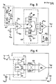
- Fig. 3 illistrates an embodiment of Fig. 1 in which switches S1 - S3 are implemented with N-channel insulated-gate field-effect transistors (FET's) Q1 - Q8 arranged as shown in an integrated circuit.
- FET's N-channel insulated-gate field-effect transistors
- Each FET has its own P well. As indicated by the arrows, the well for each FET is connected to its source. The opposite element of each FET is its drain. The gate of each FET responds either to a signal ⁇ or to a complementary signal as shown. If ⁇ is high so that is low, the circuit of Fig. 3 is in the sample mode.
- FET's Q1, Q2, Q4, Q5 and Q7 are turned on, whereas FET's Q3, Q6 and Q8 are turned off.
- Amplifiers A1 and A2 are typically op amps of conventional type, except that an inverting output signal is taken from amplifier A1. Devices other than simple op amps may, however, be used for amplifiers A1 and A2.
- Fig. 4 depicts an embldiment of Fig. 1 in which amplifier A1 consists of op amps A1 and A2 and resistors R1, R2 and R3 arranged as shown and operable in a manner known in the analog electronics art.
- the circuit is preferably fabricated in monolithic integrated circuit form according to conventional complementary metal-oxide semiconductor techniques.
Landscapes
- Amplifiers (AREA)
- Analogue/Digital Conversion (AREA)
- Mechanical Treatment Of Semiconductor (AREA)
Applications Claiming Priority (2)
| Application Number | Priority Date | Filing Date | Title |
|---|---|---|---|
| US06/644,744 US4587443A (en) | 1984-08-27 | 1984-08-27 | Auto-zero sample and hold circuit |
| US644744 | 1984-08-27 |
Publications (3)
| Publication Number | Publication Date |
|---|---|
| EP0176114A2 true EP0176114A2 (fr) | 1986-04-02 |
| EP0176114A3 EP0176114A3 (en) | 1988-01-13 |
| EP0176114B1 EP0176114B1 (fr) | 1992-01-08 |
Family
ID=24586163
Family Applications (1)
| Application Number | Title | Priority Date | Filing Date |
|---|---|---|---|
| EP85201171A Expired - Lifetime EP0176114B1 (fr) | 1984-08-27 | 1985-07-12 | Circuit d'échantillonage et de maintien à offset de zéro automatique |
Country Status (6)
| Country | Link |
|---|---|
| US (1) | US4587443A (fr) |
| EP (1) | EP0176114B1 (fr) |
| JP (1) | JPH0644400B2 (fr) |
| KR (1) | KR930000820B1 (fr) |
| CA (1) | CA1230168A (fr) |
| DE (1) | DE3585116D1 (fr) |
Cited By (1)
| Publication number | Priority date | Publication date | Assignee | Title |
|---|---|---|---|---|
| CN102778910A (zh) * | 2011-05-08 | 2012-11-14 | 曹先国 | 高电压基准 |
Families Citing this family (16)
| Publication number | Priority date | Publication date | Assignee | Title |
|---|---|---|---|---|
| US4691125A (en) * | 1986-10-03 | 1987-09-01 | Motorola, Inc. | One hundred percent duty cycle sample-and-hold circuit |
| US4833345A (en) * | 1988-02-03 | 1989-05-23 | Analog Devices, Incorporated | Sample/hold amplifier for integrated circuits |
| US4962323A (en) * | 1989-07-12 | 1990-10-09 | National Semiconductor Corporation | High speed auto zero comparator |
| CA2027083C (fr) * | 1990-10-05 | 1996-05-28 | Kuang-Lu Lee | Circuit additionneur echantillonneur-bloqueur completement differentiel |
| US5757219A (en) * | 1996-01-31 | 1998-05-26 | Analogic Corporation | Apparatus for and method of autozeroing the input of a charge-to-voltage converter |
| JPH10327072A (ja) * | 1997-05-23 | 1998-12-08 | Mitsubishi Electric Corp | アナログ/ディジタルコンバータおよび電圧比較器 |
| US6271784B1 (en) * | 1997-08-12 | 2001-08-07 | Analog Devices, Inc. | Capacitor-based digital-to-analog converter with continuous time output |
| US6005431A (en) * | 1998-07-30 | 1999-12-21 | Analog Devices, Inc. | High band width, high gain offset compensating amplifier system for a read channel |
| WO2000030249A1 (fr) * | 1998-11-12 | 2000-05-25 | Koninklijke Philips Electronics N.V. | Circuit d'attenuation du decalage en continu et du bruit produit par un amplificateur |
| US6340903B1 (en) | 2000-05-10 | 2002-01-22 | Zilog, Ind. | Auto-zero feedback sample-hold system |
| CN100446423C (zh) * | 2004-03-12 | 2008-12-24 | 精拓科技股份有限公司 | 能隙参考电压电路装置 |
| US7136000B1 (en) * | 2005-06-17 | 2006-11-14 | National Semiconductor Corporation | Selective offset adjustment of a track and hold circuit |
| KR100770723B1 (ko) * | 2006-03-16 | 2007-10-30 | 삼성전자주식회사 | 평판 표시 장치의 소스 드라이버의 디지털/아날로그변환장치 및 디지털/아날로그 변환방법. |
| US9019139B2 (en) * | 2012-05-24 | 2015-04-28 | Forza Silicon | Analog to digital converter with built-in data compression based on shot noise of image sensor |
| EP4462676A1 (fr) | 2023-05-12 | 2024-11-13 | Nxp B.V. | Circuit amplificateur |
| US20250237682A1 (en) * | 2024-01-23 | 2025-07-24 | Qualcomm Incorporated | Measuring an open circuit voltage of a battery |
Family Cites Families (7)
| Publication number | Priority date | Publication date | Assignee | Title |
|---|---|---|---|---|
| US3696305A (en) * | 1970-07-01 | 1972-10-03 | Gen Electric | High speed high accuracy sample and hold circuit |
| US4119960A (en) * | 1977-02-11 | 1978-10-10 | Siliconix Incorporated | Method and apparatus for sampling and holding an analog input voltage which eliminates offset voltage error |
| US4302689A (en) * | 1979-08-02 | 1981-11-24 | John Fluke Mfg. Co., Inc. | Sample and hold circuit |
| JPS56137598A (en) * | 1980-03-27 | 1981-10-27 | Victor Co Of Japan Ltd | Sample hold circuit |
| JPS581893A (ja) * | 1981-06-26 | 1983-01-07 | Toshiba Corp | 電圧再生回路 |
| US4439693A (en) * | 1981-10-30 | 1984-03-27 | Hughes Aircraft Co. | Sample and hold circuit with improved offset compensation |
| JPS59116997A (ja) * | 1982-12-23 | 1984-07-06 | Yokogawa Hokushin Electric Corp | サンプル・ホ−ルド回路 |
-
1984
- 1984-08-27 US US06/644,744 patent/US4587443A/en not_active Expired - Lifetime
-
1985
- 1985-07-12 DE DE8585201171T patent/DE3585116D1/de not_active Expired - Lifetime
- 1985-07-12 EP EP85201171A patent/EP0176114B1/fr not_active Expired - Lifetime
- 1985-08-22 CA CA000489272A patent/CA1230168A/fr not_active Expired
- 1985-08-24 KR KR1019850006125A patent/KR930000820B1/ko not_active Expired - Fee Related
- 1985-08-26 JP JP60185939A patent/JPH0644400B2/ja not_active Expired - Lifetime
Cited By (1)
| Publication number | Priority date | Publication date | Assignee | Title |
|---|---|---|---|---|
| CN102778910A (zh) * | 2011-05-08 | 2012-11-14 | 曹先国 | 高电压基准 |
Also Published As
| Publication number | Publication date |
|---|---|
| KR860002102A (ko) | 1986-03-26 |
| JPH0644400B2 (ja) | 1994-06-08 |
| EP0176114B1 (fr) | 1992-01-08 |
| DE3585116D1 (de) | 1992-02-20 |
| JPS6161298A (ja) | 1986-03-29 |
| CA1230168A (fr) | 1987-12-08 |
| EP0176114A3 (en) | 1988-01-13 |
| KR930000820B1 (ko) | 1993-02-05 |
| US4587443A (en) | 1986-05-06 |
Similar Documents
| Publication | Publication Date | Title |
|---|---|---|
| US4587443A (en) | Auto-zero sample and hold circuit | |
| EP0363332B1 (fr) | Comparateur CMOS totalement différentiel à haute résolution | |
| US5854574A (en) | Reference buffer with multiple gain stages for large, controlled effective transconductance | |
| US6437608B1 (en) | Sample-and-hold circuit and A/D converter | |
| US4543534A (en) | Offset compensated switched capacitor circuits | |
| US4190805A (en) | Commutating autozero amplifier | |
| EP0407859B1 (fr) | Comparateur à haute vitesse se plaçant automatiquement au point zéro | |
| US3820033A (en) | Mos-fet sample and hold system for digitizing high frequency signals | |
| EP0227323A2 (fr) | Amplificateur large bande à contre-réaction | |
| US4691125A (en) | One hundred percent duty cycle sample-and-hold circuit | |
| JPH02141010A (ja) | 精密オペアンプ | |
| US4585951A (en) | Precision triangle waveform generator | |
| US6400220B1 (en) | Autotracking feedback circuit and high speed A/D converter using same | |
| US4622521A (en) | Precision operational amplifier using data sampling | |
| US4460874A (en) | Three-terminal operational amplifier/comparator with offset compensation | |
| EP0439071A2 (fr) | Amplificateur logarithmique | |
| US20030011430A1 (en) | Differential difference amplifier for amplifying small signals close to zero volts | |
| US5155449A (en) | FET buffer amplifier | |
| EP0526423B1 (fr) | Amplificateur intégré de mesure à entrée différentiel et une source d'alimentation à capacité de compensation de fréquence intégrée | |
| Falconi et al. | Current-mode high-accuracy high-precision CMOS amplifiers | |
| JPH02294998A (ja) | サンプル・アンド・ホールド増幅器を有する回路装置 | |
| US20020003486A1 (en) | Digital-to-analog converter with improved output impedance switch | |
| CA2222848C (fr) | Convertisseur analogique-numerique pour signaux differentiels | |
| US5113091A (en) | Apparatus and method for comparing signals | |
| JP3701037B2 (ja) | サンプル・ホールド回路 |
Legal Events
| Date | Code | Title | Description |
|---|---|---|---|
| PUAI | Public reference made under article 153(3) epc to a published international application that has entered the european phase |
Free format text: ORIGINAL CODE: 0009012 |
|
| AK | Designated contracting states |
Kind code of ref document: A2 Designated state(s): DE FR GB IT NL |
|
| PUAL | Search report despatched |
Free format text: ORIGINAL CODE: 0009013 |
|
| AK | Designated contracting states |
Kind code of ref document: A3 Designated state(s): DE FR GB IT NL |
|
| 17P | Request for examination filed |
Effective date: 19880706 |
|
| 17Q | First examination report despatched |
Effective date: 19900115 |
|
| GRAA | (expected) grant |
Free format text: ORIGINAL CODE: 0009210 |
|
| AK | Designated contracting states |
Kind code of ref document: B1 Designated state(s): DE FR GB IT NL |
|
| PG25 | Lapsed in a contracting state [announced via postgrant information from national office to epo] |
Ref country code: NL Effective date: 19920108 |
|
| ITF | It: translation for a ep patent filed | ||
| REF | Corresponds to: |
Ref document number: 3585116 Country of ref document: DE Date of ref document: 19920220 |
|
| ET | Fr: translation filed | ||
| NLV1 | Nl: lapsed or annulled due to failure to fulfill the requirements of art. 29p and 29m of the patents act | ||
| PLBE | No opposition filed within time limit |
Free format text: ORIGINAL CODE: 0009261 |
|
| STAA | Information on the status of an ep patent application or granted ep patent |
Free format text: STATUS: NO OPPOSITION FILED WITHIN TIME LIMIT |
|
| 26N | No opposition filed | ||
| ITTA | It: last paid annual fee | ||
| ITPR | It: changes in ownership of a european patent |
Owner name: CAMBIO RAGIONE SOCIALE;PHILIPS ELECTRONICS N.V. |
|
| REG | Reference to a national code |
Ref country code: FR Ref legal event code: CD |
|
| PGFP | Annual fee paid to national office [announced via postgrant information from national office to epo] |
Ref country code: GB Payment date: 19960701 Year of fee payment: 12 |
|
| PGFP | Annual fee paid to national office [announced via postgrant information from national office to epo] |
Ref country code: FR Payment date: 19960724 Year of fee payment: 12 |
|
| PG25 | Lapsed in a contracting state [announced via postgrant information from national office to epo] |
Ref country code: GB Free format text: LAPSE BECAUSE OF NON-PAYMENT OF DUE FEES Effective date: 19970712 |
|
| GBPC | Gb: european patent ceased through non-payment of renewal fee |
Effective date: 19970712 |
|
| PG25 | Lapsed in a contracting state [announced via postgrant information from national office to epo] |
Ref country code: FR Free format text: LAPSE BECAUSE OF NON-PAYMENT OF DUE FEES Effective date: 19980331 |
|
| REG | Reference to a national code |
Ref country code: FR Ref legal event code: ST |
|
| PGFP | Annual fee paid to national office [announced via postgrant information from national office to epo] |
Ref country code: DE Payment date: 20000918 Year of fee payment: 16 |
|
| PG25 | Lapsed in a contracting state [announced via postgrant information from national office to epo] |
Ref country code: DE Free format text: LAPSE BECAUSE OF NON-PAYMENT OF DUE FEES Effective date: 20020501 |