EP0176165A2 - Voltage difference detector - Google Patents
Voltage difference detector Download PDFInfo
- Publication number
- EP0176165A2 EP0176165A2 EP85302894A EP85302894A EP0176165A2 EP 0176165 A2 EP0176165 A2 EP 0176165A2 EP 85302894 A EP85302894 A EP 85302894A EP 85302894 A EP85302894 A EP 85302894A EP 0176165 A2 EP0176165 A2 EP 0176165A2
- Authority
- EP
- European Patent Office
- Prior art keywords
- transistor
- collector
- difference detector
- circuit
- current
- Prior art date
- Legal status (The legal status is an assumption and is not a legal conclusion. Google has not performed a legal analysis and makes no representation as to the accuracy of the status listed.)
- Withdrawn
Links
Images


Classifications
-
- G—PHYSICS
- G01—MEASURING; TESTING
- G01R—MEASURING ELECTRIC VARIABLES; MEASURING MAGNETIC VARIABLES
- G01R19/00—Arrangements for measuring currents or voltages or for indicating presence or sign thereof
- G01R19/10—Measuring sum, difference or ratio
-
- G—PHYSICS
- G01—MEASURING; TESTING
- G01R—MEASURING ELECTRIC VARIABLES; MEASURING MAGNETIC VARIABLES
- G01R19/00—Arrangements for measuring currents or voltages or for indicating presence or sign thereof
- G01R19/0038—Circuits for comparing several input signals and for indicating the result of this comparison, e.g. equal, different, greater, smaller (comparing pulses or pulse trains according to amplitude)
-
- G—PHYSICS
- G01—MEASURING; TESTING
- G01R—MEASURING ELECTRIC VARIABLES; MEASURING MAGNETIC VARIABLES
- G01R19/00—Arrangements for measuring currents or voltages or for indicating presence or sign thereof
- G01R19/165—Indicating that current or voltage is either above or below a predetermined value or within or outside a predetermined range of values
- G01R19/16566—Circuits and arrangements for comparing voltage or current with one or several thresholds and for indicating the result not covered by subgroups G01R19/16504, G01R19/16528, G01R19/16533
- G01R19/16576—Circuits and arrangements for comparing voltage or current with one or several thresholds and for indicating the result not covered by subgroups G01R19/16504, G01R19/16528, G01R19/16533 comparing DC or AC voltage with one threshold
Definitions
- This invention relates to voltage difference detectors. Such detectors are used for instance in cable communications, computer bus systems and fault detectors.
- the invention is particularly concerned with difference detectors that are suitable for use with balanced systems, such as a differential line receiver, or as a symmetrical 'window' detector, although its use is not confined to such applications.
- a differential line receiver may for instance form part of a data bus transceiver.
- a voltage difference detector having first and second signal voltage inputs connected by matching resistors to the collectors of two grounded emitter transistors of a current mirror constructed such that in operation the current in the collector circuit of the first transistor is matched by that of the second, characterised in that the collector of the second transistor is strapped to the base of a matching third transistor whose emitter provides a reference voltage input.
- the present invention also provides a voltage difference detector including a pair of current mirrors constructed such that in operation the collector current of a first transistor of each current mirror is matched by an equal collector current in a second transistor of that current mirror, characterised in that the collectors of the second transistors of the two current mirrors are respectively strapped to the two bases of two level sensing transistors providing a reference voltage input for the difference detector at their commoned emitters, and wherein the collector circuits of the first and second transistors of each current mirror are provided with a matching pair of resistors which are cross coupled with those of the other current mirror so as to provide first and second signal voltage inputs for the difference detector, witn the first signal input connected via one of the resistors with the collector of the first transistor of one of the current mirrors and via another of the resistors with the collector of the second transistor of the other of the current mirrors, and with the second signal input connected respectively with the other two collectors of the transistors of the current mirrors via the other two of the resistors.
- the circuit of Figure 2 uses one less operational amplifier, and achieves level shifting by means of a reference diode 20 providing a voltage offset of 2V REF .
- V A which is applied to input terminal 21, is voltage shifted by the combination of the reference diode 20 and a constant current source 22 before being applied to the inverting input of operational amplifier 23.
- the unshifted voltage V A is also applied direct to the non-inverting input of operational amplifier 24.
- the voltage V B which is applied to input terminal 25, is capacitatively coupled to the other inputs of the operational amplifiers while the two resistors R form a potential divider providing a mean voltage offset of V REF .
- operational amplifier 23 is turned on to provide an output at output terminal 26 whenever V B - V A >V REF .
- operational amplifier 24 is turned on to provide an output at output terminal 27 whenever V A - V B >V REF .
- the circuit of Figure 3 employs fewer transistors than either of the circuits of Figures 1 and 2. Unlike the circuit of Figure 2 it is able to operate both a.c. and d.c. with only the one voltage offset.
- Transistors T 1 and T 2 of a first amplifier circuit are connected in current mirror configuration, and also transistors T 4 and T 5 of a second amplifier circuit. With all resistors of equal value R, and with matched transistors, the voltage appearing at the base of T 3 is VB - VA - (V REF + V D ), while that at the base of T 6 is V A - V B - (V REF + V D ). Therefore, if V D is equal to the base emitter voltage of transistors T 3 and T 6 , then T 3 is on whenever V B - V A V REF and similarly T 6 is on whenever V A - V B v REF .
- the circuit of Figure 4 also uses a pair of current mirrors, these being formed respectively by transistors T 7 and T 8 , and by transistors T 10 and T 11 .
- Both resistors R of the first current mirror must be of equal value, similarly both resistors R' of the second current mirror must be of equal value.
- R' the value of R' to be equal to that of R, this is not essential for the satisfactory operation of the difference detector.
- the voltage appearing at the base of transistor T 9 is V D + V A - V B
- that appearing at the base of transistor T 12 is V D + V B - V A . Therefore, transistor Tg is on whenever V A -V B >V REF while transistor T 12 is on whenever V B -VA>V REF .
- the voltage to be compared will not be applied directly to the input terminals 40, 41 of the circuit of Figure 4A or 4B, but will first be level shifted and buffered.
- One piece of circuitry for this purpose is illustrated in Figure 5.
- V A and V B are respectively applied to input terminals 50 and 51, while the output terminals 52 and 53 are respectively connected to terminals 40 and 41 of the circuit of Figure 4A or 4B.
- resistors R have the same resistance value as that of resistors S.
- circuit of Figure 6 which has input terminals 60 and 61 and output terminals 62 and 63 for connection to terminals 40 and 41 of Figure 4A or 4B.
Landscapes
- Physics & Mathematics (AREA)
- General Physics & Mathematics (AREA)
- Engineering & Computer Science (AREA)
- Power Engineering (AREA)
- Amplifiers (AREA)
- Measurement Of Current Or Voltage (AREA)
Abstract
Description
- This invention relates to voltage difference detectors. Such detectors are used for instance in cable communications, computer bus systems and fault detectors. The invention is particularly concerned with difference detectors that are suitable for use with balanced systems, such as a differential line receiver, or as a symmetrical 'window' detector, although its use is not confined to such applications. Such a differential line receiver may for instance form part of a data bus transceiver.
- According to the present invention there is provided a voltage difference detector having first and second signal voltage inputs connected by matching resistors to the collectors of two grounded emitter transistors of a current mirror constructed such that in operation the current in the collector circuit of the first transistor is matched by that of the second, characterised in that the collector of the second transistor is strapped to the base of a matching third transistor whose emitter provides a reference voltage input.
- The present invention also provides a voltage difference detector including a pair of current mirrors constructed such that in operation the collector current of a first transistor of each current mirror is matched by an equal collector current in a second transistor of that current mirror, characterised in that the collectors of the second transistors of the two current mirrors are respectively strapped to the two bases of two level sensing transistors providing a reference voltage input for the difference detector at their commoned emitters, and wherein the collector circuits of the first and second transistors of each current mirror are provided with a matching pair of resistors which are cross coupled with those of the other current mirror so as to provide first and second signal voltage inputs for the difference detector, witn the first signal input connected via one of the resistors with the collector of the first transistor of one of the current mirrors and via another of the resistors with the collector of the second transistor of the other of the current mirrors, and with the second signal input connected respectively with the other two collectors of the transistors of the current mirrors via the other two of the resistors.
- A preferred embodiment of the invention will now be described in relation to prior art difference detectors. The description refers to the accompanying drawings in which :
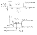
- Figure 1 is a circuit diagram of a prior art difference detector which employs operational amplifiers to eliminate any common mode voltage,
- Figure 2 is a circuit diagram of an alternative difference detector, also of the prior art, in which the voltage level of in the input signals are shifted by fixed amounts, before they are fed to a comparator,
- Figure 3 is a circuit diagram of a further alternative difference detector of the prior art which employs a current mirror technique for balanced difference detection.
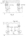
- Figure 4A and 4B are circuit diagrams of difference detectors according to the present invention, and
- Figures 5 and 6 are circuit diagrams of alternative forms of level shifting and buffering which may be included prior to the circuit of Figure 4A or 4B.
- In the circuit of Figure 1 the two input voltages VA and VB that are to be compared to see if their voltages difference exceed a certain value VREF are applied to
terminals operational amplifier 13 can be seen to ensure that its output sits at VREF + VB - VA. This feeds two furtheroperational amplifiers - The circuit of Figure 2 uses one less operational amplifier, and achieves level shifting by means of a
reference diode 20 providing a voltage offset of 2VREF. In this circuit VA, which is applied to input terminal 21, is voltage shifted by the combination of thereference diode 20 and a constantcurrent source 22 before being applied to the inverting input ofoperational amplifier 23. The unshifted voltage VA is also applied direct to the non-inverting input ofoperational amplifier 24. The voltage VB, which is applied to input terminal 25, is capacitatively coupled to the other inputs of the operational amplifiers while the two resistors R form a potential divider providing a mean voltage offset of VREF. Thusoperational amplifier 23 is turned on to provide an output atoutput terminal 26 whenever VB - VA>VREF. Similarlyoperational amplifier 24 is turned on to provide an output atoutput terminal 27 whenever V A - VB>VREF. - Although the circuit of Figure 2 uses one fewer operational amplifiers than that of Figure 1, it suffers from the disadvantage that the particular manner of obtaining a voltage offset of VREF from an offset of 2VREF means that the circuit will only handle alternating voltages. This restriction- can be avoided by deriving the requisite VREF offset in the same manner as the deriving of the 2VREF offset, but this means that the circuit requires two separate voltage offsets, one of which is exactly twice that of the other. This presents problems, particularly if it is desired to be able to adjust the magnitude of the voltage offset, for instance by replacing the reference diode with a resistor.
- The circuit of Figure 3 employs fewer transistors than either of the circuits of Figures 1 and 2. Unlike the circuit of Figure 2 it is able to operate both a.c. and d.c. with only the one voltage offset. Transistors T1 and T2 of a first amplifier circuit are connected in current mirror configuration, and also transistors T4 and T5 of a second amplifier circuit. With all resistors of equal value R, and with matched transistors, the voltage appearing at the base of T3 is VB - VA - (VREF + VD), while that at the base of T 6 is VA - V B - (VREF + VD). Therefore, if VD is equal to the base emitter voltage of transistors T3 and T6, then T3 is on whenever VB - VA VREF and similarly T6 is on whenever VA - VB vREF.
- The basic disadvantage of the circuit of Figure 3 is that the voltage that has to be input to the circuit for an offset voltage of VREF is not VREF' but VREF + VD, and hence a supply of VREF requires level shifting before it can be used in this circuit.
- The circuit of Figure 4 also uses a pair of current mirrors, these being formed respectively by transistors T7 and T8, and by transistors T10 and T11. Both resistors R of the first current mirror must be of equal value, similarly both resistors R' of the second current mirror must be of equal value. On the other hand, although it is generally preferred to choose the value of R' to be equal to that of R, this is not essential for the satisfactory operation of the difference detector. The voltage appearing at the base of transistor T9 is VD + VA - VB, whereas that appearing at the base of transistor T12 is VD + V B - VA. Therefore, transistor Tg is on whenever VA -VB>VREF while transistor T12 is on whenever VB -VA>VREF.
- For some applications there is a need to monitor only one of the two inequality relationships in which case half the circuit of Figure 4A can be dispensed with to provide the circuit of Figure 4B.
- Typically, the voltage to be compared will not be applied directly to the input terminals 40, 41 of the circuit of Figure 4A or 4B, but will first be level shifted and buffered. One piece of circuitry for this purpose is illustrated in Figure 5. Here VA and VB are respectively applied to
input terminals output terminals - An alternative to the level shifting and buffering circuit of Figure 5 is provided by the circuit of Figure 6 which has input terminals 60 and 61 and
output terminals
Claims (5)
Applications Claiming Priority (2)
| Application Number | Priority Date | Filing Date | Title |
|---|---|---|---|
| GB08413227A GB2159286B (en) | 1984-05-23 | 1984-05-23 | Voltage difference detector |
| GB8413227 | 1984-05-23 |
Publications (2)
| Publication Number | Publication Date |
|---|---|
| EP0176165A2 true EP0176165A2 (en) | 1986-04-02 |
| EP0176165A3 EP0176165A3 (en) | 1986-08-27 |
Family
ID=10561419
Family Applications (1)
| Application Number | Title | Priority Date | Filing Date |
|---|---|---|---|
| EP85302894A Withdrawn EP0176165A3 (en) | 1984-05-23 | 1985-04-25 | Voltage difference detector |
Country Status (4)
| Country | Link |
|---|---|
| EP (1) | EP0176165A3 (en) |
| JP (1) | JPS618677A (en) |
| BE (1) | BE903136R (en) |
| GB (1) | GB2159286B (en) |
Cited By (3)
| Publication number | Priority date | Publication date | Assignee | Title |
|---|---|---|---|---|
| GB2227325A (en) * | 1989-01-21 | 1990-07-25 | Ferranti Int Signal | Maximum amplitude detector |
| EP0621638A1 (en) * | 1993-04-22 | 1994-10-26 | Koninklijke Philips Electronics N.V. | Integrated high voltage differential sensor using the inverse gain of high voltage transistors |
| DE20301556U1 (en) * | 2003-02-01 | 2004-06-03 | Rosenhof, Viktor, Dr.-Ing. | Differential high voltage converter, for e.g. personal computer-controlled network quality analyzer in electrical power supply, has two identical high-resistance resistors positioned in measurement cable |
Families Citing this family (5)
| Publication number | Priority date | Publication date | Assignee | Title |
|---|---|---|---|---|
| FR2678070A1 (en) * | 1991-06-18 | 1992-12-24 | Valeo Equip Electr Moteur | CIRCUIT FOR DETECTING THE VOLTAGE BETWEEN PHASES OF AN ALTERNATOR FOR THE COMMISSIONING OF A REGULATOR ASSOCIATED WITH SUCH ALTERNATOR. |
| US7821245B2 (en) * | 2007-08-06 | 2010-10-26 | Analog Devices, Inc. | Voltage transformation circuit |
| US8362748B2 (en) | 2007-09-12 | 2013-01-29 | Rohm Co., Ltd. | Voltage comparison circuit |
| JPWO2009072281A1 (en) | 2007-12-03 | 2011-04-21 | ローム株式会社 | Power management circuit |
| JP5714274B2 (en) | 2009-10-02 | 2015-05-07 | ローム株式会社 | Semiconductor devices and electronic devices using them |
Family Cites Families (2)
| Publication number | Priority date | Publication date | Assignee | Title |
|---|---|---|---|---|
| FR2058833A5 (en) * | 1969-09-29 | 1971-05-28 | Fulmen | |
| JPS58215815A (en) * | 1982-06-09 | 1983-12-15 | Toshiba Corp | Comparator circuit |
-
1984
- 1984-05-23 GB GB08413227A patent/GB2159286B/en not_active Expired
-
1985
- 1985-04-25 EP EP85302894A patent/EP0176165A3/en not_active Withdrawn
- 1985-05-21 JP JP10919285A patent/JPS618677A/en active Pending
- 1985-08-28 BE BE2/60773A patent/BE903136R/en not_active IP Right Cessation
Cited By (6)
| Publication number | Priority date | Publication date | Assignee | Title |
|---|---|---|---|---|
| GB2227325A (en) * | 1989-01-21 | 1990-07-25 | Ferranti Int Signal | Maximum amplitude detector |
| DE4000461A1 (en) * | 1989-01-21 | 1990-07-26 | Ferranti Int Signal | DETECTOR FOR VOLTAGE DIFFERENCES |
| US5047667A (en) * | 1989-01-21 | 1991-09-10 | Gec Ferranti Defence Systems Limited | Voltage difference detector |
| GB2227325B (en) * | 1989-01-21 | 1993-06-09 | Ferranti Int Signal | Electrical detector circuits |
| EP0621638A1 (en) * | 1993-04-22 | 1994-10-26 | Koninklijke Philips Electronics N.V. | Integrated high voltage differential sensor using the inverse gain of high voltage transistors |
| DE20301556U1 (en) * | 2003-02-01 | 2004-06-03 | Rosenhof, Viktor, Dr.-Ing. | Differential high voltage converter, for e.g. personal computer-controlled network quality analyzer in electrical power supply, has two identical high-resistance resistors positioned in measurement cable |
Also Published As
| Publication number | Publication date |
|---|---|
| EP0176165A3 (en) | 1986-08-27 |
| GB2159286A (en) | 1985-11-27 |
| GB2159286B (en) | 1988-01-13 |
| JPS618677A (en) | 1986-01-16 |
| BE903136R (en) | 1986-02-28 |
| GB8413227D0 (en) | 1984-06-27 |
Similar Documents
| Publication | Publication Date | Title |
|---|---|---|
| EP0916181B1 (en) | Voltage to current converter for high frequency applications | |
| CA1093164A (en) | Biasing and scaling circuit for transducers | |
| US5231351A (en) | Magnetoresistive speed sensor processing circuit utilizing a symmetrical hysteresis signal | |
| US20060176074A1 (en) | Differential termination and attenuator network for a measurement probe having an automated common mode termination voltage generator | |
| EP0227323A2 (en) | Wideband feedback amplifier | |
| US4403183A (en) | Active voltage probe | |
| EP0176165A2 (en) | Voltage difference detector | |
| US4528499A (en) | Modified bridge circuit for measurement purposes | |
| US4445054A (en) | Full-wave rectifying circuit | |
| JP3203363B2 (en) | Peak detector | |
| JPS6232714A (en) | Offset voltage correcting circuit | |
| US4644253A (en) | Voltage reference source with true ground sensing and force-sense outputs referred thereto | |
| EP0425875A2 (en) | Full wave rectifier/averaging circuit | |
| US4294116A (en) | Temperature detecting circuit | |
| US6281717B1 (en) | Dynamic error compensation in track-and-hold circuits | |
| US6300803B1 (en) | Phase-comparison circuit | |
| US4682059A (en) | Comparator input stage for interface with signal current | |
| EP0409844B1 (en) | Amplifier arrangement and communication line circuit using same | |
| US4899064A (en) | Absolute value differential amplifier | |
| US4420698A (en) | Peak detector | |
| JPH0582087B2 (en) | ||
| US6208152B1 (en) | Redundant resistor matching detector with constant percentage threshold | |
| JP3270221B2 (en) | Optical signal receiving circuit | |
| US4530044A (en) | Self-balancing DC-substitution measuring system | |
| US4123721A (en) | Bias current compensated operational amplifier circuit |
Legal Events
| Date | Code | Title | Description |
|---|---|---|---|
| PUAI | Public reference made under article 153(3) epc to a published international application that has entered the european phase |
Free format text: ORIGINAL CODE: 0009012 |
|
| AK | Designated contracting states |
Kind code of ref document: A2 Designated state(s): AT BE CH DE FR IT LI LU NL SE |
|
| RAP1 | Party data changed (applicant data changed or rights of an application transferred) |
Owner name: STC PLC |
|
| PUAL | Search report despatched |
Free format text: ORIGINAL CODE: 0009013 |
|
| AK | Designated contracting states |
Kind code of ref document: A3 Designated state(s): AT BE CH DE FR IT LI LU NL SE |
|
| 17P | Request for examination filed |
Effective date: 19860728 |
|
| RAP1 | Party data changed (applicant data changed or rights of an application transferred) |
Owner name: STC PLC |
|
| 17Q | First examination report despatched |
Effective date: 19880504 |
|
| STAA | Information on the status of an ep patent application or granted ep patent |
Free format text: STATUS: THE APPLICATION IS DEEMED TO BE WITHDRAWN |
|
| 18D | Application deemed to be withdrawn |
Effective date: 19880915 |
|
| RIN1 | Information on inventor provided before grant (corrected) |
Inventor name: ROKOS, GEORGE HEDLEY STORM |