EP0176840A2 - Méthode et dispositif pour la détermination de position d'un capteur inductif sur une planchette - Google Patents
Méthode et dispositif pour la détermination de position d'un capteur inductif sur une planchette Download PDFInfo
- Publication number
- EP0176840A2 EP0176840A2 EP85111637A EP85111637A EP0176840A2 EP 0176840 A2 EP0176840 A2 EP 0176840A2 EP 85111637 A EP85111637 A EP 85111637A EP 85111637 A EP85111637 A EP 85111637A EP 0176840 A2 EP0176840 A2 EP 0176840A2
- Authority
- EP
- European Patent Office
- Prior art keywords
- signal
- circuit
- sensor
- inflection point
- point signal
- Prior art date
- Legal status (The legal status is an assumption and is not a legal conclusion. Google has not performed a legal analysis and makes no representation as to the accuracy of the status listed.)
- Granted
Links
Images

Classifications
-
- G—PHYSICS
- G01—MEASURING; TESTING
- G01B—MEASURING LENGTH, THICKNESS OR SIMILAR LINEAR DIMENSIONS; MEASURING ANGLES; MEASURING AREAS; MEASURING IRREGULARITIES OF SURFACES OR CONTOURS
- G01B7/00—Measuring arrangements characterised by the use of electric or magnetic techniques
- G01B7/004—Measuring arrangements characterised by the use of electric or magnetic techniques for measuring coordinates of points
Definitions
- the invention relates to a method for determining the position of an inductive sensor on a measuring table, which is provided for each coordinate with a number of current conductors arranged at fixed distances from one another.
- the current conductors are flowed through by the same currents in a predetermined sequence and direction, a measurement value used for determining the position in the relevant coordinate being generated from the measurement signal supplied by the measurement sensor.
- a method of the type mentioned at the outset is also known, in which a current signal sequence is fed to the measuring transducer and the induction signals generated by it in the current conductors are sampled and an induction signal time function is formed from these induction signals, from which a function for determining the position of the measuring transducer in of the coordinate in question is used.
- the invention has for its object to provide a method and a circuit that can be obtained with a larger G enauig- ness of the location determination and a greater independence from the height of the measuring transducer to the measuring table.
- a second derivative of the envelope curve corresponds to the time profile of the magnetic flux passing through the sensor Inflection point signal is formed and that the time interval of the second passage of this inflection point signal by a level close to zero from a reference signal started depending on the start of feeding the current conductor is used as a measure of the position of the sensor in the relevant coordinate direction.
- the solution is that an inflection point signal corresponding to the second derivative of the envelope of the induction signal time function is formed and that the distance of the second passage of this inflection point signal by a level which is close to zero is one as a function of the start the scanning of the current conductor started reference signal is used as a measure of the position of the sensor in the relevant coordinate direction.
- the time interval between the second zero crossing of the additional level and the reference signal is used as a measure of the position.
- an advantageous method variant is to be seen in that the second pass of the additional signal is determined by a level close to zero in such a way that the first Passage of the additional signal is determined by this level in the period in which the differentiated signal has an amplitude which is above a predetermined threshold.
- the circuit according to the invention is characterized in that the evaluation circuit is a comprises a second differentiating circuit to which the differentiated signal is fed and which forms a turning point signal which corresponds to the second derivative of the envelope, and also a measuring device for measuring the time distance of the second pass of the inflection point signal through a near-zero level from a reference point in time, which has a fixed time interval from the beginning of the magnetic flux pulse sequence, and that the time interval measured by the measuring device is
- the measuring device can be designed such that it measures the time interval between the second zero crossing of the turning point signal and the reference time. This measurement generally gives sufficiently accurate results.
- a particularly advantageous embodiment of a circuit can be seen in the fact that the measuring device has an enabling circuit which is controlled by the differentiated signal and is only switched through for as long; how the amplitude of the differentiated signal exceeds a certain threshold, as well as a clock, a counter for the clock pulses of the clock, a starting circuit, which is in a fixed The time interval from the start of the generation of the magnetic flux pulses enables the clock pulses to the counter, by a discriminator circuit which generates a stop signal for the counter each time the turning point signal passes a predetermined, near-zero level and when the enable circuit is switched on, and an indicator - Or storage device for the count value.
- the discriminator circuit can be designed so that a stop signal is generated at the zero crossing of the turning point signal. This stop signal is not effective at the first zero crossing, since the enable circuit has not yet been enabled and the counter therefore continues to count.
- An increase in measuring accuracy can be achieved in that the discriminator circuit is designed such that a stop signal is generated when the turning point signal is the same as a signal fluctuating synchronously with the activation of the current conductors.
- the differentiating circuits can be designed as bandpasses. This has the advantage that the noise and interference signals are reduced.
- the threshold value is set to a value between 10 and 60% of the maximum of the second half-wave of the differentiated signal.
- the circuit shown in Fig. 1 for measuring the position of the sensor on the measuring table in a coordinate receives from the winding 1 of a sensor on line 2 a measurement signal, the size of which is determined by the change in time of the magnetic flux flowing through the winding 1.
- This magnetic flux is generated by the grid lines of a measuring table which are assigned to the relevant coordinate direction and are arranged in parallel and at a distance from one another and through which current pulses flow in a predetermined sequence.
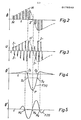
- the cross-sectional area of the winding 1 is therefore penetrated by a magnetic flux, which is shown in Fig. 2.
- the magnetic flux 4 generated by the current flow in the individual grid lines is plotted as a function of time.
- the duration of the magnetic flux is equal to the duration of the current flow, and the magnitude of the magnetic flux depends on the distance of the measuring transducer containing the winding 1 from the grid line through which current flows. It can be seen that the magnetic flux increases gradually and passes through 0 after a maximum at point Z has been exceeded. This zero crossing of the magnetic flux corresponds to a position of the sensor on the measuring table, at which the electrical center of the winding 1 is symmetrical to the grid lines.
- Magnetic flux pulses M generate a voltage pulse I + of one polarity through the rising edge and a voltage pulse I- of the same magnitude but opposite polarity through the falling edge.
- a sample and hold circuit sample memory circuit
- the measurement signal passes from the winding 1 via the line 2 to the sample and hold circuit 3, at the output of which a series of pulses occur, the level of which is equal to the voltage pulses I + of Fig. 3, the thus practically correspond to the height of the magnetic flux pulses M, the width of which, however, extends to the beginning of the next pulse, as indicated in FIG. 3 by dotted lines.
- a low-pass filter 4 the cut-off frequency of which is lower than the repetition rate of the magnetic flux pulses M, is used to smooth this voltage curve. At the output of the low-pass filter 4, a voltage thus results which corresponds to the envelope curve H shown in FIG.
- a bandpass filter is connected to the output of the low pass 4, which comprises an operational amplifier 5, the N input of which is connected on the one hand via the series circuit of a resistor 6 and a capacitor 7 to the output of the low pass 4 and on the other hand via the parallel connection of a resistor 8 and one Capacitor 9 with its own output.
- the size of the resistors 6 and 8 and the capacitors 7 and 9 such a bandpass has a slope of 6 db up to a maximum angular frequency, which is significantly smaller than the reciprocal of the time constant from the Resistor 6 and capacitor 7.
- the time constant of resistor 8 in connection with capacitor 9 can be of the same size.
- the differentiated signal has two zero crossings, namely a first zero crossing O 1 , which is temporally at the location of the first maximum of the envelope curve H of Fig. 2, and a second zero crossing 0 2 , which coincides with time the second maximum of the envelope curve H coincides. Between these two zero crossings, the differentiated signal has a profile that resembles a half wave of a sine wave. The maximum P of this signal section coincides with the turning point of the envelope curve H in time.
- a second bandpass filter 17 is connected to the output 10 of the bandpass filter 11 and is formed from an operational amplifier 12, the series connection of a resistor 13 and a capacitor 14 and the parallel connection of a resistor 15 and a capacitor 16, these parts being connected in the same way are like bandpass 11.
- a voltage occurs at the output 18 of the second band pass 17, the course of which is shown in FIG. 5.
- This voltage f "(t) forms the second derivative of the envelope curve H and has three zero crossings, which are designated in turn with N 1 , N 2 and N 3. These zero crossings correspond in time to the three maxima of the differentiated signal (FIG. 4 ).
- the output 10 of the bandpass filter 11, at which the differentiated signal occurs, is connected via a resistor 19 to the N input of a differential amplifier 20, the P input of which is connected via a resistor 21 to a voltage source U which has a specific threshold value S is set.
- a pair of anti-parallel diodes 22 and 23 are connected in parallel to the inputs of the differential amplifier 20.
- the assembly consisting of parts 19 to 23 forms a voltage comparator, at the output 24 of which an output signal, for example an H level, occurs only as long as the output 10 is at a level which is more negative than the threshold value S.
- an output signal for example an H level
- the output 24 of the voltage comparator 19-23 is connected to an input of an AND gate 25.
- This AND gate is part of the stop circuit.
- the circuit further includes a clock 26 which is connected to the one input of an AND gate 42.
- a start circuit 27 is also provided, which forms a monostable multivibrator, the output of which is connected to the second input of the AND gate 42.
- the input 28 of the start circuit 27 is connected via a capacitor 29 to the supply circuit for the grid lines, also called current conductors.
- the output 18 of the second bandpass 17 is connected to a discriminator circuit which is designed as a voltage comparator and comprises a differential amplifier 30, each having a resistor 31 and 32 connected to the inputs and two diodes 33 and 34 connected in antiparallel and parallel to the input.
- the output 18 is connected via the resistor 32 to the P input of the differential amplifier, and the N input thereof leads via the resistor 31 to the Grinder of a potentiometer 35, the end connections of which are connected to a negative or positive voltage, so that a voltage in the range around the zero point can be set.
- an AC voltage component U is also fed to the N input of the differential amplifier 30 via the resistor 44, which changes synchronously with the clock frequency of the magnetic field pulses and which serves to fine-tune the measurement error caused by the mutual finite distance between the current conductors.
- the output of the discriminator circuit 37 consisting of the parts 30 to 34 is connected via a capacitor 36 to the second input of the AND gate 25, the output of which is connected to the reset input 38 of a binary counter 39.
- a display and / or storage device 41 is provided which, when a reset signal is received on line 38, takes over the count value digitally present at the outputs Q1 to Qn of the counter 39 into a memory.
- the circuit works as follows.
- This signal is differentiated by the rising edge of the bandpass 11, so that a differentiated signal corresponding to FIG. 4 occurs at the output 10 of this bandpass.
- This differentiated signal arrives at the N input of the differential amplifier 20 and leads to an H level at the output 24 of the differential amplifier 20 only if the differentiated voltage is more negative than the threshold voltage U s , which is shown in broken lines in FIG. 4.
- the AND gate 25 is transparent to signals at the second input.
- the differentiated signal present at the output 10 is differentiated via the second bandpass filter 17, so that a turning point signal occurs at the output thereof which corresponds to the second derivative of the envelope curve H, H '.
- This signal is shown in FIG. 5.
- the differential amplifier 30 whose N input is set to a voltage equal to or close to zero, the output level of this differential amplifier switches every time the voltage at the output 18 passes through this level. These switching points are shown in Fig. 5 with N i . N 2 and N 3 designated.
- the level present at the N input of the differential amplifier 30 is shown in broken lines in FIG. 5 (without an AC voltage component).
- the pulse duration of the monostable multivibrator in the start circuit 27 is selected to be greater than the time interval between two successive pulses on line 2. This ensures that the start circuit 27 has an H level at the output 43 as long as the grid lines are supplied with current .
- clock signals from the clock generator 28 also reach the counting input 40 of the binary counter 39 through the AND gate 42.
- the start of the power supply to the grid line can also be controlled or synchronized by the clock generator 26, it also being possible to carry out a certain time delay or advance the power supply compared to the clock signals, for example to correct certain circuit properties.
- the binary counter 39 is started when the first signal occurs at the input 28 of the start circuit 27, and the counter stops counting and is reset at the same time when the AND gate 25 corresponds to a level crossing N 2 in FIG. 5 Pass pulse from the differential amplifier 30.
- the magnetic field pulses can also be generated with the sensor, in which case the induction voltage is then scanned one after the other by the current conductors.
- the circuit described above can also be used for this purpose, the line circuit containing the current conductors then being connected to line 2 instead of measuring coil 1.
Landscapes
- Physics & Mathematics (AREA)
- General Physics & Mathematics (AREA)
- Measurement Of Length, Angles, Or The Like Using Electric Or Magnetic Means (AREA)
Applications Claiming Priority (2)
| Application Number | Priority Date | Filing Date | Title |
|---|---|---|---|
| DE3436639 | 1984-10-05 | ||
| DE19843436639 DE3436639A1 (de) | 1984-10-05 | 1984-10-05 | Verfahren und vorrichtung zur positionsbestimmung eines induktiven messaufnehmers auf einem messtisch |
Publications (3)
| Publication Number | Publication Date |
|---|---|
| EP0176840A2 true EP0176840A2 (fr) | 1986-04-09 |
| EP0176840A3 EP0176840A3 (en) | 1989-06-21 |
| EP0176840B1 EP0176840B1 (fr) | 1991-06-12 |
Family
ID=6247226
Family Applications (1)
| Application Number | Title | Priority Date | Filing Date |
|---|---|---|---|
| EP85111637A Expired - Lifetime EP0176840B1 (fr) | 1984-10-05 | 1985-09-14 | Méthode et dispositif pour la détermination de position d'un capteur inductif sur une planchette |
Country Status (3)
| Country | Link |
|---|---|
| EP (1) | EP0176840B1 (fr) |
| JP (1) | JPH0619695B2 (fr) |
| DE (2) | DE3436639A1 (fr) |
Families Citing this family (3)
| Publication number | Priority date | Publication date | Assignee | Title |
|---|---|---|---|---|
| JP3061404B2 (ja) * | 1990-09-13 | 2000-07-10 | シャープ株式会社 | ディスプレイ一体型タブレット |
| DE4307453A1 (de) * | 1993-03-10 | 1994-09-15 | Ruhrgas Ag | Verfahren und Vorrichtung zum Orten einer Leitung |
| DE19522697A1 (de) * | 1995-06-22 | 1997-01-09 | Sick Optik Elektronik Erwin | Verfahren und Schaltungsanordnung zur Messung der Strömungsgeschwindigkeit mittels akustischer Laufzeitdifferenzen |
Family Cites Families (5)
| Publication number | Priority date | Publication date | Assignee | Title |
|---|---|---|---|---|
| JPS5416207A (en) * | 1977-07-07 | 1979-02-06 | Yoshio Shimada | Original holder for plate making machine |
| US4514688A (en) * | 1980-06-23 | 1985-04-30 | Summagraphics Corporation | Digital tablet system with calibration means |
| DE3243712A1 (de) * | 1982-11-25 | 1984-05-30 | Preh Elektro Feinmechanik | Einrichtung zur erfassung einer x-y-position |
| DE3402905A1 (de) * | 1983-03-08 | 1984-09-13 | Robotron Veb K | Koordinatenbestimmungsvorrichtung, insbesondere fuer genau messende digitalisiergeraete |
| JPS617917A (ja) * | 1984-06-22 | 1986-01-14 | Nec Corp | 座標入力装置 |
-
1984
- 1984-10-05 DE DE19843436639 patent/DE3436639A1/de not_active Withdrawn
-
1985
- 1985-09-14 EP EP85111637A patent/EP0176840B1/fr not_active Expired - Lifetime
- 1985-09-14 DE DE8585111637T patent/DE3583199D1/de not_active Expired - Lifetime
- 1985-10-04 JP JP60221722A patent/JPH0619695B2/ja not_active Expired - Lifetime
Also Published As
| Publication number | Publication date |
|---|---|
| DE3583199D1 (de) | 1991-07-18 |
| DE3436639A1 (de) | 1986-04-10 |
| JPS61172001A (ja) | 1986-08-02 |
| EP0176840A3 (en) | 1989-06-21 |
| EP0176840B1 (fr) | 1991-06-12 |
| JPH0619695B2 (ja) | 1994-03-16 |
Similar Documents
| Publication | Publication Date | Title |
|---|---|---|
| DE2816981A1 (de) | Einrichtung zur messung der gleichstromkomponente in einem ueberlagerten wechselspannungssignal | |
| EP0065762B1 (fr) | Méthode et arrangement de circuit pour mesurer un champ magnétique, spécialement le champ magnétique terrestre | |
| DE3106396A1 (de) | Wandler, insbesondere analog-zu-digital-wandler fuer einen elektromagnetischen stroemungsmesser | |
| DE2421824A1 (de) | Verfahren und vorrichtung zur feststellung der mittelamplitude von impulsen bei der teilchenuntersuchung | |
| EP0176840B1 (fr) | Méthode et dispositif pour la détermination de position d'un capteur inductif sur une planchette | |
| DE2156766C3 (de) | ImpulsdauermeBvorrichtung | |
| DE2362312B2 (de) | Gepulstes Wirbelstrom-Prüfgerät | |
| DE2917788A1 (de) | Materialpruefgeraet | |
| DE3529591A1 (de) | Verfahren und vorrichtung zum betrieb eines wechselrichters | |
| DE2144537C3 (de) | Meldeanlage | |
| DE3826551C2 (de) | Vorrichtung zur Leistungsfaktormessung | |
| DE2834499C2 (de) | Schaltungsanordnung zum potentialfreien Messen von Strömen oder Spannungen | |
| DE1772633A1 (de) | Verfahren zur Spracherkennung | |
| DE2203963C3 (de) | Schaltungsanordnung zur Verarbeitung von elektrischen Signalen | |
| DE2547746A1 (de) | Vorrichtung mit einer messwertgeber-einheit zur erzeugung einer folge von spannungswerten und einer mittelwertbildungs-einheit | |
| DE2550060A1 (de) | Verfahren und einrichtung zur detektion einer vormagnetisierung | |
| DE4211430C1 (de) | Schaltungsanordnung zur Erzeugung eines zeitvariablen Ausgangssignals | |
| DE964427C (de) | Verfahren zur Messung des Phasenwinkels zwischen zwei Wechselspannungen | |
| DE1523161C (de) | Anordnung zur Messung der Relativ geschwindigkeit eines Fluids | |
| DE3232425A1 (de) | Verwendung eines elektronischen empfaengers mit differentialtransformator zum messen der augenblicksgeschwindigkeit und/oder der augenblicklichen aenderung der geschwindigkeit eines beweglichen koerpers zusammen mit der messung seiner lage | |
| DE3422805C1 (de) | Schaltungsanordnung zur Messung der Zeitdifferenz zwischen Impulsen | |
| DE1623261A1 (de) | Vorrichtung zur Bestimmung der Groesse und des Vorzeichens eines Frequenzunterschiedes | |
| DE2720023A1 (de) | Schaltungsanordnung zur messung der reziproken frequenz einer wechselspannung | |
| DE3511864A1 (de) | Koordinatenmessvorrichtung | |
| DE4309792A1 (de) | Vereinfachte Erfassung von Wechselgrößen |
Legal Events
| Date | Code | Title | Description |
|---|---|---|---|
| PUAI | Public reference made under article 153(3) epc to a published international application that has entered the european phase |
Free format text: ORIGINAL CODE: 0009012 |
|
| 17P | Request for examination filed |
Effective date: 19850914 |
|
| AK | Designated contracting states |
Kind code of ref document: A2 Designated state(s): CH DE FR GB IT LI |
|
| PUAL | Search report despatched |
Free format text: ORIGINAL CODE: 0009013 |
|
| AK | Designated contracting states |
Kind code of ref document: A3 Designated state(s): CH DE FR GB IT LI |
|
| RAP1 | Party data changed (applicant data changed or rights of an application transferred) |
Owner name: KONTRON ELEKTRONIK GMBH |
|
| 17Q | First examination report despatched |
Effective date: 19900514 |
|
| GRAA | (expected) grant |
Free format text: ORIGINAL CODE: 0009210 |
|
| AK | Designated contracting states |
Kind code of ref document: B1 Designated state(s): CH DE FR GB IT LI |
|
| GBT | Gb: translation of ep patent filed (gb section 77(6)(a)/1977) | ||
| REF | Corresponds to: |
Ref document number: 3583199 Country of ref document: DE Date of ref document: 19910718 |
|
| ET | Fr: translation filed | ||
| ITF | It: translation for a ep patent filed | ||
| PLBE | No opposition filed within time limit |
Free format text: ORIGINAL CODE: 0009261 |
|
| STAA | Information on the status of an ep patent application or granted ep patent |
Free format text: STATUS: NO OPPOSITION FILED WITHIN TIME LIMIT |
|
| 26N | No opposition filed | ||
| PGFP | Annual fee paid to national office [announced via postgrant information from national office to epo] |
Ref country code: GB Payment date: 19970908 Year of fee payment: 13 |
|
| PGFP | Annual fee paid to national office [announced via postgrant information from national office to epo] |
Ref country code: CH Payment date: 19970911 Year of fee payment: 13 |
|
| PGFP | Annual fee paid to national office [announced via postgrant information from national office to epo] |
Ref country code: DE Payment date: 19970925 Year of fee payment: 13 |
|
| PGFP | Annual fee paid to national office [announced via postgrant information from national office to epo] |
Ref country code: FR Payment date: 19970929 Year of fee payment: 13 |
|
| PG25 | Lapsed in a contracting state [announced via postgrant information from national office to epo] |
Ref country code: GB Free format text: LAPSE BECAUSE OF NON-PAYMENT OF DUE FEES Effective date: 19980914 |
|
| PG25 | Lapsed in a contracting state [announced via postgrant information from national office to epo] |
Ref country code: LI Free format text: LAPSE BECAUSE OF NON-PAYMENT OF DUE FEES Effective date: 19980930 Ref country code: CH Free format text: LAPSE BECAUSE OF NON-PAYMENT OF DUE FEES Effective date: 19980930 |
|
| GBPC | Gb: european patent ceased through non-payment of renewal fee |
Effective date: 19980914 |
|
| REG | Reference to a national code |
Ref country code: CH Ref legal event code: PL |
|
| PG25 | Lapsed in a contracting state [announced via postgrant information from national office to epo] |
Ref country code: FR Free format text: LAPSE BECAUSE OF NON-PAYMENT OF DUE FEES Effective date: 19990531 |
|
| PG25 | Lapsed in a contracting state [announced via postgrant information from national office to epo] |
Ref country code: DE Free format text: LAPSE BECAUSE OF NON-PAYMENT OF DUE FEES Effective date: 19990701 |
|
| REG | Reference to a national code |
Ref country code: FR Ref legal event code: ST |