EP0178181A2 - Verfahren zur Herstellung einer Öffnung in einem Substrat - Google Patents
Verfahren zur Herstellung einer Öffnung in einem Substrat Download PDFInfo
- Publication number
- EP0178181A2 EP0178181A2 EP85307301A EP85307301A EP0178181A2 EP 0178181 A2 EP0178181 A2 EP 0178181A2 EP 85307301 A EP85307301 A EP 85307301A EP 85307301 A EP85307301 A EP 85307301A EP 0178181 A2 EP0178181 A2 EP 0178181A2
- Authority
- EP
- European Patent Office
- Prior art keywords
- layer
- metal
- exposed
- aperture
- gate
- Prior art date
- Legal status (The legal status is an assumption and is not a legal conclusion. Google has not performed a legal analysis and makes no representation as to the accuracy of the status listed.)
- Withdrawn
Links
Images

Classifications
-
- H—ELECTRICITY
- H10—SEMICONDUCTOR DEVICES; ELECTRIC SOLID-STATE DEVICES NOT OTHERWISE PROVIDED FOR
- H10D—INORGANIC ELECTRIC SEMICONDUCTOR DEVICES
- H10D30/00—Field-effect transistors [FET]
- H10D30/01—Manufacture or treatment
- H10D30/061—Manufacture or treatment of FETs having Schottky gates
- H10D30/0612—Manufacture or treatment of FETs having Schottky gates of lateral single-gate Schottky FETs
- H10D30/0614—Manufacture or treatment of FETs having Schottky gates of lateral single-gate Schottky FETs using processes wherein the final gate is made after the completion of the source and drain regions, e.g. gate-last processes using dummy gates
-
- G—PHYSICS
- G03—PHOTOGRAPHY; CINEMATOGRAPHY; ANALOGOUS TECHNIQUES USING WAVES OTHER THAN OPTICAL WAVES; ELECTROGRAPHY; HOLOGRAPHY
- G03F—PHOTOMECHANICAL PRODUCTION OF TEXTURED OR PATTERNED SURFACES, e.g. FOR PRINTING, FOR PROCESSING OF SEMICONDUCTOR DEVICES; MATERIALS THEREFOR; ORIGINALS THEREFOR; APPARATUS SPECIALLY ADAPTED THEREFOR
- G03F7/00—Photomechanical, e.g. photolithographic, production of textured or patterned surfaces, e.g. printing surfaces; Materials therefor, e.g. comprising photoresists; Apparatus specially adapted therefor
- G03F7/26—Processing photosensitive materials; Apparatus therefor
- G03F7/40—Treatment after imagewise removal, e.g. baking
-
- H—ELECTRICITY
- H10—SEMICONDUCTOR DEVICES; ELECTRIC SOLID-STATE DEVICES NOT OTHERWISE PROVIDED FOR
- H10P—GENERIC PROCESSES OR APPARATUS FOR THE MANUFACTURE OR TREATMENT OF DEVICES COVERED BY CLASS H10
- H10P76/00—Manufacture or treatment of masks on semiconductor bodies, e.g. by lithography or photolithography
- H10P76/40—Manufacture or treatment of masks on semiconductor bodies, e.g. by lithography or photolithography of masks comprising inorganic materials
- H10P76/405—Manufacture or treatment of masks on semiconductor bodies, e.g. by lithography or photolithography of masks comprising inorganic materials characterised by their composition, e.g. multilayer masks
-
- H—ELECTRICITY
- H10—SEMICONDUCTOR DEVICES; ELECTRIC SOLID-STATE DEVICES NOT OTHERWISE PROVIDED FOR
- H10P—GENERIC PROCESSES OR APPARATUS FOR THE MANUFACTURE OR TREATMENT OF DEVICES COVERED BY CLASS H10
- H10P76/00—Manufacture or treatment of masks on semiconductor bodies, e.g. by lithography or photolithography
- H10P76/40—Manufacture or treatment of masks on semiconductor bodies, e.g. by lithography or photolithography of masks comprising inorganic materials
- H10P76/408—Manufacture or treatment of masks on semiconductor bodies, e.g. by lithography or photolithography of masks comprising inorganic materials characterised by their sizes, orientations, dispositions, behaviours or shapes
- H10P76/4085—Manufacture or treatment of masks on semiconductor bodies, e.g. by lithography or photolithography of masks comprising inorganic materials characterised by their sizes, orientations, dispositions, behaviours or shapes characterised by the processes involved to create the masks
-
- Y—GENERAL TAGGING OF NEW TECHNOLOGICAL DEVELOPMENTS; GENERAL TAGGING OF CROSS-SECTIONAL TECHNOLOGIES SPANNING OVER SEVERAL SECTIONS OF THE IPC; TECHNICAL SUBJECTS COVERED BY FORMER USPC CROSS-REFERENCE ART COLLECTIONS [XRACs] AND DIGESTS
- Y10—TECHNICAL SUBJECTS COVERED BY FORMER USPC
- Y10S—TECHNICAL SUBJECTS COVERED BY FORMER USPC CROSS-REFERENCE ART COLLECTIONS [XRACs] AND DIGESTS
- Y10S148/00—Metal treatment
- Y10S148/105—Masks, metal
-
- Y—GENERAL TAGGING OF NEW TECHNOLOGICAL DEVELOPMENTS; GENERAL TAGGING OF CROSS-SECTIONAL TECHNOLOGIES SPANNING OVER SEVERAL SECTIONS OF THE IPC; TECHNICAL SUBJECTS COVERED BY FORMER USPC CROSS-REFERENCE ART COLLECTIONS [XRACs] AND DIGESTS
- Y10—TECHNICAL SUBJECTS COVERED BY FORMER USPC
- Y10S—TECHNICAL SUBJECTS COVERED BY FORMER USPC CROSS-REFERENCE ART COLLECTIONS [XRACs] AND DIGESTS
- Y10S148/00—Metal treatment
- Y10S148/111—Narrow masking
-
- Y—GENERAL TAGGING OF NEW TECHNOLOGICAL DEVELOPMENTS; GENERAL TAGGING OF CROSS-SECTIONAL TECHNOLOGIES SPANNING OVER SEVERAL SECTIONS OF THE IPC; TECHNICAL SUBJECTS COVERED BY FORMER USPC CROSS-REFERENCE ART COLLECTIONS [XRACs] AND DIGESTS
- Y10—TECHNICAL SUBJECTS COVERED BY FORMER USPC
- Y10S—TECHNICAL SUBJECTS COVERED BY FORMER USPC CROSS-REFERENCE ART COLLECTIONS [XRACs] AND DIGESTS
- Y10S438/00—Semiconductor device manufacturing: process
- Y10S438/942—Masking
- Y10S438/947—Subphotolithographic processing
Definitions
- the subject matter of the present invention relates to methods for producing an aperture in a surface, and particularly, but not exclusively, to methods for obtaining apertures of sublithographic dimension in the manufacture of integrated circuits, and especially submicron apertures for defining the gate lengths of transistors for high speed operation.
- a critical element in the development of fast operating transistors and integrated circuits is the minimum gate length that these devices may be given. Determination of that gate length will often rest upon the minimum dimension that may be etched through a dielectric layer to an underlying substrate.
- a photoresist layer is placed above the dielectric layer and is then masked in the desired pattern. After exposure to radiation, either the exposed or the unexposed portions of that resist are removed. Through the apertures so created, portions of the underlying dielectric layer corresponding to the pattern of the original photolithographic mask are removed by etching.
- the minimum linear dimension that can be created in that fashion using optical radiation is on the order of one micrometer (pm).
- Half micrometer lithography is occasionally achieved, but with reduced yield and uniformity.
- An "edge-plating" process described in IEEE IEDM Sect. 3.6, Sept. 1979, pp. 58-61, also uses a two-metal double layer to place the gate directly on the substrate, but in this case portions of the upper metal are first removed. The edges of the upper metal so exposed are then plated with a third metal which serves as a mask in removing a portion of the original double layers. The lower metal protected by such mask then remains to serve as the gate.
- the special steps employed in this edge-plating process include the use of special mask sets in a separate gate metallization step.
- directional evaporation of the gate metal is employed, so that rotation of the substrate is prohibited. Formation of the wider interconnect lines and the gate recess process must also be performed separately from the gate metallization. It is also difficult to control the gate dimension when etching away the original metal.
- U .S. Patent No. 4,389,768 to Fowler et al discloses a structure comprising a lightly doped layer in source, drain and channel regions, above that more heavily doped mesas in source and drain regions only, and above that a dielectric covering.
- the channel space between the mesas may be defined at the photolithographic limit.
- Directional reactive ion etching then removes some of the dielectric over this channel space, thereby defining a gate region of a smaller dimension and leaving dielectric sidewalls on the mesas.
- Source and drain regions are formed by thermal diffusion from the mesas into the lower region, including some lateral diffusion into the channel under the sidewalls.
- the channel length will generally be greater than the gate length, since the lateral diffusion cannot be precisely controlled.
- subrnicron apertures are formed in a dielectric substrate by a complex series of depositions, thermal oxidations, and etching of selected dielectric layers.
- the invention may be used to permit fabrication of submicron apertures in a substrate for purposes of manufacturing high speed transistors and integrated circuits and for other application.
- the invention may further be used to exceed the lithographic limits in the minimum dimension of such apertures, but in a way that will not require expensive special equipment or process steps, so that departures from conventional manufacturing processes will be minimized.
- a dielectric layer overlying a substrate is first formed.
- a metal film is deposited onto the dielectric layer followed by a photoresist layer which is masked, exposed and developed to generate appropriate photoresist images.
- the metal film is then etched to expose the underlying dielectric in a pattern established by the image.
- the portions of metal film abutting the gap so created are then subjected to controlled electrodeposition of additional metal, thus decreasing the area of the exposed dielectric.
- Etching of the underlying dielectric then defines an aperture or gate length that is likewise smaller than the lithographic limit.
- the remaining steps of manufacture may be entirely conventional, or special gate metallization techniques may be employed, but in either case a self-aligned gate structure of sublithographic dimension will be achieved.
- Figures 1-5 illustrate the successive steps of carrying out the process of the present invention in the particular case of a GaAs transistor device.
- Fig. 1 shows an initial structure that is appropriate for such purpose, and then the succeeding figures lead to the final product shown in Fig. 5.
- a method embodying the invention is employed in processes for creating apertures in a surface, or in added layers overlying such a surface, and particularly as an adjunct to conventional photolithography.
- a surface may be the surface of a structure such as that shown in Fig. 1 where there appear transistor elements such as source and drain regions, and the invention then serves to create gate elements that are shorter than conventional photolithography permits.
- Fig. 1 illustrates a substrate 10 formed from an undoped GaAs wafer grown by the liquid encapsulated Czochralski (LEC) method. This method has been described in M. Nowogradski, Ed., Advanced III-V Semiconductor Materials Technology Assessment, Noyes Publications, Park Ridge, N.J., 1984, pp. 25-33.
- a 100 nm SiO 2 layer (not shown) is formed on a cleaned major surface of substrate 10 by chemical vapor deposition (CVD).
- Masked photoresist layers are used to define areas for regions 11 which will constitute the n+ source and drain elements, and an area for the n- channel region 12 which interconnects regions 11.
- Silicon is then ion-implanted into the substrate 10 throughout regions 11 and 12 to a concentration of about 2 - 3 X 10 17 cm -3 .
- a second masking is then used to allow ion-implantation of silicon into the n+ regions 11 only, to a concentration of approximately 3 X 10 18 cm -3 .
- a second 100 nm layer of Si0 2 (not shown) is formed by CVD to serve as an anneal cap. Annealing is then carried out at about 800 °C. In order to carry out the remaining steps, all of the Si0 2 is then removed.
- a 100 nm layer of silicon nitride (Si N 4 ) is then applied by sputtering, and photolithographic masking and etching are again used to give access to regions 11 only. Above regions 11, a Au-Ge-Ni alloy is deposited by electron beam evaporation to form ohmic contacts 13. After removing the photoresist material, an additional 100 nm of Si 3 N 4 is applied to the entire surface to form the dielectric layer 14 and complete the structure of Fig. 1.
- metal film 15 is employed over the entire surface of dielectric layer 14.
- metal film 15 there is first deposited 5 nm of Ti, then 50 nm of Au, and then another 10 nm of Ti.
- a photoresist layer 16 is then deposited over all of metal film 15 and masked to define an area for gate aperture 17.
- Plasma and/or wet chemical etching of metal film 15 down to the dielectric layer 14 then form gate aperture 17.
- gate aperture 17 can be given a minimum dimension of about 1 micrometer. The etching which produces aperture 17 then completes the structure of Fig. 2.
- Electrolytic deposition is then employed to deposit nickel on the edges of the film 15 that are exposed at the boundary of the aperture 17. This is accomplished by placing the structure of Fig. 2 and a sheet of Ni in an electrolytic solution containing nickel ions, with the metal film 15 and the sheet of Ni connected to a d.c. voltage source as cathode and anode respectively. Connection is made to the metal film 15 at the periphery of the wafer.
- a secondary cathode, comprising a sheet of Ni having a surface area many times the exposed area of the metal film 15, is also connected to the voltage source and is immersed in the electrolytic solution, thus avoiding any extremes in current density which could occur if the exposed areas of the metal film 15 were the only cathode surface.
- the electrolytic solution should comprise an acidic, aqueous solution of nickel sulfate prepared from commercially available electrolyte formulations (Watts-type nickel bath), with the concentration of nickel sulfate in the range from 250 - 330 g/l.
- the concentration of nickel sulfate in the range from 250 - 330 g/l.
- Proper deposition will then occur using a current of 100 mA at 6 v for approximately 45 seconds. In order to obtain a deposit of uniform thickness, deposition takes place at a temperature of 44°C.
- Fig. 3 shows the regions of electrodeposited nickel 18 that result from the electrodeposition process and bound an aperture region 17' which is reduced in size compared to the aperture 17.
- the metal regions 18 so formed then provide additional masking and reduce the area of the layer 14 that is exposed.
- a plasma enhanced chemical etch of the underlying dielectric 14 then yields gate region 19.
- the photoresist layer 16, metal film 15, and the metal regions 18 are then removed by selective solvents and chemical etches in a conventional manner.
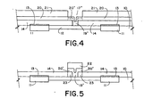
- Fig. 4 then illustrates the gate metallization procedure employed in this preferred embodiment.
- a metal layer 20 is formed by sputtering first 70 nm of TiW, then 40 nm of Pd, and finally another 20 nm of Tiw.
- gate region 19 becomes filled with metal to become the actual gate element 19'.
- Photoresist layer 21 is then applied and is masked using the same mask as was employed in creating gate aperture 17. Layer 21 is exposed and the photoresist is removed to define an aperture 17" of the same size, shape and position as the gate aperture 17.
- the top 20 nm of TiW is etched out through the aperture 17" to expose a clean surface of Pd.
- the remaining metal of the layer 20 that is exposed through the aperture 17" makes up a premetallization layer 20' shown below the dashed line in Fig. 4.
- gate lengths measured in the range from 0.5 to 0.3 pin have been obtained. This compares favorably to the minimum gate length of 1 pin that is normally obtainable using conventional photolithography.
- a gate recess so obtained would be self-aligned to the gate metal and would have dimensions commensurate with the reduced gate length. That is significant from the point of view of seeking increased device performance.
- the single device described is of course intended to represent a plurality of such devices on a single wafer or group of wafers.
- the use of a three-state metal film 15 is helpful for the electrodeposition which will follow, but it should be understood that the metals actually employed are only required to be electrically conducting and susceptible to an even electrodeposition thereon, and their precise dimensions may also be varied.
- metal films of sputtered TiW and evaporated copper have also been employed.
- the first and second layers need only be substantially coextensive in the vicinity of the aperture that they define, their relative extent away from the aperture being irrelevant to the invention.
- references in the claims to a body or member being of dielectric material are intended to be taken in the context in which they are presented, namely, relative to a metal or other conductive material in an electrodeposition process. It is necessary only that the resistivity of the dielectric material be sufficient that the metal that is electrodeposited be deposited on the conductive material rather than the dielectric material.
Landscapes
- Physics & Mathematics (AREA)
- General Physics & Mathematics (AREA)
- Junction Field-Effect Transistors (AREA)
- Electrodes Of Semiconductors (AREA)
- Drying Of Semiconductors (AREA)
Applications Claiming Priority (2)
| Application Number | Priority Date | Filing Date | Title |
|---|---|---|---|
| US06/660,172 US4759822A (en) | 1984-10-12 | 1984-10-12 | Methods for producing an aperture in a surface |
| US660172 | 1984-10-12 |
Publications (2)
| Publication Number | Publication Date |
|---|---|
| EP0178181A2 true EP0178181A2 (de) | 1986-04-16 |
| EP0178181A3 EP0178181A3 (de) | 1987-08-19 |
Family
ID=24648458
Family Applications (1)
| Application Number | Title | Priority Date | Filing Date |
|---|---|---|---|
| EP85307301A Withdrawn EP0178181A3 (de) | 1984-10-12 | 1985-10-11 | Verfahren zur Herstellung einer Öffnung in einem Substrat |
Country Status (3)
| Country | Link |
|---|---|
| US (1) | US4759822A (de) |
| EP (1) | EP0178181A3 (de) |
| JP (1) | JPS61105845A (de) |
Cited By (1)
| Publication number | Priority date | Publication date | Assignee | Title |
|---|---|---|---|---|
| EP0409681A1 (de) * | 1989-07-21 | 1991-01-23 | Thomson Composants Microondes | Verfahren zur Herstellung von extrem feinen Gittern |
Families Citing this family (10)
| Publication number | Priority date | Publication date | Assignee | Title |
|---|---|---|---|---|
| KR880009419A (ko) * | 1987-01-26 | 1988-09-15 | 이찌하라 시로 | 반도체소자의 제조방법 및 그 방법에 의해 제조된 반도체 소자 |
| JP2508818B2 (ja) * | 1988-10-03 | 1996-06-19 | 三菱電機株式会社 | 半導体装置の製造方法 |
| US5118382A (en) * | 1990-08-10 | 1992-06-02 | Ibm Corporation | Elimination of etch stop undercut |
| US5420067A (en) * | 1990-09-28 | 1995-05-30 | The United States Of America As Represented By The Secretary Of The Navy | Method of fabricatring sub-half-micron trenches and holes |
| EP0645621A3 (de) * | 1993-09-28 | 1995-11-08 | Siemens Ag | Sensoranordnung. |
| US5776836A (en) * | 1996-02-29 | 1998-07-07 | Micron Technology, Inc. | Self aligned method to define features smaller than the resolution limit of a photolithography system |
| WO1998036107A1 (en) * | 1997-02-14 | 1998-08-20 | Dover Industrial Chrome, Inc. | Plating apparatus and method |
| US5920102A (en) * | 1997-05-30 | 1999-07-06 | Motorola, Inc. | Semiconductor device having a decoupling capacitor and method of making |
| US6489237B1 (en) | 2001-12-04 | 2002-12-03 | Taiwan Semiconductor Manufacturing Company | Method of patterning lines in semiconductor devices |
| US7585424B2 (en) * | 2005-01-18 | 2009-09-08 | Hewlett-Packard Development Company, L.P. | Pattern reversal process for self aligned imprint lithography and device |
Family Cites Families (18)
| Publication number | Priority date | Publication date | Assignee | Title |
|---|---|---|---|---|
| GB1181380A (en) * | 1966-10-31 | 1970-02-18 | Fujitsu Ltd | Process for the selective etching of silicon nitride coatings |
| GB1394062A (en) * | 1971-10-08 | 1975-05-14 | Lucas Electrical Co Ltd | Semi-conductor devices |
| FR2328284A1 (fr) * | 1975-10-15 | 1977-05-13 | Labo Electronique Physique | Diode fonctionnant dans le domaine des ondes millimetriques et son procede de fabrication |
| US4077111A (en) * | 1976-07-14 | 1978-03-07 | Westinghouse Electric Corporation | Self-aligned gate field effect transistor and method for making same |
| US4104111A (en) * | 1977-08-03 | 1978-08-01 | Mack Robert L | Process for manufacturing printed circuit boards |
| US4127709A (en) * | 1977-08-24 | 1978-11-28 | Samuel Ruben | Process for electro-plating nickel on titanium |
| US4145459A (en) * | 1978-02-02 | 1979-03-20 | Rca Corporation | Method of making a short gate field effect transistor |
| US4256514A (en) * | 1978-11-03 | 1981-03-17 | International Business Machines Corporation | Method for forming a narrow dimensioned region on a body |
| US4330343A (en) * | 1979-01-04 | 1982-05-18 | The United States Of America As Represented By The Secretary Of The Navy | Refractory passivated ion-implanted GaAs ohmic contacts |
| JPS55110038A (en) * | 1979-02-19 | 1980-08-25 | Nippon Telegr & Teleph Corp <Ntt> | Method for making electrode |
| US4389768A (en) * | 1981-04-17 | 1983-06-28 | International Business Machines Corporation | Self-aligned process for fabricating gallium arsenide metal-semiconductor field effect transistors |
| JPS58209125A (ja) * | 1982-05-31 | 1983-12-06 | Fujitsu Ltd | 半導体装置の製造方法 |
| US4525919A (en) * | 1982-06-16 | 1985-07-02 | Raytheon Company | Forming sub-micron electrodes by oblique deposition |
| US4536942A (en) * | 1982-12-09 | 1985-08-27 | Cornell Research Foundation, Inc. | Fabrication of T-shaped metal lines for semiconductor devices |
| US4542577A (en) * | 1982-12-30 | 1985-09-24 | International Business Machines Corporation | Submicron conductor manufacturing |
| US4496419A (en) * | 1983-02-28 | 1985-01-29 | Cornell Research Foundation, Inc. | Fine line patterning method for submicron devices |
| JPS60140766A (ja) * | 1983-12-27 | 1985-07-25 | Nec Corp | 半導体装置の製造方法 |
| US4495025A (en) * | 1984-04-06 | 1985-01-22 | Advanced Micro Devices, Inc. | Process for forming grooves having different depths using a single masking step |
-
1984
- 1984-10-12 US US06/660,172 patent/US4759822A/en not_active Expired - Fee Related
-
1985
- 1985-10-11 EP EP85307301A patent/EP0178181A3/de not_active Withdrawn
- 1985-10-12 JP JP60227618A patent/JPS61105845A/ja active Pending
Cited By (2)
| Publication number | Priority date | Publication date | Assignee | Title |
|---|---|---|---|---|
| EP0409681A1 (de) * | 1989-07-21 | 1991-01-23 | Thomson Composants Microondes | Verfahren zur Herstellung von extrem feinen Gittern |
| FR2650120A1 (fr) * | 1989-07-21 | 1991-01-25 | Thomson Composants Microondes | Procede de fabrication de grilles hyperfines |
Also Published As
| Publication number | Publication date |
|---|---|
| US4759822A (en) | 1988-07-26 |
| EP0178181A3 (de) | 1987-08-19 |
| JPS61105845A (ja) | 1986-05-23 |
Similar Documents
| Publication | Publication Date | Title |
|---|---|---|
| US4358340A (en) | Submicron patterning without using submicron lithographic technique | |
| US4499656A (en) | Deep mesa process for fabricating monolithic integrated Schottky barrier diode for millimeter wave mixers | |
| US6139995A (en) | Method of manufacturing schottky gate transistor utilizing alignment techniques with multiple photoresist layers | |
| US3994758A (en) | Method of manufacturing a semiconductor device having closely spaced electrodes by perpendicular projection | |
| US4222164A (en) | Method of fabrication of self-aligned metal-semiconductor field effect transistors | |
| JPH033389B2 (de) | ||
| US4975382A (en) | Method of making a self-aligned field-effect transistor by the use of a dummy-gate | |
| GB1573775A (en) | Gallium arsenide field effect transistorr devices | |
| US4759822A (en) | Methods for producing an aperture in a surface | |
| EP0063221B1 (de) | Verfahren zum Herstellen eines Feldeffekttransistors | |
| EP0104094A1 (de) | Verfahren zum Herstellen eines Halbleiterelements unter Verwendung eines strahlungsempfindlichen Lacks | |
| US5693548A (en) | Method for making T-gate of field effect transistor | |
| US5776805A (en) | Method for manufacturing MESFET | |
| US4119446A (en) | Method for forming a guarded Schottky barrier diode by ion-implantation | |
| US4268952A (en) | Method for fabricating self-aligned high resolution non planar devices employing low resolution registration | |
| US4935377A (en) | Method of fabricating microwave FET having gate with submicron length | |
| US5483089A (en) | Electrically isolated MESFET | |
| FR2572587A1 (fr) | Procede de fabrication d'un transistor a effet de champ du type a grille schottky | |
| EP0978869B1 (de) | Verfahren zur Herstellung eines kleinen Resistmusters sowie Verfahren zur Herstellung einer Gateelektrode | |
| JPH05502760A (ja) | 半導体デバイスのメサ構造体に電気的接触片を製造するための処理方法 | |
| US4621415A (en) | Method for manufacturing low resistance sub-micron gate Schottky barrier devices | |
| US5021363A (en) | Method of selectively producing conductive members on a semiconductor surface | |
| GB2064868A (en) | Schottky barrier gate field-effect transistor | |
| KR100272577B1 (ko) | 바이폴라 트랜지스터의 제조방법 | |
| JPS5833714B2 (ja) | 砒化ガリウムショットキ障壁ゲ−ト型電界効果トランジスタの製造方法 |
Legal Events
| Date | Code | Title | Description |
|---|---|---|---|
| PUAI | Public reference made under article 153(3) epc to a published international application that has entered the european phase |
Free format text: ORIGINAL CODE: 0009012 |
|
| AK | Designated contracting states |
Kind code of ref document: A2 Designated state(s): DE FR GB NL |
|
| PUAL | Search report despatched |
Free format text: ORIGINAL CODE: 0009013 |
|
| AK | Designated contracting states |
Kind code of ref document: A3 Designated state(s): DE FR GB NL |
|
| 17P | Request for examination filed |
Effective date: 19871005 |
|
| 17Q | First examination report despatched |
Effective date: 19890602 |
|
| STAA | Information on the status of an ep patent application or granted ep patent |
Free format text: STATUS: THE APPLICATION IS DEEMED TO BE WITHDRAWN |
|
| 18D | Application deemed to be withdrawn |
Effective date: 19891013 |
|
| RIN1 | Information on inventor provided before grant (corrected) |
Inventor name: LANE, SUSETTE R. Inventor name: VETANEN, WILLIAM A. |