EP0178734A2 - Circuit de commande d'une tube de reproduction d'image - Google Patents
Circuit de commande d'une tube de reproduction d'image Download PDFInfo
- Publication number
- EP0178734A2 EP0178734A2 EP85201665A EP85201665A EP0178734A2 EP 0178734 A2 EP0178734 A2 EP 0178734A2 EP 85201665 A EP85201665 A EP 85201665A EP 85201665 A EP85201665 A EP 85201665A EP 0178734 A2 EP0178734 A2 EP 0178734A2
- Authority
- EP
- European Patent Office
- Prior art keywords
- signal
- control
- image
- change
- display tube
- Prior art date
- Legal status (The legal status is an assumption and is not a legal conclusion. Google has not performed a legal analysis and makes no representation as to the accuracy of the status listed.)
- Granted
Links
Images


Classifications
-
- H—ELECTRICITY
- H04—ELECTRIC COMMUNICATION TECHNIQUE
- H04N—PICTORIAL COMMUNICATION, e.g. TELEVISION
- H04N9/00—Details of colour television systems
- H04N9/64—Circuits for processing colour signals
- H04N9/72—Circuits for processing colour signals for reinsertion of DC and slowly varying components of colour signals
Definitions
- the invention relates to a circuit arrangement for controlling at least one beam current in an image display tube by means of an image signal having a control loop which, in a sampling interval, obtains a measurement signal from the value of the beam current when a certain reference level occurs in the image signal, a control signal derived therefrom until the following sampling interval stores and thus regulates the beam current to a value specified by a reference signal, and a trigger circuit which suppresses auxiliary pulses used to generate the beam current after the image display tube has been started up, and a switchover signal for closing the control loop during the sampling intervals and for releasing control of the beam current by the image signal emits after the measurement signal has exceeded a threshold value.
- Such a circuit arrangement is known from Valvo Technical Information 820705 relating to the integrated color decoder circuit TDA 3562 A and is used there as a so-called blocking point control.
- a blocking point control produces an automatic adjustment of the so-called blocking point of the picture display tube in the known circuit arrangement, i.e. it regulates the beam current in the picture display tube in such a way that it has a constant value at a certain reference level in the picture signal despite tolerances and temporal changes (aging, thermal changes) in the picture tube and the circuit arrangement, which ensures correct picture reproduction.
- Such a blocking point control is particularly advantageous for the operation of an image display tube for displaying color images, since several beam currents occur for different color components of the color image, which must be in a fixed relationship to one another. If this ratio changes, for example due to manufacturing tolerances or aging processes, the colors to be displayed are falsified when the color image is reproduced. The beam currents must therefore be adjusted very precisely.
- the above-mentioned blocking point control avoids an otherwise necessary, complex adjustment or maintenance work.
- the currently common picture display tubes are constructed as cathode ray tubes with hot cathodes, which after they have been put into operation require a certain time to heat up the hot cathodes. Only after a final operating temperature has been reached do these hot cathodes emit the desired jet currents in full, while gradually increasing jet currents occur in the time interval when the hot cathodes are heated.
- the instantaneous values of these beam currents depend on the instantaneous temperatures of the hot cathodes and on the acceleration voltages for the picture display tube which are being built up at the same time as the heating process and are indefinite until the end of the heating-up time.
- After the image display tube has been started up it initially creates a strongly distorted image until the beam currents have reached their final value.
- the known circuit arrangement has a switch-on delay which functions as a trigger circuit and which essentially comprises a bistable flip-flop circuit to suppress falsified images during the heating time of the hot cathodes.
- the flip-flop circuit is switched into a first state in which it interrupts the supply of the image signal to the picture display tube. This suppresses the steel currents during the heating-up time, the picture display tube does not show any picture yet.
- the image display tube is briefly controlled such that at sufficient heating of the hot cathodes and the presence of an acceleration voltage. If these exceed a certain threshold value, the flip-flop switches to a second state and releases the image signal for controlling the beam currents and the blocking point control.
- the image brightness gradually increases from black to the final value as the blocking point control settles.
- the invention has for its object to provide a circuit arrangement which suppresses the described disturbances in brightness and color of the displayed image when the image display tube is started up.
- a circuit arrangement of the type mentioned includes a change detection arrangement which emits a change signal when the stored signal has assumed a substantially constant value, and a logic network which controls the beam current by the image signal outside of the Sampling intervals are only released if the change signal has also been issued after the switchover signal.
- the circuit arrangement according to the invention In the circuit arrangement according to the invention, the representation of the image after the image is put into operation playback tube suppressed until the blocking point control has settled. When the image signal then starts to control the beam current, a perfect image is immediately displayed. All disturbances in the image that are unpleasant for the viewer are suppressed in this way.
- the circuit arrangement according to the invention is of simple construction and can be combined with the already existing circuits for image signal processing and, for example, also with the known circuit arrangement for blocking point control on a semiconductor wafer. Such an integrated circuit arrangement not only requires little space on the semiconductor die, but also manages without additional external connections.
- the circuit arrangement according to the invention can thus be arranged, for example, in an integrated circuit which can be connected to its external connections in exactly the same way as the known integrated circuits. This means that an integrated circuit containing the circuit arrangement according to the invention can be used directly in existing devices without additional measures.
- the change detection arrangement comprises for each color signal a change detector which emits a partial change signal when the associated stored signal has assumed a substantially constant value, and the logic network only enables the beam currents to be controlled by the color signals outside the sampling intervals when the partial change signals have been issued by all change detectors.
- Such a circuit arrangement thus basically has three blocking point controls for the three beam currents controlled by the individual color signals.
- the measuring stage is common to all blocking point controls, as in the known circuit arrangement. All three jet currents are then measured successively with this measuring stage.
- a partial measurement signal or a partial control signal derived therefrom is obtained for each jet stream, which is stored separately according to its association with the individual jet streams.
- Changes in the partial measurement signal or partial control signal for each beam current are detected by one of the change detectors.
- Each of these change detectors emits a partial change signal to the logical network. This only releases the control of the beam currents by the image signal outside of the sampling intervals when all partial change signals indicate that the partial measurement signal or the partial control signal remains constant. This ensures that the blocking point regulations for the beam currents of all color signals have settled when the image appears in the image display tube.
- the change detection arrangement detects a change in the control signal over time and emits the change signal when the control signal has assumed a substantially constant value .
- the comparison arrangement derives from a corresponding one Comparison of the partial measurement signals with the reference signal from a number of partial control signals whose changes over time are detected by the change detectors.
- preferably only the control signal or the partial control signals are stored in order to regulate the beam currents.
- the change detection arrangement emits the change signal when a charge-reversal current of the capacitance occurring when the image display tube is put into operation Has fallen below the limit value and has therefore at least substantially subsided.
- detection of the steady state of the blocking point control is independent of the actual size of the control signal and thus independent of, for example, the level of the picture tube blocking voltage, switching tolerances or aging processes in the circuit arrangement or the picture display tube.
- the transcription of the limit value is preferably detected by the charge-reversal current using a current detector which is designed with a current mirror arrangement which is arranged in a feed line to a capacitance serving as a control signal memory.
- a current mirror arrangement delivers a current which corresponds to the charging current of the capacitance with great accuracy.
- This current is then preferably compared in a further device, which is included in the change detection arrangement, with a current representing a limit value or, after conversion into a voltage, with a voltage representing the limit value.
- the change signal is obtained from the result of this comparison.
- digital memories can also serve as control signal memories, in particular if the image signal is supplied as a digital signal and the blocking point control is constructed as a digital control loop.
- the comparison arrangement, the change detection arrangement and the trigger circuit are also designed as digital circuits.
- the change detection arrangement then preferably forms the difference between the signals stored in the control signal memory in two successive sampling intervals and compares them with the limit value formed by a digital value. If the difference falls below the limit value, the change signal is issued.
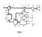
- FIG. 1 shows a block diagram of a circuit arrangement which is supplied with an image signal via a first input 1 of a logic stage 2.
- the image signal becomes an image signal input 4 of a controllable one Amplifier 5 fed, which outputs an output 6 a current controlled by the image signal.
- This is fed via a measuring stage 7 to a hot cathode 8 in an image display tube 9 and forms therein a beam current of a cathode ray, through which an image determined by the image signal is displayed on a fluorescent screen of the image display tube 9.
- the measuring stage 7 measures the current supplied to the hot cathode 8, ie the beam current in the image display tube 9, and outputs a measuring signal corresponding to the magnitude of this current to a measuring signal output 10.
- This is a M eßsignaleingang 11 of a comparison device 12 is supplied, of a reference signal is supplied to a reference signal input. 13
- the comparison arrangement 12 forms a control signal from the value of the measurement signal supplied at the time at the measurement signal input 11 on the one hand and the reference signal on the other by forming a difference and emits it at a control signal output 14. From there, the control signal is fed to an input 15 of a control signal memory 16 and stored therein. Via an output 17 of the control signal memory 16, the control signal is fed to a second input 18 of the logic stage 2, in which it is combined with the image signal, for example added to it.
- the combination stage 2, the controllable amplifier 5, the measuring stage 7, the comparison arrangement 12 and the control signal memory 16 form a control loop with which the beam current is tracked in the sampling interval when the reference level occurs in the image signal of the reference signal.
- a black level or a level with a small, fixed distance from the serves as the reference level Black level, ie a value in the image signal that causes a black or almost black image area in the image display tube in the image shown.
- the described control loop forms a blocking point control for the picture display tube. If the reference level is at a distance from the black level, the control loop is also referred to as quasi blocking point control.
- the circuit arrangement according to FIG. 1 furthermore has a trigger circuit 19, to which the measuring signal from measuring signal output 10 of measuring stage 7 is fed to a measuring signal input 20.
- the trigger circuit 19 is set to a first state in which it blocks the comparison arrangement 12 via a first switching connection 21 in such a way that it does not emit a control signal or a control signal with the value zero at its control signal output 14. This prevents the control signal memory 16 from storing undefined values for the control signal at the moment of start-up or immediately thereafter.
- the circuit arrangement according to FIG. 1 furthermore has a logic network 22 which is connected to the trigger circuit 19 via a second switching connection 23, via which a changeover signal is supplied, and to the controllable amplifier 5 via a third switching connection 24.
- the logic network 22 when the circuit arrangement is started up, is controlled by the changeover signal in a first state in which it blocks the controllable amplifier 5 with a blocking signal via the third switching connection 24 in such a way that none in the picture display tube 9 yet the image signal controlled beam currents can flow. With this, the picture display tube 9 darkened, no picture is shown yet.
- the hot cathode 8 When the image display tube 9 is started up, the hot cathode 8 is still cold, so that no beam current can flow anyway. The hot cathode 8 is now heated up and after a certain time begins to gradually emit electrons, as a result of which a cathode beam and thus a beam current can slowly form. However, this would be indefinite during the heating up of the hot cathode 8, and also because the blocking point control has not yet settled, and is therefore suppressed by the controllable amplifier 5.
- the controllable amplifier 5 outputs 6 at its output 6 only in time intervals which are provided immediately after the cathode rays return to an initial position in the transition from the display of an image to the display of a subsequent image, but before the start of the display of the subsequent image a voltage in the form of an auxiliary pulse briefly, by means of which a beam current is generated in the image display tube 9 if the hot cathode 8 is sufficiently heated.
- the time interval for the delivery of this voltage is selected such that a cathode beam generated by it does not produce a visible image in the image display tube 9 and corresponds, for example, to the sampling interval.
- the measuring stage 7 measures the short-term cathode current generated in the manner described and outputs a corresponding measuring signal at its measuring signal output 10, which is fed to the trigger circuit 19 via the measuring signal input 20. If the measurement signal exceeds a specific, predeterminable threshold value, the trigger circuit 19 is switched to a second state in which it releases the comparison arrangement 12 via the first switching connection 21 and with the second switching connection 23 Switching signal also transferred the logical network 22 into a second state.
- the comparison arrangement 12 now evaluates the her about the M eßsignaleingang from 11 supplied measurement signal, ie it forms the control signal as the difference between the measurement signal and the reference signal supplied via the input 13 a reference signal.
- the control signal is stored in the control signal memory 16 via the control signal output 14 and the input 15.
- the controllable amplifier 5 is switched in the second state of the logic network 22 via the third switching connection 24 by the blocking signals in such a way that the image signal controls the beam currents only during the sampling intervals and that no image otherwise appears in the image display tube.
- the blocking point control begins to settle, i.e. through the control loop formed from logic stage 2, controllable amplifier 5, measuring stage 7, comparison arrangement 12 and control signal memory 16, the value of the control signal is changed until the beam current in the picture display tube 9 at the blocking point or at a fixed point spaced level is adjusted to a value predetermined by the reference signal.
- the sampling interval in which the image signal controls the beam current via the controllable amplifier 5 is selected such that the image signal in it just assumes a value corresponding to the blocking point or the level which is at a fixed distance therefrom.
- the control signal supplied to the control signal memory 16 changes continuously.
- a change detection arrangement 25 which detects the changes in the control signal, is inserted between the control signal output 14 of the comparison arrangement 12 and the input 15 of the control signal memory 16.
- the change detection arrangement 25 emits a change signal at an output 26, which indicates that the steady state of the blocking point control has been reached and is fed to a change signal input 27 of the logic network 22.
- the logic network 22 then switches to a third state in which it releases the controllable amplifier 5 via the third switching connection 24 in such a way that the beam currents are now controlled without restriction by the image signal. A correctly displayed image thus appears in the image display tube 9.
- a shadow-like representation of individual components of the circuit arrangement in FIG. 1 indicates a modification by which this circuit arrangement is set up for displaying color images in the image display tube 9.
- Three color signals for example, are then supplied as the image signal via input 1 of logic stage 2.
- input 1 is drawn in triplicate, and logic stage 2 has a logic element for each of these color signals, e.g. an adder.
- the controllable amplifier 5 now comprises three amplifier stages, one for each of the color signals, the image display tube 9 now contains three hot cathodes 8 instead of one, so that three mutually independent cathode beams are present for the three color signals.
- the comparison arrangement 12 forms partial control signals which are associated with the individual color signals and arrive at the individual beam currents with the reference signal and forwards them to three memory units which are included in the control signal memory 16. From there, the partial control signals reach the assigned logic elements via the second input 18 of logic level 2.
- the circuit arrangement thus forms three independent control loops for blocking point control of the individual color signals, these control loops only having the measuring stage 7 and at least partially the comparison arrangement 12 in common.
- the change detection arrangement 25 now comprises three change detectors, each of which detects the changes over time of the partial control signals belonging to a color signal. Each of these change detectors then outputs a partial change signal to the change signal input 27 of the logic network 22 via the output 26. These partial change signals occur independently of one another when the associated control loop has settled.
- the logic network 22 evaluates all three partial change signals and only switches to its third state when all partial change signals indicate a steady state of the control loops. Only then is it ensured that all color signals from the beam currents controlled by them are correctly reproduced in the image display tube and thus no falsifications of the displayed image, in particular no color falsifications, occur.
- the color image shown then has after its appearance Commissioning of the picture tube immediately its correct brightness and color.
- FIG. 2 shows a somewhat more detailed block diagram of an exemplary embodiment of a circuit arrangement set up for processing an image signal comprising three color signals.
- Three color signals for displaying the colors red, green and blue are supplied to it via three input connections 101, 102, 103.
- a red color signal reaches a first adder 201 via the first input connection 101
- a green color signal reaches a second adder 202 via the second input connection 102
- a blue color signal reaches a third adder 203 via the third input connection 103
- the outputs 301, 302 and 303 of the adders 201, 202, 203 are supplied with the color signals amplifier stages 501, 502 and 503.
- Each of the amplifier stages comprises a switchable amplifier 511, 512 or 513, a power amplifier 521, 522 or 523 and a measuring transistor 531, 532 or 533.
- the emitters of these measuring transistors 531, 532, 533 are each equipped with a hot cathode 801, 802, 803 of the picture display tube 9 and supply the cathode currents, whereas the collectors of the measuring transistors 531, 532, 533 are connected to one another and to a first connection 701 of a measuring resistor 702, the second connection 703 of which is connected to ground.
- the current gain of the measuring transistors 531, 532 and 533 is so great that their collector currents almost match the cathode currents. By measuring the voltage drop generated by the cathode currents at the measuring resistor 702, the cathode currents and thus the beam currents in the image display tube 9 can then be measured with great accuracy.
- the voltage drop across the measuring resistor 702 is fed as a measuring signal to an input 121 of an isolating amplifier 120 with an amplification factor of one, at whose output 122 the unchanged measuring signal is therefore available with low resistance. From there it is fed to a first connection 131 of a reference voltage source 130, which is connected with its second connection 132 to inverting inputs 111, 112 and 113 of three differential amplifiers 123, 124, 125.
- the differential amplifiers 123, 124, 125 also each have a non-inverting input 114, 115 and 116, respectively.
- the input 121 of the isolation amplifier 120 can be connected to ground via a short-circuit switch 127.
- partial control signals belonging to the individual color signals are generated in the form of electrical voltages (or possibly recharge currents) via control signal sampling switches 154, 155 and 156 on the one hand first connections 151, 152 and 153 supplied by control signal storage capacitors 161, 162, 163, which form the storage units of the control signal memory 16, and in which charges corresponding to these voltages (or formed by the charge-reversal currents) are stored.
- the partial control signals are supplied to second inputs 181, 182 and 183 of the first, second and third adders 201, 202 and 203, respectively, and are additively linked therein with the color signals from the first, second and third input connections 101, 102 and 103, respectively .
- 3a shows a horizontal blanking signal for a television signal which controls the beam currents in the image display tube 9 as an image signal. It denotes H horizontal blanking pulses, which follow one another at a time interval in the image signal and by means of which the beam currents are switched off during the line return between the display of individual image lines in the image display tube.
- 3b shows a vertical blanking pulse V, by means of which the beam currents are switched off during the transition from the representation of an image to the representation of the subsequent image.
- 3c shows a measurement signal control pulse VH which is formed from a vertical blanking pulse V extended by three line periods.
- the short-circuit switch 127 is now controlled in such a way that it is only non-conductive for the duration of the measurement signal control pulse VH and short-circuits the input 121 of the isolating amplifier 120 to ground for the rest of the time. As a result, a measurement signal only reaches the comparison arrangement 12 during the image change, so that the parts of the image signal which control the beam currents which generate the image in the image display tube have no influence on the comparison arrangement 12 and thus on the blocking point control.
- the differential amplifier 123, 124, 125 is then at the inverting inputs 111, 112, 113r that one output from the reference voltage source 130 between its first connection 131 and its second connection 132 Reference voltage reduced measurement signal from the output 122. If the differential amplifiers 123, 124, 125 were not present, this difference would be fed directly to the control signal storage capacitors 161, 162, 163 as partial control signals. The differential amplifiers 123, 124, 125 amplify the difference and thus form the control amplifiers of the control loops.
- the comparison arrangement 12 also contains a device for compensating for the influence of any leakage currents that may occur in the image display tube 9.
- the non-inverting inputs 114, 115, 116 of the three differential amplifiers 123, 124 and 125 are supplied with a voltage to which the leakage current storage capacitor 126 is charged .
- This charging takes place through the measurement signal from the output 122 of the isolating amplifier 120 via the decoupling resistor 118 and the leakage current sensing switch 119, which is closed only within the duration of the vertical blanking pulse V, possibly only during part of the same.
- the beam currents are completely switched off by the image signal, so that possibly only a leakage current flows through the measuring resistor 702.
- the measurement signal thus corresponds to this leakage current for the duration of the vertical blanking pulse V. Since the leakage current also flows during the rest of the time, the measurement signal also contains a portion originating from the leakage current outside the period of the vertical blanking pulse V, which portion is therefore also contained in the voltage supplied to the inverting inputs 111, 112, 113 of the differential amplifiers 123, 124, 125 and subtracted out in the differential amplifiers 123, 124, 125.
- the partial control signal from the output 141 of the difference ver amplifier 123 is fed to the third control signal storage capacitor 163 during the period of a storage pulse L2 and the partial control signal from the output 142 of the differential amplifier 124 to the second control signal storage capacitor 162 during a storage pulse L3.
- the memory pulses L1, L2 and L3 are shown in Fig. 3d, e and f. They lie each. one after the other in one of the three line periods by which the measurement signal control pulse VH is longer than the vertical blanking pulse V.
- the switchable amplifiers 511, 512 and 513 each receive a blanking signal BL1, BL2, BL3 at a blanking input 241, 242, 243, the courses of which are shown in FIGS. 3g, h, i. These blanking signals interrupt the supply of the color signals during the line rewinds and the image changes, ie during the period of the measurement signal control pulse VH, and thus the beam currents switched off in these time intervals.
- the red color signal during the first line duration after the end of the vertical blanking pulse V, the blue color signal during the second line duration after the end of the vertical blanking pulse V and the green color signal during the third line duration after the end of the vertical blanking pulse V from the switchable amplifiers 511 , 512, 513 so that they can control the beam currents.
- the blanking signals BL1, BL2 and BL3 interruptions in the frame change blanking pulse, which corresponds to the measurement signal control pulse VH, are provided in the corresponding time intervals.
- the beam currents are measured in these time intervals and partial control signals are determined from the partial measurement signals and are stored in the control signal storage capacitors 161, 162, 163.
- the circuit arrangement according to FIG. 2 also contains a trigger circuit 19, to which a supply voltage is supplied via a supply connection 190. Via a reset input 191, the trigger circuit 19 is also supplied with a voltage from a third connection 133 of the reference voltage source 130. When the circuit arrangement is started up, this voltage is built up with a delay compared to the supply voltage, so that a switch-on / reset signal is generated by the interaction of the two voltages when the circuit arrangement is started up in such a way that a voltage pulse with a low value occurs at the reset input 191 during start-up, which causes the trigger circuit 19 in its first state.
- An arbitrarily designed other circuit can also be connected to the reset input 191, which generates a switch-on reset signal when the picture tube is put into operation.
- the trigger circuit 19 is also connected via a second switching connection 23 to a logic network 22, which is also set to a first state when the circuit arrangement is started up via the second switching connection 23.
- the logic network 22 emits a blocking signal at a blocking output 240, which is fed to the three switchable amplifiers 511, 512, 513.
- the supply of the color signals to the final amplifiers 521, 522, 523 is completely interrupted, so that no beam currents can be generated by them. No picture is therefore shown.
- the trigger circuit 19 and the logic network 22 are further supplied via a line 233 with a key-in pulse EL which extends over the three line periods which the measurement signal control pulse VH is longer than the vertical blanking pulse V, i.e. over the sampling interval.
- this push-in pulse EL is emitted via a control output 192 from the trigger circuit 19 and fed to a pulse generator 244.
- This generates a voltage pulse of a certain magnitude during the duration of the key-in pulse EL and passes it on via switching diodes 245, 246, 247 as an auxiliary pulse to the final amplifiers 521, 522, 523.
- the beam currents are briefly switched on in order to receive a measurement signal despite the color signals being switched off as soon as at least one of the hot cathodes 801, 802, 803 supplies a beam current.
- the trigger circuit 19 In its first state, the trigger circuit 19 also emits a signal via a control line 211, by means of which the outputs 141, 142, 143 of the differential amplifiers 123, 124, 125 are switched to ground potential or almost to ground potential. This turns it into effects of voltages at the inputs 111 to 116 of the differential amplifiers 123, 124, 125, in particular effects of the reference voltage source 130, by which incorrect charging of the control signal storage capacitors 161, 162, 163 can be triggered, are suppressed.
- the measurement signal generated with the aid of the pulse generator 244 at the input 121 of the isolation amplifier 120 is also fed to the trigger circuit 19 via a measurement signal input 20. If it exceeds a predetermined threshold value, the trigger circuit 19 switches to its second state. The logic network 22 is then also switched to its second state via the second switching connection 23.
- the differential amplifiers 123, 124, 125 are also enabled by the signal via the control line 211 to output a control signal determined by the difference in the voltages at their inputs 111 to 116.
- the pulse generator 244 is blocked via the control output 192.
- the blocking signal emitted by the blocking output 240 of the logic network 22 now switches on the switchable amplifiers 511, 512, 513 in the time intervals determined by the storage pulses L1, L2, L3 in such a way that the color signals can cause beam currents in these time intervals to form a measuring signal that the control loops settle. However, the display of the image is still suppressed.
- the control signal storage capacitors 161, 162, 163 are charged.
- Change detectors 251, 252, 253 are arranged in the leads to their first connections 151, 152, 153, which detect the changes in the charging currents of the control signal storage capacitors 161, 162, 163 and which each have a partial output at their outputs 261, 262, 263. Issue change signal when the charging current of the control signal storage probe concerned sator decayed and the associated control loop has settled.
- the partial change signals are fed to three connections 271, 272, 273 of the change signal input 27 of the logic network 22.
- the logic network 22 switches from its second to its third state.
- the blocking signal from the blocking output 240 is now completely switched off in such a way that the switchable amplifiers 511, 512, 513 are only switched by the blanking signals BL1, BL2, BL3.
- the color signals are then switched through to the final amplifiers 521, 522, 523 and the image is displayed in the display tube.
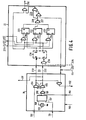
- FIG. 4 shows an exemplary embodiment of a trigger circuit 19 and a logic network 22 of the circuit arrangements according to FIG. 1 or 2.
- the trigger circuit 19 contains a flip-flop formed from two NAND gates 194, 195, which uses the reset input 191 to switch on the reset signal is supplied, by which the trigger circuit 19 is reset to its first state. All elements of the circuit arrangement in Fig. 4 are shown in positive logic.
- the flip-flop 194, 195 is set by a brief low voltage at the reset input 191 immediately after the circuit arrangement has been put into operation such that a high voltage occurs at the output of the first NAND gate 194 and a low voltage occurs at the output of the second NAND gate 195. Due to the low voltage at the output of the second NAND gate 195, the differential amplifiers 123, 124, 125 are blocked via the control line 211 in the manner described.
- the trigger circuit 19 is supplied with the key-in pulse EL via the line 233, linked with the signal from the output of the first NAND gate 194 via an AND gate 196 and output at the control output 192 for controlling the pulse generator 244.
- the signals from the outputs of the NAND gates 194, 195 are fed to the logic network 22 as a switchover signal via a first line 231 and a second line 232 of the second switching connection 23.
- the first line 231 is connected to reset inputs R three of partial change signal memories 221, 222, 223 designed as bistable flip-flops, which are reset when the circuit arrangement is started up via the first line 231 in such a way that they carry a low voltage at their outputs Q.
- the second line 232 of the second switching connection 23 is led via three AND gates 224, 225, 226 to set inputs S of the three partial change signal memories 221, 222, 223.
- the signal on the second line 232 of the second switching connection 23 is linked to one of the partial change signals supplied via the connections 271, 272, 273.
- the signals from the outputs Q of the partial change signal memories 221, 222, 223 are linked via a collecting gate 227 designed as a NAND gate and are provided at its output 228.
- the trigger circuit 19 is supplied with the measurement signal via the measurement signal input 20 and is fed to a first input 197 of a threshold value detector 198, to which a threshold value generated by a threshold value generator 199, for example as a threshold voltage, is also fed at a second input. If the voltage at the first input 197 of the threshold detector 198 is less than the voltage output by the threshold generator 199, the threshold detector 198 outputs a high voltage at its output 200. In contrast, if the voltage at the first input 197 exceeds the voltage of the threshold value generator 199, the voltage at the output 200 jumps to a low value. This voltage is supplied as a set signal to the flip-flop 194, 195, switches it over and thereby sets the trigger circuit 19 into its second state when the voltage at the first input 197 exceeds the voltage of the threshold value generator 199.
- an interrogation gate 181 designed as an OR gate is inserted between the output 200 and the flip-flop 194, 195, to which an interrogation pulse is fed to the trigger circuit 19 via an interrogation input 193.
- a pulse which occurs in the second line period after the end of the vertical blanking pulse V e.g. corresponds essentially to the storage pulse L2.
- a further flip-flop 234 is inserted into the lines 231, 232 to delay the signals passed through them, which is reset when the circuit arrangement is started up via the first line 231 and thus also resets the partial change signal memories 221, 222, 223.
- the further flip-flop 234 is only set via the second line 232 of the second switching connection 23 when an enable pulse arrives via an enable input 235 and a further AND gate 236, for example by a period of approximately the distance between two vertical blanking pulses V after switching the trigger circuit 19 into the second state. With this e.g. a period can be bridged in which no defined signal values are present at the connections 271, 272, 273.
- the signal at the output 228 of the collective gate 227 changes its state when the last of the three partial change signals has also arrived and has set the last of the three partial change signal memories. It is then via a gate arrangement 229 comprising two NAND gates and an AND gate with the key-in pulse EL from line 233 and the signal on the second line 232 of the second switching connection 23 or from the output Q of the further trigger circuit 234 to that at the blocking output 240 emitted blocking signal linked, which is fed to the switchable amplifiers 511, 512, 513.
- m, n show the combinations of the blocking signal with the blanking signals BL1, BL2 and BL3 at the blanking inputs 241, 242, 243 of the switchable amplifiers 511, 512, 513 in the manner of logical AND operations.
- the dash-dotted lines show resulting key-in signals A1 formed by these links, A2, A3 after start-up of the circuit arrangement and before the occurrence of a beam current, in other words in the first state of the logic network 22.
- the resulting key-in signals A1, A2, A3 are constantly at a low level.
- the dashed curves show the resulting key-in signals A1, A2, A3 after the occurrence of a beam current and before reaching the steady state of the blocking point control, ie in the second state of the logic network 22, while the solid curves show the resultant key-in signals A1, A2, A3 in the steady state of Represent blocking point control, ie in the third state of the logical network 22.
- the curves drawn in dashed lines correspond in their courses to the storage pulses L1, L2, L3, while the solid curves in their courses correspond to the inverses of the blanking signals BL1, BL2, BL3.
- a high level of the resulting key-in signal A1, A2 or A3 means that the switchable amplifier 511, 512 or 513 supplies the color signal to the associated power amplifier 521, 522 or 523, while a low level in the resultant key-in signal A1, A2 or A3 A3 means that the associated switchable amplifier 511, 512 or 513 is blocked for the color signal.
- the circuit arrangement described is designed in such a way that the trigger circuit 19 remains in its second state and the logic network 22 in its third state, even if charging currents occur again at the differential signal storage capacitors 161, 162, 163 due to faults during the operation of the circuit arrangement.
- the blocking point control then adjusts without disturbing the displayed image.
- the green color signal can also be used during the second line duration after the end of the vertical blanking pulse V and the blue color signal during the third line period after the end of the vertical blanking pulse V by the switchable amplifiers 511, 512, 513 to control the beam currents.
- the memory pulses L2 and L3 are then exchanged at the control signal sampling switches 155 and 156 and the second and third blanking signals BL2 and BL3 at the blanking inputs 242 and 243.
- the resulting key-in signals A2 and A3 according to FIGS. 3m and n are then exchanged.
- a broken line 900 indicates which components of the circuit arrangement can advantageously be combined to form an integrated circuit.
- the first connections 151, 152, 153 of the differential signal storage capacitors 161, 162, 163, a connection 128 of the leakage current storage capacitor 126, three connections 524, 525, 526 in the feed lines to the power amplifiers 521, 522, 523 and a line connection 704 between the first connection 701 of the measuring resistor 702 and the input 121 of the isolating amplifier 120 are then formed as connection contacts of this integrated circuit.
Landscapes
- Engineering & Computer Science (AREA)
- Multimedia (AREA)
- Signal Processing (AREA)
- Processing Of Color Television Signals (AREA)
- Testing, Inspecting, Measuring Of Stereoscopic Televisions And Televisions (AREA)
- Television Receiver Circuits (AREA)
- Video Image Reproduction Devices For Color Tv Systems (AREA)
Applications Claiming Priority (2)
| Application Number | Priority Date | Filing Date | Title |
|---|---|---|---|
| DE19843437952 DE3437952A1 (de) | 1984-10-17 | 1984-10-17 | Schaltungsanordnung zum steuern einer bildwidergaberoehre |
| DE3437952 | 1984-10-17 |
Publications (3)
| Publication Number | Publication Date |
|---|---|
| EP0178734A2 true EP0178734A2 (fr) | 1986-04-23 |
| EP0178734A3 EP0178734A3 (en) | 1987-05-20 |
| EP0178734B1 EP0178734B1 (fr) | 1988-12-28 |
Family
ID=6248042
Family Applications (1)
| Application Number | Title | Priority Date | Filing Date |
|---|---|---|---|
| EP85201665A Expired EP0178734B1 (fr) | 1984-10-17 | 1985-10-11 | Circuit de commande d'une tube de reproduction d'image |
Country Status (6)
| Country | Link |
|---|---|
| US (1) | US4698557A (fr) |
| EP (1) | EP0178734B1 (fr) |
| JP (1) | JPS6198089A (fr) |
| CN (1) | CN1006590B (fr) |
| DE (2) | DE3437952A1 (fr) |
| FI (1) | FI78590C (fr) |
Cited By (2)
| Publication number | Priority date | Publication date | Assignee | Title |
|---|---|---|---|---|
| EP0239014A3 (fr) * | 1986-03-26 | 1990-02-21 | Blaupunkt-Werke GmbH | Méthode et dispositifs de régulation du point de fonctionnement d'étages finaux vidéo |
| EP0542347A3 (en) * | 1991-11-13 | 1995-04-12 | Philips Nv | Display device including a black level setting circuit |
Families Citing this family (9)
| Publication number | Priority date | Publication date | Assignee | Title |
|---|---|---|---|---|
| US4660093A (en) * | 1986-05-09 | 1987-04-21 | Rca Corporation | Television receiver with delayed display |
| US5025196A (en) * | 1986-06-02 | 1991-06-18 | Canon Kabushiki Kaisha | Image forming device with beam current control |
| US5148088A (en) * | 1991-10-01 | 1992-09-15 | North American Philips Corporation | Limiting X-ray production in an operating CRT |
| JP3254717B2 (ja) * | 1992-02-18 | 2002-02-12 | ソニー株式会社 | 映像表示装置 |
| CA2145901C (fr) * | 1994-04-28 | 2000-02-22 | Anton Werner Keller | Dispositif d'attaque a correction du gamma pour kinescope |
| US6226037B1 (en) * | 1998-07-28 | 2001-05-01 | Thomson Licensing S.A. | AKB interface circuit for kine driver IC |
| US6894445B2 (en) * | 2001-08-31 | 2005-05-17 | Thomson Licensing S.A. | Cathode ray tube phosphor protection |
| US12443259B2 (en) * | 2022-11-23 | 2025-10-14 | Cisco Technology, Inc. | Remote switch synchronization for pulse power and fault managed power (FMP) applications |
| CN117590838B (zh) * | 2024-01-19 | 2024-05-03 | 深圳市凯威达电子有限公司 | 一种微处理器老化智能检测方法及系统 |
Family Cites Families (4)
| Publication number | Priority date | Publication date | Assignee | Title |
|---|---|---|---|---|
| GB1575604A (en) * | 1976-01-27 | 1980-09-24 | Bang & Olufsen As | Colour television receivers |
| US4263622A (en) * | 1979-01-30 | 1981-04-21 | Rca Corporation | Automatic kinescope biasing system |
| FR2461418A1 (fr) * | 1979-07-09 | 1981-01-30 | Videocolor | Procede d'elaboration et de correction automatiques de la tension de blocage d'un canon a electrons et dispositif pour la mise en oeuvre de ce procede |
| DE3218505C1 (de) * | 1982-05-17 | 1983-11-24 | Siemens AG, 1000 Berlin und 8000 München | Fernseheinrichtung mit einer Schaltungsanordnung zur Kompensation von Amplitudenaenderungen |
-
1984
- 1984-10-17 DE DE19843437952 patent/DE3437952A1/de not_active Withdrawn
-
1985
- 1985-10-11 EP EP85201665A patent/EP0178734B1/fr not_active Expired
- 1985-10-11 DE DE8585201665T patent/DE3567139D1/de not_active Expired
- 1985-10-14 FI FI853975A patent/FI78590C/fi not_active IP Right Cessation
- 1985-10-14 CN CN85107568A patent/CN1006590B/zh not_active Expired
- 1985-10-15 US US06/787,395 patent/US4698557A/en not_active Expired - Lifetime
- 1985-10-17 JP JP60230034A patent/JPS6198089A/ja active Granted
Cited By (2)
| Publication number | Priority date | Publication date | Assignee | Title |
|---|---|---|---|---|
| EP0239014A3 (fr) * | 1986-03-26 | 1990-02-21 | Blaupunkt-Werke GmbH | Méthode et dispositifs de régulation du point de fonctionnement d'étages finaux vidéo |
| EP0542347A3 (en) * | 1991-11-13 | 1995-04-12 | Philips Nv | Display device including a black level setting circuit |
Also Published As
| Publication number | Publication date |
|---|---|
| EP0178734A3 (en) | 1987-05-20 |
| CN85107568A (zh) | 1986-04-10 |
| CN1006590B (zh) | 1990-01-24 |
| JPH0513431B2 (fr) | 1993-02-22 |
| JPS6198089A (ja) | 1986-05-16 |
| FI78590C (fi) | 1989-08-10 |
| DE3437952A1 (de) | 1986-04-17 |
| FI853975A0 (fi) | 1985-10-14 |
| US4698557A (en) | 1987-10-06 |
| DE3567139D1 (en) | 1989-02-02 |
| EP0178734B1 (fr) | 1988-12-28 |
| FI78590B (fi) | 1989-04-28 |
| FI853975L (fi) | 1986-04-18 |
Similar Documents
| Publication | Publication Date | Title |
|---|---|---|
| DE2808600C2 (fr) | ||
| DE3533922C2 (de) | Festkörper-Bildabtastvorrichtung | |
| DE3842279A1 (de) | Lichtintensitaetsdetektorschaltung | |
| DE3102157C2 (fr) | ||
| DE3014984C2 (de) | Schaltungsanordnung zur automatischen Regelung des Austaststrompegels einer Bildröhre | |
| EP0178734B1 (fr) | Circuit de commande d'une tube de reproduction d'image | |
| DE3419282C2 (de) | Strahlstromregelschaltung | |
| DE2618531C2 (de) | Korrekturschaltungsanordnung für eine Fernsehröhre | |
| DE2737551C3 (de) | Farbfernsehgerät | |
| DE3786830T2 (de) | System zur automatischen Einstellung der Farbtemperatur. | |
| DE2902366A1 (de) | Fernsehbildwiedergabeanordnung | |
| DE2442201C3 (de) | Schaltungsanordnung zum Gebrauch bei einer Fernsehaufnahmeröhre, die mit einem Antikometenschweif-Elektronenstrahlerzeugungssystem versehen ist | |
| DE2622866B2 (de) | Schaltungsanordnung in einem Farbfernsehempfänger zur Änderung des Kontraste bei gleichbleibender Sättigung | |
| DE2616728B2 (de) | Schaltungsanordnung zum Ansteuern der Bildwiedergabeeinrichtung eines Farbfernsehempfängers | |
| DE3425551C2 (de) | Regelschaltung zum Regeln der Weißbalance | |
| DE2403267B2 (de) | Fernsehbildwiedergabeanordnung mit einer Strahlstromklemmregelschaltung | |
| DE69219867T2 (de) | Kontraststrahlstrombegrenzungsanordnung mit sekundären Helligkeitstrahlstrombegrenzungsvorrichtungen | |
| DE1156844B (de) | Saegezahnspannungsgenerator, insbesondere zur zeitlinearen Ablenkung des Abtastflecks von Elektronenstrahlen | |
| DE2704193C3 (fr) | ||
| DE3146926C2 (de) | Farbfernsehempfänger | |
| DE2820243A1 (de) | Farbpegel-regelungsschaltung | |
| DE3339195C2 (fr) | ||
| DE3908271C2 (fr) | ||
| DE3048104A1 (de) | "frequenzdemodulationsanordnung" | |
| DE3339194C2 (fr) |
Legal Events
| Date | Code | Title | Description |
|---|---|---|---|
| PUAI | Public reference made under article 153(3) epc to a published international application that has entered the european phase |
Free format text: ORIGINAL CODE: 0009012 |
|
| AK | Designated contracting states |
Kind code of ref document: A2 Designated state(s): DE FR GB IT |
|
| PUAL | Search report despatched |
Free format text: ORIGINAL CODE: 0009013 |
|
| AK | Designated contracting states |
Kind code of ref document: A3 Designated state(s): DE FR GB IT |
|
| 17P | Request for examination filed |
Effective date: 19870720 |
|
| RAP1 | Party data changed (applicant data changed or rights of an application transferred) |
Owner name: N.V. PHILIPS' GLOEILAMPENFABRIEKEN Owner name: PHILIPS PATENTVERWALTUNG GMBH |
|
| 17Q | First examination report despatched |
Effective date: 19880311 |
|
| GRAA | (expected) grant |
Free format text: ORIGINAL CODE: 0009210 |
|
| AK | Designated contracting states |
Kind code of ref document: B1 Designated state(s): DE FR GB IT |
|
| REF | Corresponds to: |
Ref document number: 3567139 Country of ref document: DE Date of ref document: 19890202 |
|
| ITF | It: translation for a ep patent filed | ||
| GBT | Gb: translation of ep patent filed (gb section 77(6)(a)/1977) | ||
| ET | Fr: translation filed | ||
| PLBE | No opposition filed within time limit |
Free format text: ORIGINAL CODE: 0009261 |
|
| STAA | Information on the status of an ep patent application or granted ep patent |
Free format text: STATUS: NO OPPOSITION FILED WITHIN TIME LIMIT |
|
| 26N | No opposition filed | ||
| PGFP | Annual fee paid to national office [announced via postgrant information from national office to epo] |
Ref country code: FR Payment date: 19911023 Year of fee payment: 7 |
|
| ITTA | It: last paid annual fee | ||
| PG25 | Lapsed in a contracting state [announced via postgrant information from national office to epo] |
Ref country code: FR Effective date: 19930630 |
|
| REG | Reference to a national code |
Ref country code: FR Ref legal event code: ST |
|
| PGFP | Annual fee paid to national office [announced via postgrant information from national office to epo] |
Ref country code: GB Payment date: 19991021 Year of fee payment: 15 |
|
| PGFP | Annual fee paid to national office [announced via postgrant information from national office to epo] |
Ref country code: DE Payment date: 19991215 Year of fee payment: 15 |
|
| PG25 | Lapsed in a contracting state [announced via postgrant information from national office to epo] |
Ref country code: GB Free format text: LAPSE BECAUSE OF NON-PAYMENT OF DUE FEES Effective date: 20001011 |
|
| GBPC | Gb: european patent ceased through non-payment of renewal fee |
Effective date: 20001011 |
|
| PG25 | Lapsed in a contracting state [announced via postgrant information from national office to epo] |
Ref country code: DE Free format text: LAPSE BECAUSE OF NON-PAYMENT OF DUE FEES Effective date: 20010703 |