EP0178954B1 - Verfahren und Einrichtung zur Abtastung eines Fensters im Bildbereich einer bildorganisierten Ladungsübertragungsanordnung - Google Patents
Verfahren und Einrichtung zur Abtastung eines Fensters im Bildbereich einer bildorganisierten Ladungsübertragungsanordnung Download PDFInfo
- Publication number
- EP0178954B1 EP0178954B1 EP85401098A EP85401098A EP0178954B1 EP 0178954 B1 EP0178954 B1 EP 0178954B1 EP 85401098 A EP85401098 A EP 85401098A EP 85401098 A EP85401098 A EP 85401098A EP 0178954 B1 EP0178954 B1 EP 0178954B1
- Authority
- EP
- European Patent Office
- Prior art keywords
- line
- image
- shifting means
- zone
- lines
- Prior art date
- Legal status (The legal status is an assumption and is not a legal conclusion. Google has not performed a legal analysis and makes no representation as to the accuracy of the status listed.)
- Expired - Lifetime
Links
Images
Classifications
-
- H—ELECTRICITY
- H04—ELECTRIC COMMUNICATION TECHNIQUE
- H04N—PICTORIAL COMMUNICATION, e.g. TELEVISION
- H04N25/00—Circuitry of solid-state image sensors [SSIS]; Control thereof
- H04N25/40—Extracting pixel data from image sensors by controlling scanning circuits, e.g. by modifying the number of pixels sampled or to be sampled
- H04N25/44—Extracting pixel data from image sensors by controlling scanning circuits, e.g. by modifying the number of pixels sampled or to be sampled by partially reading an SSIS array
- H04N25/443—Extracting pixel data from image sensors by controlling scanning circuits, e.g. by modifying the number of pixels sampled or to be sampled by partially reading an SSIS array by reading pixels from selected two-dimensional [2D] regions of the array, e.g. for windowing or digital zooming
-
- H—ELECTRICITY
- H04—ELECTRIC COMMUNICATION TECHNIQUE
- H04N—PICTORIAL COMMUNICATION, e.g. TELEVISION
- H04N25/00—Circuitry of solid-state image sensors [SSIS]; Control thereof
- H04N25/70—SSIS architectures; Circuits associated therewith
- H04N25/71—Charge-coupled device [CCD] sensors; Charge-transfer registers specially adapted for CCD sensors
- H04N25/72—Charge-coupled device [CCD] sensors; Charge-transfer registers specially adapted for CCD sensors using frame transfer [FT]
Definitions
- the present invention relates to a method and a device for exploring a window of the image area of a charge transfer device of the frame transfer type.
- an initialization and integration phase (A O ) allows the formation of an image (integration) on the image zone ZI of the charge transfer device, after a possible "cleaning" of the latter. (initialization) by erasing to avoid the effects of persistence.
- phase A1 the image area ZI is entirely copied into the memory area ZM by simultaneous actuation of the first and second aforementioned shifting means; this corresponds to the sending of a comb of 288 pulses on the inputs DI and DM of these respective shifting means.
- phase A2 and A'2 we shift a line from the memory area (single pulse on the DM input) and read the shift register RD (comb of 384 pulses at the DR input third shifting means), which allows the video signal corresponding to this line to be output. This is repeated for the next line, and so on until the memory area is exhausted.
- values corresponding to the European video standard are preferably chosen, namely frame and line durations of 20 ms (50 Hz) and 64 ⁇ s, respectively.
- the duration of steps A1 .... A''2 is at least 18.72 ms.
- a pure delay is created at least equal to 18.72 ms, that is to say of the same order of magnitude as the sampling period (20 ms).
- One of the aims of the invention is to overcome this drawback, by reducing in significant proportions the pure delay inherent in the conventional mode of exploration of charge transfer devices.
- the invention thereby allows the use of these devices in very short response time systems.
- the method of the invention applies each time that one wishes to explore a window of p lines of q pixels, that is to say each time that one is interested only in a determined portion of the image area.
- the invention applies in particular to deviation measurement or video tracking devices, where a processing window centered on a previously designated target has already been defined.
- the position of the window inside the image area and, possibly, its dimensions are determined by calculation (for example a barycenter calculation); they can be variable from one frame to the next according to the movements of the target.
- the integration step is preceded by a step of erasing the image and memory areas, performed by activating the first and second shifting means so as to shift each of the image and memory areas by m lines.
- the start of the erasing step is delayed relative to the end of the window exploration step for the previous frame, this delay being a variable delay, decreasing progressively that the average intensity of the light flux striking the window decreases, so as to adjust to this intensity the duration of the consecutive integration step.
- the third shifting means can be activated, during the same reading of the shift register, at two operating frequencies, namely a slow frequency corresponding to the q useful pixels of the line, and a fast frequency corresponding to the n - q other pixels.
- the fast frequency is for example double the slow frequency.
- the timing circuit also cooperates, in a prior erasure phase preceding the integration step, with the first and second shifting means for shifting each of the image and memory areas by m lines.
- the first and second shifting means for shifting each of the image and memory areas by m lines.
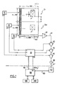
- FIG. 1 there is shown a charge transfer device of the frame transfer type, formed by an image area ZI, a memory area ZM and a shift register RD.
- the shift register RD is formed by a single elementary charge transfer device with 384 positions.
- First shifting means 10 make it possible to move the content of all the elementary charge transfer devices in the image area from one position, towards the memory area ZM. In other words, the content of the image zone ZI is shifted down one line.
- This offset is produced by sending pulses to the input DI of the shifting means 10, a pulse corresponding to an offset of one line (the duration of the offset is generally 1 ⁇ s per line, corresponding to a frequency of recurrence of the 1 MHz pulses).
- second shifting means 20 make it possible to shift the content of the memory zone ZM in the direction of the shift register, by applying pulses to the input DM, with the same clock frequency as for the first means shifters 10.
- third shifting means 30 make it possible to empty the content of the shift register RD to an amplifier 50, thus corresponding to the sequential reading of the line loaded in this register.
- the reading of this is carried out by sending pulses to the DR input, at a clock frequency allowing the reading of a line in 64 ⁇ s.
- the different shifting means are supplied with pulses by a timing circuit 40, the operating sequence of which will be described later.
- the video signal SV is processed by a sample-and-hold stage 60, which smoothes the video signal by eliminating the portions comprised between the different pixels. Then, a clamping stage brings the black reference points delivered by the charge transfer device to each line to zero volt level. The next stage 80 allows a cleaning ("blanking") by leveling zero volts of the video signal during the periods which do not correspond to any image. Finally, a stage 90 performs the impedance and level adaptation, to transmit the video signal SV 'thus processed to the circuits allowing its analysis.
- These analysis circuits include a microprocessor assembly 100 connected by a bi-directional serial link to an analog-digital converter 110 ensuring the real-time digitization of the video signal SV '.
- RAM 130 and ROM 140 are associated with the microprocessor assembly 100, which also communicates with the timing circuit 40 by means of a link 150 and a line for transmitting a synchronization signal SY to a reference frame frequency, generally 50 Hz.
- the link 150 makes it possible to exchange information such as that: elimination of the signal corresponding to defective points of the charge transfer device (the coordinates of which are kept in the RAM 130) by temporary inhibition of the blocking sampler 60; modification of the sequencing to adjust the sensitivity of the device to the average lumination of the scene observed; determination of the coordinates and the dimensions of a processing window F; exchange of synchronization pulses, in particular end of line synchronization.
- the invention applies to the situation in which it is desired to explore a window F of reduced dimensions inside the image area; this window has a dimension of p rows and q columns (for example 128 rows x 128 columns); it is at a position in the image area such that there are x lines separating it from the border between image area and memory area, and y columns separating it from the edge of the image area corresponding to the start of the lines.
- the reference F designates the homologous position of this window in the memory zone ZM.
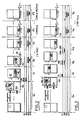
- a first way to explore this window is to use the scanning mode of the prior art, as illustrated in FIG. 2: firstly, after initialization, the photosensitive sites of the image area are excited during an integration phase, so as to transform the lumination into an electric charge. At the end of this integration phase, the image area is copied into the memory area (phase A1), by simultaneous actuation of the first and second shifting means, that is to say by sending a comb of 288 pulses (corresponding to a downward shift of 288 lines in each zone) on each of the DI and DM inputs.
- each line includes (phase A2) sending a pulse to the DM input to shift it down one step the memory area and thus load the shift register with the adjacent line of the memory area, then send a comb of 384 pulses to the DR input, to empty this shift register to the video signal amplifier 50.
- the duration of the phases A1, A2, .... A''2 is at least 18.72 ms, corresponding to a complete exploration of the image area; this value is that of the pure delay which the invention proposes to reduce.
- the exploration mode, according to the invention, of the window F is illustrated in FIG. 3: after initialization and integration (phase B O ), a comb of x pulses is sent to the input DI (the value of x is known by the microprocessor circuit 100 and transmitted to the timing circuit by the bus 150), which has the effect of bringing, in the image area, the window F adjacent to the border between image area and memory area .
- phase B3 a comb of (288 - 128) pulses is sent to the input DM of the second shifting means, which has the effect of bringing, into the memory area, the first line of the window adjacent to the border between memory area and shift register.
- the minimum total duration of the phases B1, B2 ?? B4 is between 8.48 and 8.64 ms. We see that the pure delay has been reduced to the acquisition of more than half of its previously recognized value.
- This period of time can be used to carry out additional "cleaning" scans of the image area, avoiding the afterglow phenomena well known for charge transfer devices.
- the image and memory zones are completely erased by providing for a complete transfer of the image and memory zones, but without any reading of the shift register. This transfer represents a rapid evacuation of the charges accumulated in these two zones.
- an automatic sensitivity adjustment of the device is provided to reduce the duration of the integration phase in the event of excessive lumination.
- the cleaning transfer is given a position that is variable in time, that is to say that this transfer is not necessarily carried out at the start of the frame (this start of the frame being identified by the synchronization signal SY), but it can be delayed by a value that is all the higher as one wishes to reduce the integration time, therefore reducing the sensitivity of the device.
- This adjustment of the time position of the cleaning transfer is determined by the sequencing means 40, under the control of the microprocessor circuit 100 which analyzes the image.
- the frame frequency which corresponds to the periodicity of the refreshment of the information processed by the microprocessor 100, remains unchanged despite the variation in the integration time, and always remains fixed at 20 ms in the example chosen, which always leaves the computer the same time to carry out its processing.
Landscapes
- Engineering & Computer Science (AREA)
- Multimedia (AREA)
- Signal Processing (AREA)
- Transforming Light Signals Into Electric Signals (AREA)
- Facsimile Scanning Arrangements (AREA)
Claims (10)
- Verfahren zum Abtasten eines Fensters (F) mit p Zeilen mit je q Pixeln einer bildorganisierten Ladungsübertragungseinrichtung, wobei diese Ladungsübertragungseinrichtung aufweist:- einen Bildbereich (ZI) in der Fokusebene einer dioptrischen Vorrichtung, der in Matrixform mit m Zeilen mit je n lichtempfindlichen Stellen aufgebaut ist,- einen angrenzenden Blindspeicherbereich (ZM), der in Matrixform mit m Zeilen mit je n Speicherpositionen aufgebaut ist,- ein n-stelliges Schieberegister (RD),
die Abtastschaltkreise dieser Ladungsübertragungseinrichtung aufweisen:- eine erste Verschiebevorrichtung (10) für zeilenweise parallele Ladungsverschiebung in jeder Spalte des Bildbereiches in Richtung auf den Speicherbereich zu,- eine zweite Verschiebevorrichtung (20) für zeilenweise parallele Ladungsverschiebung in jeder Spalte des Bildbereiches in Richtung auf das Schieberegister zu,- eine dritte Verschiebevorrichtung (30) für serielles Lesen des Schieberegisters mit einer gegebenen Sortierfrequenz derart, daß am Ausgang ein Videosignal (SV) ausgegeben wird,
und wobei das Verfahren durch folgende Verfahrensschritte gekennzeichnet ist:- Integration (B0) des auf die lichtempfindlichen Stellen des Bildbereiches fallenden Lichtstromes,- Vor-Verschieben (B1-B3) der (m + x)-zeiligen Bild- und Speicherbereiche, wobei x die Anzahl die die erste Fensterzeile von der Grenze zwischen dem Bildbereich und dem Speicherbereich trennenden Zeilen ist, durch Mitführen dieser ersten an die Grenze zwischen dem Speicherbereich und dem Schieberegister angrenzenden Fensterzeile,- sequentielles Abtasten des Fensters durch, p-mal, wiederholtes Ausführen der folgenden Schritte (B4) mit einer gegebenen Zeilenfrequenz:- Inbetriebsetzen der zweiten Verschiebevorrichtung zum Verschieben des Speicherbereiches um eine Zeile,- Inbetriebsetzen der dritten Verschiebevorrichtung zum seriellen Lesen des Schieberegisterinhaltes. - Verfahren nach Anspruch 1, dadurch gekennzeichnet, daß die Vor-Verschiebungsschritte die folgenden Verfahrensschritte umfassen:- Inbetriebsetzen der ersten Verschiebevorrichtung (B1) derart, daß der Bildbereich um eine Anzahl von Teilen gleich der Anzahl x, der die ersten Fensterzeile von der Grenze zwischen dem Bildbereich und dem Speicherbereich trennenden Linien, verschoben wird,- gleichzeitiges Inbetriebsetzen der ersten und zweiten Verschiebevorrichtung (B2) derart, daß der gesamte Bildbereich und der gesamte Speicherbereich um p Zeilen verschoben wird,- Inbetriebsetzen der zweiten Verschiebevorrichtung (B3) derart, daß der Speicherbereich um (m - p) Zeilen verschoben wird.
- Verfahren nach Anspruch 1 oder 2, dadurch gekennzeichnet, daß dem Integrationsschritt das Löschen des Bildbereiches und des Speicherbereiches vorangeht, das durch Inbetriebsetzen der ersten und der zweiten Verschiebevorrichtung derart, daß sie sowohl den Bildbereich als auch den Speicherbereich um m Zeilen verschieben, ausgeführt wird.
- Verfahren nach Anspruch 3, dadurch gekennzeichnet, daß der Beginn des Löschvorgangs abhängig vom Ende der Fensterabtastung des vorhergehenden Bildes verzögert ist, wobei diese Verzögerung einstellbar, mit der mittleren Intensität des auf das Fenster fallenden Lichtstromes zunehmend ist derart, daß die Dauer des nachfolgenden Integrationsschrittes an diese Intensität angepaßt wird.
- Verfahren nach einem der Ansprüche 1 bis 3, dadurch gekennzeichnet, daß die dritte Verschiebevorrichtung während ein und desselben Lesens des Schieberegisters mit zwei Betriebsfrequenzen in Betrieb gesetzt werden kann, nämlich einer langsamen Frequenz entsprechend der q Nutzpixel der Zeile und einer schnellen Frequenz entsprechend der (n - q) anderen Pixel.
- Verfahren nach Anspruch 5, dadurch gekennzeichnet, daß die schnelle Frequenz das Doppelte der langsamen Frequenz beträgt.
- Abtastschaltkreis zum Inbetriebsetzen des Verfahrens nach einem der vorangehenden Ansprüche, der mit einer Einrichtung für die bildorganisierte Ladungsübertragung zusammenwirkt, wobei diese Einrichtung aufweist:- einen Bildbereich (ZI) in der Fokusebene einer dioptrischen Vorrichtung, der in Matrixform mit m Zeilen mit je n-lichtempfindlichen Stellen aufgebaut ist, welcher die Intensität des einfallenden Lichtstromes im Laufe eines Integrationsschrittes berechnen kann,- einen angrenzenden Blindspeicherbereich (ZM), der in Matrixform mit m Zeilen mit je n Speicherpositionen aufgebaut ist,- ein n-stelliges Schieberegister (RD),
der Abtastschaltkreis aufweist:- eine erste Verschiebevorrichtung (10) für zeilenweise parallele Ladungsverschiebung in jeder Spalte des Bildbereiches in Richtung auf den Speicherbereich zu,- eine zweite Verschiebevorrichtung (20) für zeilenweise parallele Ladungsverschiebung in jeder Spalte des Speicherbereiches in Richtung auf das Schieberegister zu,- eine dritte Verschiebevorrichtung (30) für serielles Lesen des Schieberegisters mit einer gegebenen Sortierfrequenz, derart daß am Ausgang ein Videosignal (SV) ausgegeben wird,
und wobei dieser Schaltkreis dadurch gekennzeichnet ist, daß er darüber hinaus einen Taktgeber (40) aufweist, welcher zusammenwirkt:- mit der ersten und zweiten Verschiebevorrichtung in einer ersten Phase, um eine Vor-Verschiebung des Bildbereiches und des Speicherbereiches um eine vorgegebene Anzahl von Linien zu bewirken,- mit der zweiten und dritten Verschiebevorrichtung in einer zweiten Phase derart, daß ein an das Schieberegister angrenzender Bereich des Speicherbereiches zeilenweise sequentiell abgetastet wird, wobei dieser Bereich einem Nutz-Fenster (F) mit verringerten Abmessungen entspricht, welches ursprünglich im Innern des Bildbereichs enthalten war. - Abtastschaltkreis nach Anspruch 7, dadurch gekennzeichnet, daß der Taktgeber auch in einer dem Integrationsschritt vorgeschalteten Vor-Löschphase mit der ersten und zweiten Verschiebevorrichtung zusammenwirkt, um eine Verschiebung sowohl des Bildbereiches als auch des Speicherbereiches um m Zeilen zu bewirken.
- Abtastschaltkreis nach Anspruch 8, dadurch gekennzeichnet, daß weiterhin eine Vorrichtung zum Anpassen der Empfindlichkeit der Einrichtung vorgesehen ist, die den Beginn der Löschphase gegenüber dem Ende der Fensterabtastphase um eine variablen Zeitabschnitt verzögern kann, welcher mit der mittleren Intensität des in das Fenster einfallenden Lichtstromes wächst, so daß die Dauer des Integrationsschrittes an diese Intensität angepaßt wird.
- Abtastschaltkreis nach einem der Ansprüche 7 bis 9, dadurch gekennzeichnet, daß die dritte Verschiebevorrichtung während ein und desselben Lesens des Schieberegisters mit zwei Betriebsfrequenzen in Betrieb gesetzt werden kann, nämlich einer langsamen Frequenz entsprechend der q Nutzpixel der Zeile und einer schnellen Frequenz entsprechend der (n - q) anderen Pixel.
Applications Claiming Priority (2)
| Application Number | Priority Date | Filing Date | Title |
|---|---|---|---|
| FR8409390 | 1984-06-15 | ||
| FR8409390A FR2566219B1 (fr) | 1984-06-15 | 1984-06-15 | Procede et dispositif pour l'exploration d'une fenetre de la zone image d'un dispositif a transfert de charges du type a transfert de trames |
Publications (3)
| Publication Number | Publication Date |
|---|---|
| EP0178954A2 EP0178954A2 (de) | 1986-04-23 |
| EP0178954A3 EP0178954A3 (en) | 1988-07-13 |
| EP0178954B1 true EP0178954B1 (de) | 1991-10-09 |
Family
ID=9305060
Family Applications (1)
| Application Number | Title | Priority Date | Filing Date |
|---|---|---|---|
| EP85401098A Expired - Lifetime EP0178954B1 (de) | 1984-06-15 | 1985-06-04 | Verfahren und Einrichtung zur Abtastung eines Fensters im Bildbereich einer bildorganisierten Ladungsübertragungsanordnung |
Country Status (5)
| Country | Link |
|---|---|
| US (1) | US4644405A (de) |
| EP (1) | EP0178954B1 (de) |
| DE (1) | DE3584346D1 (de) |
| ES (1) | ES8700825A1 (de) |
| FR (1) | FR2566219B1 (de) |
Families Citing this family (33)
| Publication number | Priority date | Publication date | Assignee | Title |
|---|---|---|---|---|
| US4769710A (en) * | 1985-10-06 | 1988-09-06 | Fuji Photo Film Co., Ltd. | Method for controlling accumulation type photoelectric conversion element |
| FR2593986B1 (fr) * | 1986-01-24 | 1988-04-08 | Thomson Csf | Systeme de lecture rapide d'un capteur optique matriciel a transfert de charges organise en transfert de trame monocoup pour la detection video d'images breves |
| FR2594280B1 (fr) * | 1986-02-07 | 1988-05-27 | Aerospatiale | Senseur opto-electronique a transfert de charges |
| JPS63153971A (ja) * | 1986-07-04 | 1988-06-27 | Hitachi Ltd | 固体撮像装置 |
| EP0251790A3 (de) * | 1986-07-04 | 1989-11-23 | Hitachi, Ltd. | Festkörperbildaufnahme-Vorrichtung |
| DE3628147C1 (de) * | 1986-08-19 | 1988-01-07 | Kappa Messtechnik Gmbh | Verfahren zum Aufnehmen und Speichern von Bildern in schneller Folge |
| FR2604320B1 (fr) * | 1986-09-19 | 1988-11-04 | Thomson Csf | Systeme de prise de vues en videographie rapide utilisant un capteur optique matriciel a transfert de charges |
| US4722007A (en) * | 1986-12-02 | 1988-01-26 | Rca Corporation | TV receiver having zoom processing apparatus |
| EP0282993B1 (de) * | 1987-03-20 | 1994-02-02 | Canon Kabushiki Kaisha | Abbildungsgerät |
| JPS63245073A (ja) * | 1987-03-31 | 1988-10-12 | Canon Inc | 撮像装置 |
| US4740839A (en) * | 1987-06-12 | 1988-04-26 | Phillips William R | TV surveillance system that requires no mechanical motion |
| JPS6449381A (en) * | 1987-08-20 | 1989-02-23 | Fuji Photo Film Co Ltd | Solid-state image pickup device |
| FR2631502A1 (fr) * | 1988-05-10 | 1989-11-17 | Thomson Video Equip | Circuit generateur et sequenceur de signaux logiques pour dispositif a transfert de charges |
| DE68926637T2 (de) * | 1988-07-13 | 1997-01-23 | Hitachi Ltd | Konvergenzfehler-Korrektur für Festkörperbildaufnahmegeräte |
| JPH0813126B2 (ja) * | 1988-08-12 | 1996-02-07 | 沖電気工業株式会社 | 画像通信装置 |
| US4954900A (en) * | 1989-01-06 | 1990-09-04 | Ball Corporation | Imaging and wide sector searching apparatus |
| FR2643723B1 (fr) * | 1989-02-24 | 1991-07-26 | Sodern | Dispositif de determination de la direction du centre energetique d'un objet lumineux |
| JPH03250856A (ja) * | 1990-02-28 | 1991-11-08 | Sharp Corp | 固体撮像素子の読み出し回路 |
| JP2935901B2 (ja) * | 1990-12-06 | 1999-08-16 | キヤノン株式会社 | 撮像装置 |
| US5146340A (en) * | 1991-06-17 | 1992-09-08 | Georgia Tech Research Corporation | Image data reading and processing apparatus |
| DE4120623A1 (de) * | 1991-06-22 | 1993-01-07 | Fraunhofer Ges Forschung | Schmierbildkamera und verfahren zum herstellen von schmierbildern |
| FR2681456A1 (fr) * | 1991-09-18 | 1993-03-19 | Sodern | Dispositif d'analyse d'image. |
| US5631697A (en) * | 1991-11-27 | 1997-05-20 | Hitachi, Ltd. | Video camera capable of automatic target tracking |
| JP3350073B2 (ja) * | 1991-12-12 | 2002-11-25 | 株式会社フォトロン | 高速度撮影装置 |
| EP0547697B1 (de) * | 1991-12-18 | 1999-03-24 | Koninklijke Philips Electronics N.V. | Festkörperbildaufnahmeeinrichtung und Kamera mit einer derartigen Bildaufnahmeeinrichtung |
| FR2729034A1 (fr) * | 1994-12-29 | 1996-07-05 | Matra Marconi Space France | Procede et dispositif d'acquisition et de poursuite, notamment pour installation de liaison optique |
| DE19534334A1 (de) * | 1995-09-15 | 1997-03-20 | Hell Ag Linotype | Verfahren und Vorrichtung zur optoelektronischen Abtastung |
| US5990469A (en) | 1997-04-02 | 1999-11-23 | Gentex Corporation | Control circuit for image array sensors |
| KR100224752B1 (ko) | 1997-06-11 | 1999-10-15 | 윤종용 | 표적 추적 방법 및 장치 |
| US6847401B1 (en) * | 1997-08-25 | 2005-01-25 | Sanyo Electric Co., Ltd. | Solid-state image pickup device for producing thinned image |
| EP0994619A1 (de) * | 1998-10-15 | 2000-04-19 | Hewlett-Packard Company | Ausleseverfahren für einen Teilbereich des Bildaufnahmesensors einer digitalen Kamera |
| US7102679B1 (en) | 2000-04-25 | 2006-09-05 | Hewlett-Packard Development Company, Lp. | Photosensor array using multiple exposures to reduce thermal noise |
| WO2003081899A1 (en) * | 2002-03-18 | 2003-10-02 | Massachusetts Institute Of Technology | Event-driven charge-coupled device design and applications therefor |
Family Cites Families (6)
| Publication number | Priority date | Publication date | Assignee | Title |
|---|---|---|---|---|
| JPS5112724A (de) * | 1974-07-23 | 1976-01-31 | Nippon Electric Co | |
| JPS5827712B2 (ja) * | 1975-12-25 | 1983-06-10 | 株式会社東芝 | コタイサツゾウソウチ |
| US4002824A (en) * | 1976-01-28 | 1977-01-11 | The United States Of America As Represented By The Secretary Of The Navy | Selective zoom camera and display |
| US4032976A (en) * | 1976-04-16 | 1977-06-28 | Rca Corporation | Smear reduction in ccd imagers |
| US4178614A (en) * | 1978-08-24 | 1979-12-11 | Rca Corporation | Readout of a densely packed CCD |
| DE3200838C2 (de) * | 1982-01-14 | 1984-09-06 | Messerschmitt-Bölkow-Blohm GmbH, 8012 Ottobrunn | Vorrichtung zum Auslesen von Detektorzeilen in ein- oder zweidimensionaler Anordnung |
-
1984
- 1984-06-15 FR FR8409390A patent/FR2566219B1/fr not_active Expired
-
1985
- 1985-06-04 EP EP85401098A patent/EP0178954B1/de not_active Expired - Lifetime
- 1985-06-04 DE DE8585401098T patent/DE3584346D1/de not_active Expired - Lifetime
- 1985-06-10 US US06/743,077 patent/US4644405A/en not_active Expired - Lifetime
- 1985-06-14 ES ES544158A patent/ES8700825A1/es not_active Expired
Also Published As
| Publication number | Publication date |
|---|---|
| EP0178954A3 (en) | 1988-07-13 |
| FR2566219B1 (fr) | 1989-04-28 |
| FR2566219A1 (fr) | 1985-12-20 |
| US4644405A (en) | 1987-02-17 |
| DE3584346D1 (de) | 1991-11-14 |
| ES8700825A1 (es) | 1986-11-16 |
| EP0178954A2 (de) | 1986-04-23 |
| ES544158A0 (es) | 1986-11-16 |
Similar Documents
| Publication | Publication Date | Title |
|---|---|---|
| EP0178954B1 (de) | Verfahren und Einrichtung zur Abtastung eines Fensters im Bildbereich einer bildorganisierten Ladungsübertragungsanordnung | |
| EP0265302B1 (de) | Schnelle Videobildaufnahme mit einem optischen matrixförmigen Ladungsübertragungssensor | |
| EP0223119A1 (de) | Rennsportzeitmessgerät | |
| EP0738074A1 (de) | Detektionsverfahren mit verteilten Integrations- und Ausleseperioden für eine Abtastungskamera, und entsprechende Detektoranordnung | |
| FR2513014A1 (fr) | Dispositif de detection de radiations avec dispositifs de lecture et de transfert ainsi que dispositif et procede de production d'indications electriques liees au balayage d'image | |
| EP0254634B1 (de) | Verfahren und Vorrichtung zum optischen Abstandsmessen | |
| FR2513053A1 (de) | ||
| EP1221133B1 (de) | Schnittstellevorrichtung zwischen einem benutzer und einer elektronischen vorrichtung | |
| EP0770884A1 (de) | Verfahren zur Erkennung mittels Laserbezeichnung und entsprechende Vorrichtung zur Winkelabweichungsmessung mit einem Matrixdetektor | |
| EP0965224B1 (de) | Verfahren zur steuerung einer lichtempfindlichen vorrichtung mit schwacher remanenz und lichtempfindliche vorrichtung zur durchführung des verfahrens | |
| LU82705A1 (fr) | Dispositif de reproduction d'une image a densite variable de teinte | |
| FR2589302A1 (fr) | Systeme de thermographie infrarouge a sensibilite amelioree par accumulation progressive des lignes de l'image | |
| FR2738975A1 (fr) | Appareil de pilotage d'un dispositif de prise d'image | |
| CA2539506C (fr) | Procede de commande d'un dispositif photosensible | |
| CA2378444C (fr) | Procede de commande d'un dispositif photosensible apte a produire des images de bonne qualite | |
| EP0235002B1 (de) | Optoelektronischer Ladungübertragungssensor | |
| EP0052863B1 (de) | Adressiereinrichtung für eine Gruppe von Registern einer Vermittlungsanlage | |
| EP1425903B1 (de) | Steuerungsverfahren einer photoempfindlichen vorrichtung | |
| EP0445038B1 (de) | Bildabtastungsvorrichtung, bestehend aus einer Matrix statischer Ladungssensoren | |
| EP0640910B1 (de) | Verfahren zur Steuerung einer FIFO-Schaltung und Einrichtung zu seiner Durchführung | |
| EP0248687A1 (de) | Optoelektronischer Vielfeldsensor mit Ladungsübertragung | |
| FR2588709A1 (fr) | Systeme de grossissement d'une partie d'une image dans les dispositifs de prise de vues video notamment a senseur a transfert de charges | |
| EP0516543B1 (de) | Laufende, optoelektronische Bildaufnahmevorrichtung | |
| WO2014131726A1 (fr) | Procede de production d'images et camera a capteur lineaire | |
| EP0098197A1 (de) | Fernsehsystem mit hoher Auflösung |
Legal Events
| Date | Code | Title | Description |
|---|---|---|---|
| PUAI | Public reference made under article 153(3) epc to a published international application that has entered the european phase |
Free format text: ORIGINAL CODE: 0009012 |
|
| AK | Designated contracting states |
Kind code of ref document: A2 Designated state(s): DE FR GB IT |
|
| RHK1 | Main classification (correction) |
Ipc: H04N 5/335 |
|
| PUAL | Search report despatched |
Free format text: ORIGINAL CODE: 0009013 |
|
| AK | Designated contracting states |
Kind code of ref document: A3 Designated state(s): DE FR GB IT |
|
| 17P | Request for examination filed |
Effective date: 19890109 |
|
| 17Q | First examination report despatched |
Effective date: 19901206 |
|
| GRAA | (expected) grant |
Free format text: ORIGINAL CODE: 0009210 |
|
| ITF | It: translation for a ep patent filed | ||
| AK | Designated contracting states |
Kind code of ref document: B1 Designated state(s): DE FR GB IT |
|
| REF | Corresponds to: |
Ref document number: 3584346 Country of ref document: DE Date of ref document: 19911114 |
|
| GBT | Gb: translation of ep patent filed (gb section 77(6)(a)/1977) | ||
| PLBE | No opposition filed within time limit |
Free format text: ORIGINAL CODE: 0009261 |
|
| STAA | Information on the status of an ep patent application or granted ep patent |
Free format text: STATUS: NO OPPOSITION FILED WITHIN TIME LIMIT |
|
| 26N | No opposition filed | ||
| REG | Reference to a national code |
Ref country code: GB Ref legal event code: IF02 |
|
| PGFP | Annual fee paid to national office [announced via postgrant information from national office to epo] |
Ref country code: GB Payment date: 20040528 Year of fee payment: 20 |
|
| PGFP | Annual fee paid to national office [announced via postgrant information from national office to epo] |
Ref country code: DE Payment date: 20040609 Year of fee payment: 20 |
|
| PGFP | Annual fee paid to national office [announced via postgrant information from national office to epo] |
Ref country code: FR Payment date: 20040630 Year of fee payment: 20 |
|
| PG25 | Lapsed in a contracting state [announced via postgrant information from national office to epo] |
Ref country code: GB Free format text: LAPSE BECAUSE OF EXPIRATION OF PROTECTION Effective date: 20050603 |
|
| REG | Reference to a national code |
Ref country code: GB Ref legal event code: PE20 |