EP0179934A1 - Disque magnétique et procédé pour sa fabrication - Google Patents
Disque magnétique et procédé pour sa fabrication Download PDFInfo
- Publication number
- EP0179934A1 EP0179934A1 EP84113055A EP84113055A EP0179934A1 EP 0179934 A1 EP0179934 A1 EP 0179934A1 EP 84113055 A EP84113055 A EP 84113055A EP 84113055 A EP84113055 A EP 84113055A EP 0179934 A1 EP0179934 A1 EP 0179934A1
- Authority
- EP
- European Patent Office
- Prior art keywords
- layer
- silicon
- aluminum
- substrate
- magnetic
- Prior art date
- Legal status (The legal status is an assumption and is not a legal conclusion. Google has not performed a legal analysis and makes no representation as to the accuracy of the status listed.)
- Granted
Links
- 238000000034 method Methods 0.000 title claims description 48
- XUIMIQQOPSSXEZ-UHFFFAOYSA-N Silicon Chemical compound [Si] XUIMIQQOPSSXEZ-UHFFFAOYSA-N 0.000 claims abstract description 145
- 229910052710 silicon Inorganic materials 0.000 claims abstract description 144
- 239000010703 silicon Substances 0.000 claims abstract description 144
- 239000000758 substrate Substances 0.000 claims abstract description 95
- 229910052782 aluminium Inorganic materials 0.000 claims abstract description 79
- XAGFODPZIPBFFR-UHFFFAOYSA-N aluminium Chemical compound [Al] XAGFODPZIPBFFR-UHFFFAOYSA-N 0.000 claims abstract description 79
- 239000000463 material Substances 0.000 claims abstract description 25
- 238000005299 abrasion Methods 0.000 claims abstract description 22
- 239000006249 magnetic particle Substances 0.000 claims abstract description 18
- 239000011230 binding agent Substances 0.000 claims abstract description 17
- 238000009826 distribution Methods 0.000 claims abstract description 15
- 238000000137 annealing Methods 0.000 claims abstract description 14
- 238000005530 etching Methods 0.000 claims abstract description 11
- 239000010410 layer Substances 0.000 claims description 117
- TWNQGVIAIRXVLR-UHFFFAOYSA-N oxo(oxoalumanyloxy)alumane Chemical compound O=[Al]O[Al]=O TWNQGVIAIRXVLR-UHFFFAOYSA-N 0.000 claims description 20
- 238000004519 manufacturing process Methods 0.000 claims description 17
- 229910052796 boron Inorganic materials 0.000 claims description 13
- ZOXJGFHDIHLPTG-UHFFFAOYSA-N Boron Chemical compound [B] ZOXJGFHDIHLPTG-UHFFFAOYSA-N 0.000 claims description 12
- 239000004642 Polyimide Substances 0.000 claims description 8
- 150000002500 ions Chemical class 0.000 claims description 8
- 229920001721 polyimide Polymers 0.000 claims description 8
- 238000001816 cooling Methods 0.000 claims description 6
- 239000002344 surface layer Substances 0.000 claims description 6
- 238000005496 tempering Methods 0.000 claims description 6
- 229910000838 Al alloy Inorganic materials 0.000 claims description 5
- 239000011810 insulating material Substances 0.000 claims description 5
- 238000004544 sputter deposition Methods 0.000 claims description 4
- AZDRQVAHHNSJOQ-UHFFFAOYSA-N alumane Chemical group [AlH3] AZDRQVAHHNSJOQ-UHFFFAOYSA-N 0.000 claims description 3
- 239000011261 inert gas Substances 0.000 claims description 3
- 239000013078 crystal Substances 0.000 claims description 2
- 229910021421 monocrystalline silicon Inorganic materials 0.000 claims 1
- 238000009827 uniform distribution Methods 0.000 abstract description 2
- 239000000470 constituent Substances 0.000 abstract 1
- 230000001590 oxidative effect Effects 0.000 abstract 1
- 239000000203 mixture Substances 0.000 description 10
- LYCAIKOWRPUZTN-UHFFFAOYSA-N Ethylene glycol Chemical compound OCCO LYCAIKOWRPUZTN-UHFFFAOYSA-N 0.000 description 9
- 239000002245 particle Substances 0.000 description 9
- 239000003822 epoxy resin Substances 0.000 description 8
- 229920000647 polyepoxide Polymers 0.000 description 8
- 239000000243 solution Substances 0.000 description 7
- SNAAJJQQZSMGQD-UHFFFAOYSA-N aluminum magnesium Chemical compound [Mg].[Al] SNAAJJQQZSMGQD-UHFFFAOYSA-N 0.000 description 5
- -1 aluminum-magnesium Chemical compound 0.000 description 5
- RQNWIZPPADIBDY-UHFFFAOYSA-N arsenic atom Chemical compound [As] RQNWIZPPADIBDY-UHFFFAOYSA-N 0.000 description 5
- 229910021419 crystalline silicon Inorganic materials 0.000 description 5
- 238000002513 implantation Methods 0.000 description 5
- 229920005989 resin Polymers 0.000 description 5
- 239000011347 resin Substances 0.000 description 5
- 229910000789 Aluminium-silicon alloy Inorganic materials 0.000 description 4
- VEXZGXHMUGYJMC-UHFFFAOYSA-N Hydrochloric acid Chemical compound Cl VEXZGXHMUGYJMC-UHFFFAOYSA-N 0.000 description 4
- NBIIXXVUZAFLBC-UHFFFAOYSA-N Phosphoric acid Chemical compound OP(O)(O)=O NBIIXXVUZAFLBC-UHFFFAOYSA-N 0.000 description 4
- 229910052785 arsenic Inorganic materials 0.000 description 4
- YCIMNLLNPGFGHC-UHFFFAOYSA-N catechol Chemical compound OC1=CC=CC=C1O YCIMNLLNPGFGHC-UHFFFAOYSA-N 0.000 description 4
- 239000011248 coating agent Substances 0.000 description 4
- 238000000576 coating method Methods 0.000 description 4
- 230000002035 prolonged effect Effects 0.000 description 4
- OTRAYOBSWCVTIN-UHFFFAOYSA-N OB(O)O.OB(O)O.OB(O)O.OB(O)O.OB(O)O.N.N.N.N.N.N.N.N.N.N.N.N.N.N.N Chemical compound OB(O)O.OB(O)O.OB(O)O.OB(O)O.OB(O)O.N.N.N.N.N.N.N.N.N.N.N.N.N.N.N OTRAYOBSWCVTIN-UHFFFAOYSA-N 0.000 description 3
- 239000002253 acid Substances 0.000 description 3
- 229910001566 austenite Inorganic materials 0.000 description 3
- 230000002349 favourable effect Effects 0.000 description 3
- 238000005468 ion implantation Methods 0.000 description 3
- 239000011159 matrix material Substances 0.000 description 3
- 230000003647 oxidation Effects 0.000 description 3
- 238000007254 oxidation reaction Methods 0.000 description 3
- 239000012071 phase Substances 0.000 description 3
- 229920006395 saturated elastomer Polymers 0.000 description 3
- 239000011856 silicon-based particle Substances 0.000 description 3
- KUBDPQJOLOUJRM-UHFFFAOYSA-N 2-(chloromethyl)oxirane;4-[2-(4-hydroxyphenyl)propan-2-yl]phenol Chemical compound ClCC1CO1.C=1C=C(O)C=CC=1C(C)(C)C1=CC=C(O)C=C1 KUBDPQJOLOUJRM-UHFFFAOYSA-N 0.000 description 2
- XKRFYHLGVUSROY-UHFFFAOYSA-N Argon Chemical compound [Ar] XKRFYHLGVUSROY-UHFFFAOYSA-N 0.000 description 2
- BRLQWZUYTZBJKN-UHFFFAOYSA-N Epichlorohydrin Chemical compound ClCC1CO1 BRLQWZUYTZBJKN-UHFFFAOYSA-N 0.000 description 2
- PIICEJLVQHRZGT-UHFFFAOYSA-N Ethylenediamine Chemical compound NCCN PIICEJLVQHRZGT-UHFFFAOYSA-N 0.000 description 2
- GRYLNZFGIOXLOG-UHFFFAOYSA-N Nitric acid Chemical compound O[N+]([O-])=O GRYLNZFGIOXLOG-UHFFFAOYSA-N 0.000 description 2
- PNEYBMLMFCGWSK-UHFFFAOYSA-N aluminium oxide Inorganic materials [O-2].[O-2].[O-2].[Al+3].[Al+3] PNEYBMLMFCGWSK-UHFFFAOYSA-N 0.000 description 2
- 229910000147 aluminium phosphate Inorganic materials 0.000 description 2
- 238000002474 experimental method Methods 0.000 description 2
- 238000010884 ion-beam technique Methods 0.000 description 2
- 229910017604 nitric acid Inorganic materials 0.000 description 2
- 230000000630 rising effect Effects 0.000 description 2
- 239000007787 solid Substances 0.000 description 2
- 238000004528 spin coating Methods 0.000 description 2
- 101100390736 Danio rerio fign gene Proteins 0.000 description 1
- 101100390738 Mus musculus Fign gene Proteins 0.000 description 1
- 238000004873 anchoring Methods 0.000 description 1
- 229910052786 argon Inorganic materials 0.000 description 1
- 230000015572 biosynthetic process Effects 0.000 description 1
- 150000001768 cations Chemical class 0.000 description 1
- 229910010293 ceramic material Inorganic materials 0.000 description 1
- 238000000151 deposition Methods 0.000 description 1
- 230000008021 deposition Effects 0.000 description 1
- 238000009792 diffusion process Methods 0.000 description 1
- 239000008151 electrolyte solution Substances 0.000 description 1
- 238000005516 engineering process Methods 0.000 description 1
- 230000005496 eutectics Effects 0.000 description 1
- 238000011990 functional testing Methods 0.000 description 1
- 238000000227 grinding Methods 0.000 description 1
- 229910000765 intermetallic Inorganic materials 0.000 description 1
- 239000007791 liquid phase Substances 0.000 description 1
- 238000012423 maintenance Methods 0.000 description 1
- 230000000873 masking effect Effects 0.000 description 1
- 230000006911 nucleation Effects 0.000 description 1
- 238000010899 nucleation Methods 0.000 description 1
- 238000005498 polishing Methods 0.000 description 1
- 230000002028 premature Effects 0.000 description 1
- 238000012545 processing Methods 0.000 description 1
- 239000004065 semiconductor Substances 0.000 description 1
- 238000001039 wet etching Methods 0.000 description 1
- 229910052724 xenon Inorganic materials 0.000 description 1
Images

Classifications
-
- G—PHYSICS
- G11—INFORMATION STORAGE
- G11B—INFORMATION STORAGE BASED ON RELATIVE MOVEMENT BETWEEN RECORD CARRIER AND TRANSDUCER
- G11B5/00—Recording by magnetisation or demagnetisation of a record carrier; Reproducing by magnetic means; Record carriers therefor
- G11B5/62—Record carriers characterised by the selection of the material
- G11B5/68—Record carriers characterised by the selection of the material comprising one or more layers of magnetisable material homogeneously mixed with a bonding agent
- G11B5/70—Record carriers characterised by the selection of the material comprising one or more layers of magnetisable material homogeneously mixed with a bonding agent on a base layer
- G11B5/708—Record carriers characterised by the selection of the material comprising one or more layers of magnetisable material homogeneously mixed with a bonding agent on a base layer characterised by addition of non-magnetic particles to the layer
-
- G—PHYSICS
- G11—INFORMATION STORAGE
- G11B—INFORMATION STORAGE BASED ON RELATIVE MOVEMENT BETWEEN RECORD CARRIER AND TRANSDUCER
- G11B5/00—Recording by magnetisation or demagnetisation of a record carrier; Reproducing by magnetic means; Record carriers therefor
- G11B5/62—Record carriers characterised by the selection of the material
- G11B5/73—Base layers, i.e. all non-magnetic layers lying under a lowermost magnetic recording layer, e.g. including any non-magnetic layer in between a first magnetic recording layer and either an underlying substrate or a soft magnetic underlayer
- G11B5/7368—Non-polymeric layer under the lowermost magnetic recording layer
- G11B5/7377—Physical structure of underlayer, e.g. texture
-
- G—PHYSICS
- G11—INFORMATION STORAGE
- G11B—INFORMATION STORAGE BASED ON RELATIVE MOVEMENT BETWEEN RECORD CARRIER AND TRANSDUCER
- G11B5/00—Recording by magnetisation or demagnetisation of a record carrier; Reproducing by magnetic means; Record carriers therefor
- G11B5/62—Record carriers characterised by the selection of the material
- G11B5/73—Base layers, i.e. all non-magnetic layers lying under a lowermost magnetic recording layer, e.g. including any non-magnetic layer in between a first magnetic recording layer and either an underlying substrate or a soft magnetic underlayer
- G11B5/739—Magnetic recording media substrates
- G11B5/73911—Inorganic substrates
-
- G—PHYSICS
- G11—INFORMATION STORAGE
- G11B—INFORMATION STORAGE BASED ON RELATIVE MOVEMENT BETWEEN RECORD CARRIER AND TRANSDUCER
- G11B5/00—Recording by magnetisation or demagnetisation of a record carrier; Reproducing by magnetic means; Record carriers therefor
- G11B5/62—Record carriers characterised by the selection of the material
- G11B5/73—Base layers, i.e. all non-magnetic layers lying under a lowermost magnetic recording layer, e.g. including any non-magnetic layer in between a first magnetic recording layer and either an underlying substrate or a soft magnetic underlayer
- G11B5/739—Magnetic recording media substrates
- G11B5/73911—Inorganic substrates
- G11B5/73913—Composites or coated substrates
- G11B5/73915—Silicon compound based coating
-
- G—PHYSICS
- G11—INFORMATION STORAGE
- G11B—INFORMATION STORAGE BASED ON RELATIVE MOVEMENT BETWEEN RECORD CARRIER AND TRANSDUCER
- G11B5/00—Recording by magnetisation or demagnetisation of a record carrier; Reproducing by magnetic means; Record carriers therefor
- G11B5/62—Record carriers characterised by the selection of the material
- G11B5/73—Base layers, i.e. all non-magnetic layers lying under a lowermost magnetic recording layer, e.g. including any non-magnetic layer in between a first magnetic recording layer and either an underlying substrate or a soft magnetic underlayer
- G11B5/739—Magnetic recording media substrates
- G11B5/73911—Inorganic substrates
- G11B5/73917—Metallic substrates, i.e. elemental metal or metal alloy substrates
- G11B5/73919—Aluminium or titanium elemental or alloy substrates
-
- G—PHYSICS
- G11—INFORMATION STORAGE
- G11B—INFORMATION STORAGE BASED ON RELATIVE MOVEMENT BETWEEN RECORD CARRIER AND TRANSDUCER
- G11B5/00—Recording by magnetisation or demagnetisation of a record carrier; Reproducing by magnetic means; Record carriers therefor
- G11B5/84—Processes or apparatus specially adapted for manufacturing record carriers
- G11B5/855—Coating only part of a support with a magnetic layer
-
- Y—GENERAL TAGGING OF NEW TECHNOLOGICAL DEVELOPMENTS; GENERAL TAGGING OF CROSS-SECTIONAL TECHNOLOGIES SPANNING OVER SEVERAL SECTIONS OF THE IPC; TECHNICAL SUBJECTS COVERED BY FORMER USPC CROSS-REFERENCE ART COLLECTIONS [XRACs] AND DIGESTS
- Y10—TECHNICAL SUBJECTS COVERED BY FORMER USPC
- Y10S—TECHNICAL SUBJECTS COVERED BY FORMER USPC CROSS-REFERENCE ART COLLECTIONS [XRACs] AND DIGESTS
- Y10S428/00—Stock material or miscellaneous articles
- Y10S428/90—Magnetic feature
-
- Y—GENERAL TAGGING OF NEW TECHNOLOGICAL DEVELOPMENTS; GENERAL TAGGING OF CROSS-SECTIONAL TECHNOLOGIES SPANNING OVER SEVERAL SECTIONS OF THE IPC; TECHNICAL SUBJECTS COVERED BY FORMER USPC CROSS-REFERENCE ART COLLECTIONS [XRACs] AND DIGESTS
- Y10—TECHNICAL SUBJECTS COVERED BY FORMER USPC
- Y10T—TECHNICAL SUBJECTS COVERED BY FORMER US CLASSIFICATION
- Y10T428/00—Stock material or miscellaneous articles
- Y10T428/24—Structurally defined web or sheet [e.g., overall dimension, etc.]
- Y10T428/24479—Structurally defined web or sheet [e.g., overall dimension, etc.] including variation in thickness
- Y10T428/24521—Structurally defined web or sheet [e.g., overall dimension, etc.] including variation in thickness with component conforming to contour of nonplanar surface
Definitions
- the invention relates to a magnetic disk which has a silicon substrate and a magnetic layer which is applied to the substrate and consists of a binder, magnetic particles and an abrasion-resistant material, and a method for producing such a magnetic disk, in which a substrate is provided and there is at least one Binder and layer containing magnetic particles is applied.
- Currently used high-performance magnetic disks have substrates, preferably made of aluminum, aluminum-magnesium or silicon, and a magnetic layer, preferably about 1 ⁇ m thick, applied thereon, which contains a resin filled with magnetic particles.
- the resin is additionally filled with aluminum oxide particles, which make up approximately 2% by volume of the coating.
- the magnetic head does not grind directly on the resin, but on the aluminum oxide particles, which serve as support points. In principle, such a coating would meet all requirements if the adhesion of the aluminum oxide particles in the resin matrix were very good.
- the elevations either grow directly out of the substrate or out of a layer adhering firmly to the substrate and are therefore optimally anchored. This ensures that no abrasion-resistant material is knocked out of the magnetic layer by the magnetic heads, which prevents particles of the abrasion-resistant material from accumulating on the magnetic disk surface and that the magnetic layer is subjected to increased abrasion.
- the elevations the magnetic head since they have rounded tips or surfaces parallel to the disk surface, do not offer any contact surface.
- the number of bumps which is of the order of 10 4 to 10 6 / cm 2 , appears large, it is the case that, owing to the absolutely small cross section of the bumps, only a small part of the substrate surface has bumps, while the larger part is smooth is, so that no disturbances in the flatness of the magnetic layer are to be expected.
- the elevations consist of silicon, but also if they - which is readily possible - consist of an oxide, such as aluminum oxide, they have at least the same hardness as the aluminum oxide particles used in the previous magnetic disks.
- the silicon substrate does not necessarily have to give the magnetic disk its mechanical stability, that is to say it must be correspondingly thick, rather the silicon substrate can also be in the form of a thin layer, for example applied by sputtering, on a substrate, for example made of aluminum or an aluminum alloy such as aluminum magnesium .
- the silicon substrate consists of a single-crystalline silicon wafer
- the elevations are advantageously formed in the form of pyramids, which consist of silicon which contains 5 ⁇ 10 18 aluminum atoms / cm.
- jagged, alumina-shaped elevations protrude from the silicon substrate, and the silicon substrate is otherwise covered with a layer of aluminum oxide, on which the binder contained in the magnetic layer adheres very well.
- the method according to the invention partly uses known method steps and devices that are used, for example, in semiconductor technology, whereby the expenditure can be reduced.
- the use of these process steps and devices did not suggest their use in solving the task set out in the present application, because it was only through the novel combination of the process steps, some of which were known, that the surprisingly favorable results were achieved with the process according to the invention.
- the silicon substrate is surface-doped with boron and covered with a thin aluminum layer and then annealed at approximately 350 ° C., aluminum tines growing on the substrate when the aluminum tines and the aluminum layer form aluminum oxide tines and an anodized aluminum oxide layer, and if, after forming the layer of binder and magnetic particles, it is ground down until the tips of the prongs are exposed.
- the on-board doping creates the prerequisite that the aluminum spikes form and that they are regularly distributed. The strength of the doping determines the surface density of the aluminum spikes.
- the silicon substrate is arsenic-doped to form a thin surface layer with a defined thickness, and a layer of an insulating material is deposited on the surface layer applied, a fixed number of heavy ions are implanted in the layer, then the layer in the area of the heavy ion tracks is selectively etched away, the arsenic-doped surface layer is selectively boron-doped through the holes and the layer of the insulating material and the arsenic-doped material still present is etched away.
- the single-crystalline silicon substrate is covered with silicon-containing aluminum or successively with aluminum and silicon, then annealed in an inert gas atmosphere and cooled to form silicon pyramids, the number of silicon pyramids having the correct height being greater than the quantity of silicon, the silicon distribution in the applied layer and the tempering and cooling time is controlled, and finally the silicon pyramids are etched free by etching off the aluminum.
- the desired density and the regular distribution of the elevations are advantageously achieved without it being necessary to provide additional masking steps or other additional steps which ensure the selectivity of the processing, rather the correct density and Distribution of the surveys is generated by a corresponding determination of the process parameters that can be found by simple experiments.
- the method according to the invention is not only very simple, but also achieves a considerable reduction in the possibility of errors and allows the To make manufacturing tolerances tighter without reducing the reproducibility of the process.
- the abrasion-resistant material has the form of elevations (3, 13, 23), which protrude above the surface of the silicon substrate (1) on which a layer (5) containing a binder and magnetic particles is applied, are connected to it and have a fixed distribution.
- the magnetic disk is produced by growing the elevations (3, 13, 23) on the substrate (1) in a fixed distribution by annealing or by selective etching of the surface of the substrate (1) made possible by different doping and then a mixture is applied from the binder and the magnetic particles.
- the abrasion-resistant material is in the form of teeth, which consist of a very hard material and have grown on the substrate surface.
- the substrate 1 consists of silicon. It can be a silicon plate or a thin layer which is applied to a base, for example on a disk made of aluminum or an aluminum alloy, such as aluminum-magnesium, preferably by sputtering.
- the silicon substrate 1 is doped on the surface by means of boron, so that the surface concentration has a value between 10 18 and 10 20 / cm 3 .
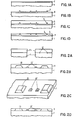
- An aluminum layer 2 between 100 and 1000 nm thick is then applied to the silicon substrate 1. 1A shows a section of the structure at this stage of manufacture.
- a tempering step follows at temperatures between 350 and 400 ° C., the aluminum tips growing out of the aluminum layer 2.
- the aluminum tips are regularly distributed over the aluminum layer 2.
- Their density which is preferably in the order of one peak per 100 microns 2, it is determined by the boron doping of the substrate 1.
- the density of the aluminum spikes on the substrate varies by a factor of 6.
- the annealing time determines the height of the aluminum teeth.
- the target height is between about 1 and about 2 ⁇ m.
- the aluminum layer 2 and the aluminum prongs are anodically oxidized, the aluminum which is at a positive potential being treated in an electrolyte solution, for example consisting of a solution of ammonium pentaborate in ethylene glycol, at voltages of up to approximately 20 volts.
- FIG. 1B shows the structure present after the anodic oxidation, the spikes consisting of aluminum oxide being designated by the reference number 3 and the aluminum oxide layer produced from the aluminum layer 2 by the reference number 4.
- a layer 5, which contains a binder and magnetic particles, is spun onto the structure shown in FIG. 1B and then hardened.
- the binder in layer 5 preferably consists of an epoxy resin and typically an epoxy resin of the bisphenol A-epichlorohydrin type.
- the magnetic particles preferably consist of ⁇ -Fe 2 O 3 .
- the layer 5 is made so thick that it at least largely covers the aluminum oxide teeth 3.
- the structure at this stage is shown in Fig. 1C.
- layer 5 is ground down to such an extent that the tips of the aluminum oxide teeth are exposed and polished.
- 1D shows a cross section through a section of the finished magnetic disk which has been produced in this way.
- the uncritical step of the on-board doping can achieve that the aluminum spikes are both evenly distributed and - depending on the strength of the doping - have the correct areal density.
- the method is further advantageous in that the magnetic layer can be applied to very different substrates without having to forego any of the favorable properties.
- the abrasion-resistant component consists of the same material as in the known disks, but it is anchored much more firmly than in the known disks. Due to the special type of manufacture, the abrasion-resistant material does not have to accept a loss in hardness; on the contrary, the aluminum oxide teeth have Mohs hardness of up to 9.
- a layer consisting of aluminum and silicon or a layer consisting of aluminum and a layer consisting of silicon is applied to a single-crystalline silicon substrate, then annealed and then cooled again, with Sili cium (saturated with 5 x 10 18 aluminum atoms / cm 3 ) in the form of small pyramids on the substrate surface epitaxially.
- Sili cium saturated with 5 x 10 18 aluminum atoms / cm 3
- a mixture of the binder and the magnetic particles is applied as a layer, then hardened and finally ground off until the upper surface of the pyramids is exposed.
- the deposition of the silicon does not take place over the whole area, but only at active centers of the silicon crystal, since these centers have a high tendency to nucleation.
- the density of the active centers and thus the areal density of the pyramids can be controlled in a simple manner without the need to process the substrate by means of selectively acting process steps, for example with the aid of a mask. Rather, the area density is controlled by influencing the silicon distribution in the material applied to the substrate.
- the explanation of the center formation should be preceded by a few general comments.
- the saturation concentration of silicon in solid aluminum is 1.2% by weight.
- the saturation concentration of silicon in aluminum is only about 0.4% by weight higher, ie it is 1.6% by weight.
- the eutectic point of the AlSi system is at 577 ° C. In the liquid phase present at this temperature, the silicon concentration can rise to 12% by weight. If the aluminum saturated with silicon is cooled after the tempering, the silicon is precipitated. If active centers are present on the substrate surface, the silicon is preferably epitaxially deposited on these active centers when it cools slowly. With increasing cooling rate more and more silicon remains in the form of small crystallites, which consist of an intermetallic compound, in aluminum.
- active centers are formed wherever silicon is released from the single-crystalline silicon substrate. The distribution of these centers over the substrate surface is statistical (homogeneous); their number depends on how much the silicon concentration in the aluminum adjacent to the silicon substrate is below the saturation concentration. The number of active centers can thus be influenced by the composition and structure of the material applied to the substrate. Most active centers will arise when the material applied is made of pure aluminum.
- 2A shows a section of the structure that is then present. It is then tempered at a temperature between 400 and 480 ° C in an inert gas atmosphere. As shown in FIG. 2B, relatively few active centers 12 are formed. When cooling slowly (m 5 ° C./min.), Epitaxially relative growth then takes place on the silicon substrate 1 at the locations where the active centers 12 have formed large pyramids 13 on. It is also possible that, in addition to the pyramids 13, further, but significantly lower pyramids 13 'grow up. The structure then shown is shown in FIG. 2C.
- layer 11 is preferably made using a detached with nitric acid, hydrochloric acid and phosphoric acid containing acid mixture and thereby the surface of the substrate 1 and the pyramids 13 and 13 'exposed.
- 2D shows a section of the structure then present in a perspective representation.
- FIG. 2E shows a section of the magnetic disk after a layer 5, which has applied a binder, preferably an epoxy resin and magnetic particles, such as ⁇ -Fe203, is then hardened and finally abraded until the surfaces layer 5 and the silicon pyramids are coplanar.
- the magnetic disk shown in FIG. 2E embodies the one extreme case in which the number of silicon pyramids is relatively small. The other extreme case will be explained with reference to FIG. 3.
- FIG. 3A shows a section of a structure in which an aluminum layer 6 and a thin silicon layer 7 are applied to a silicon substrate 1.
- the thickness ratio of layers 6 and 7 is chosen approximately such that the amount by weight of silicon in layer 7 is approximately 1.2% of the total amount by weight of aluminum and silicon.
- the structure then present is heated to a temperature between 400 and 480 ° C. and annealed.
- the silicon diffuses from the layer 7 into the aluminum layer 6 to form a layer 8 containing aluminum and silicon. Since the aluminum at the interface with the silicon substrate 1 does not contain any silicon at the beginning of the annealing process, silicon from the silicon substrate 1 is eagerly detached from the aluminum , which creates a large number of active centers 12.
- 3B shows the result of the annealing in a schematic cross-sectional representation. If you leave that Then cool the structure slowly ( ⁇ 5 ° C./min.), So silicon is deposited epitaxially from the layer 8 at the active centers 12 to form small silicon pyramids 13 (see FIG. 3C).
- the height of the silicon pyramids 13 depends on the number of active centers and the annealing and cooling time on the absolute amount of silicon in the layer 8. Since the maximum soluble amount (saturation concentration in solid aluminum) has an upper limit of 1.6% regardless of the tempering temperature, the available amount of silicon can only be influenced by the thicknesses with which the layers 6 and 7 are applied.
- 3D shows a schematic perspective illustration of a section of the structure that is present when layer 8 has been detached, for example with the above-mentioned acid mixture.
- a layer 5 consisting of the binder, which is preferably an epoxy resin, and magnetic particles, such as e.g. ⁇ -Fe203, spin-coated.
- the gently rising flanks of the pyramids 13 are particularly advantageous since they have very little influence on the flow of the resin during spin coating.
- Layer 5 is then hardened and ground until the surface of layer 5 is coplanar with the surface of silicon pyramids 13.
- 3E shows the finished magnetic disk in a schematic cross-sectional illustration.
- the silicon pyramids 13 are practically part of the substrate 1; better anchoring of the abrasion-resistant material cannot be achieved at all.
- the hardness of the pyramids 13 is remarkable, it can be increased if necessary by the silicon is superficially converted into Si 3 N 4 .
- the silicon substrate is apart from the elevations, ie in the case of FIGS. 2E and 3E the silicon pyramids 13, smooth, so that no disturbances for the magnetic layer are to be expected.
- FIG. 4 is very similar to the embodiments discussed above, but which is produced using a method which differs considerably from those described above.
- the starting point is a weakly boron-doped silicon substrate 1.
- the silicon substrate 1 can be a silicon plate or a silicon layer which is applied, for example by means of sputtering, to a base which preferably consists of aluminum or an aluminum alloy, such as aluminum magnesium .
- the entire area of the silicon substrate 1 is provided with an arsenic doping which is so high that it amounts to 10 17 arsenic atoms / cm 3 at a depth of approximately 1 ⁇ m.
- the doping can be done by diffusion or ion implantation.
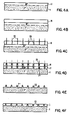
- the structure which then exists, in which only one surface has been doped with arsenic for the sake of simplicity, shows a detail in a schematic cross-sectional illustration in FIG.
- Layer 18 is made 2 to 3 ⁇ m thick.
- FIG. 4B The structure then shown is shown in FIG. 4B.
- the layer 18 is bombarded with high-energy heavy ions 19 with an energy of 5 to 20 MeV.
- latent traces 20 are generated in the layer 18, along which a local increase in the etching rate takes place. This local increase in the etching rate only occurs with insulating materials. It is a different damage mechanism than conventional ion implantation. No damage is generated in the underlying silicon.
- 10 5 Xe + ions / cm 2 are shot into the layer 18 on the order of magnitude. It is not necessary to provide measures, for example the provision of a mask, in order to achieve an even distribution of the tracks 20 over the layer 18.
- the layer 18 is selectively etched in the area of the tracks 20. If the layer 18 consists of a polyimide, it is preferably etched with a 1 to 2 molar KOH solution. The etching is very reproducible, and continuous channels 21 are formed, the diameter of which, depending on the etching conditions chosen, is between 0.5 and 1 gm.
- FIG. 4D Now about 10 16 boron atoms / cm 2 are implanted over the entire area with an energy of 130 KeV in the arsenic-doped layer 17, the layer having channels 21 18 serves as an implantation mask. The structure present after the implantation is shown in cross section in FIG. 4D. After ion implantation, layer 18 is completely removed.
- regions with a P + doping are produced by redistributing the boron ions by means of a high-temperature annealing step at the locations into which boron ions have been implanted.
- the silicon substrate is applied to a base consisting of aluminum or aluminum-magnesium, since high-temperature annealing for the boron distribution is then not possible, the boron implantation is carried out with continuously changing energy in the range between 20 and 260 KeV.
- the plate substrate is then etched in a hot solution containing 1 part pyrocatechol on 10 parts ethylenediamine, completely removing the N + regions.
- the P + -doped regions remain and form a matrix of elevations 23 distributed uniformly on the substrate.
- the elevations 23 are attacked during wet etching to such an extent that they have rounded edges, which increases their abrasion resistance in the finished magnetic plate and also for the flow behavior of the mixture containing the magnetic particles is advantageous in the subsequent coating by means of spin coating.
- the layer 5 which preferably consists of an epoxy resin and y-Fe 2 0 3 , has been spun on, its hardening and removal until its surface is coplanar with the tips of the elevations 23, the finished magnetic plate is present. A section of this magnetic disk is shown in FIG. 4F.
- the last-described method is particularly advantageous because, when it is used, the substrate is thin on a base from another Material applied silicon layer can be present because the silicon elevations are all generated at exactly the same height, so that grinding is not necessary to compensate for height differences and because a homogeneous distribution of the silicon elevations 23 on the substrate is achieved in a very simple manner.
- the magnetic disk produced which is shown in FIG. 4F, is considered to be very advantageous primarily because the abrasion-resistant material, ie the elevations 23, are optimally anchored in the silicon substrate and the round-etched corners of the elevations 23 prevent the magnetic head when it in the start / stop phase grinds on the plate, is damaged.
- a silicon plate is doped with boron so that the surface concentration is approximately 10 19 boron atoms / cm 3 . Then the silicon plate is vapor-deposited with an aluminum film which is approximately 500 nm thick. The vaporized silicon plate is annealed at approx. 350 ° C. for approx. 20 minutes, aluminum spikes, which are approximately 1 ⁇ m high, growing on. The aluminum film and the aluminum teeth are anodized. The anodic oxidation takes place in a bath which consists of a solution of ammonium pentaborate in ethylene glycol (17 g ammonium pentaborate per 100 ml ethylene glycol).
- a mixture of an epoxy resin based on bisphenol A-epichlorohydrin and ⁇ -Fe 2 O 3 is now spun onto the substrate. The coating is then polished and partially removed, exposing the aluminum oxide spikes and polishing.
- the density of the aluminum oxide spikes regularly distributed over the magnetic disk surface was in the order of 1 per 100 ⁇ m 2 .
- the magnetic disk thus produced was found to have excellent abrasion properties, and no particles were found on the magnetic disk surface even after prolonged use.
- a mixture consisting of epoxy resin based on bispenol A-epichlorohydrin and Y-Fe 2 0 3 was then applied to the substrate with the silicon pyramids existed, spun on, hardened and then polished until the top surface of the silicon pyramids was exposed.
- the silicon pyramids were evenly distributed over the disk substrate. Even after prolonged use, no silicon particles were found on the surface of the plate. Nevertheless, the abrasion resistance of the magnetic disk was not yet optimal, which was apparently due to the fact that the number of silicon pyramids was not high enough so that the magnetic head was not in constant contact with a silicon pyramid during the start / stop phase.
- the method used in this example differs from the method used in Example 2 only in that not an AlSi layer, but first an approximately 0.85 ⁇ m thick aluminum layer and then a 0.01 ⁇ m thick silicon layer is vapor-deposited. When the aluminum and silicon layers were detached, a large number of small silicon pyramids grown epitaxially on the silicon substrate were exposed. In the magnetic disk produced in this example, the magnetic layer, after it had been polished to such an extent that the tips of the silicon pyramids were exposed, was so thin and the number of silicon pyramids so large that the disk produced no longer met the specifications cations corresponded. However, the distribution of the silicon pyramids in this plate was homogeneously distributed over the plate substrate.
- the procedure used in this example differs from the previous two only in the manner in which the aluminum and silicon are applied. Namely, a 0.4 ⁇ m thick aluminum layer was applied, then a 0.01 ⁇ m thick silicon layer and finally a 0.45 ⁇ m thick aluminum layer was applied to the silicon substrate.
- the magnetic disk produced in this example met the requirements in every respect: the number of silicon pyramids produced was of the order of 10 5 / cm 2 , the pyramids were regularly distributed over the magnetic disk substrate, the magnetic layer had, after having been polished to such an extent that the tips of the The pyramids were exposed, the correct height (approx. 1 ⁇ m), the abrasion resistance of the magnetic disk was excellent, and no silicon particles were found on the magnetic disk surface even after prolonged use.
- a P -doped silicon plate substrate was provided with arsenic doping of 10 19 atoms / cm 3 (surface concentration) over the entire surface, the arsenic concentration at 1 ⁇ m depth being 10 17 atoms / cm 3 .
- the Dotie Unilateral implantation The surface of the arsenic-doped layer was coated with an approximately 2.5 ⁇ m thick layer of polyimide.
- the polyimide layer was bombarded with xenon ions at a dose of 10 5 ions / cm 2 and an energy of approximately 10 MeV.
- the polyimide was then exposed to an approximately 2 molar KOH solution, etching through channels with a diameter of approximately 0.5 to approximately 1 ⁇ m. Boron ions were then into the silicon substrate Tomen with a dose of 10 16 A / cm 2 is implanted with an energy of 130 keV, wherein the channeled polyimide layer serving as an implantation mask. In the next process step, the polyimide layer was completely removed by further etching in the approximately 2 molar KOH solution. This was followed by a tempering step at 900 ° C to redistribute the implanted boron.
- the entire area of the silicon plate substrate was then etched in a hot ethylenediamine-pyrocatechol solution (10 parts by weight of ethylenediamine to 1 part of pyrocatechol), the arsenic-doped areas having been completely removed.
- the P + regions generated during the redistribution of the implanted boron remained unetched except for a rounding of the edges and formed a matrix of elevations regularly distributed over the silicon plate substrate.
- the bumps had a height of approximately 1 ⁇ m and a density of approximately 10 5 bumps / cm 2 .
- a mixture of epoxy resin based on bispenol A-epichlorohydrin and ⁇ -Fe 2 O 3 was spun onto the silicon plate substrate thus formed and then polished off until the layer was coplanar with the upper surfaces of the silicon bumps.
- the disk thus produced had excellent abrasion properties, a completely smooth surface, and no silicon particles were found on the magnetic disk surface even after prolonged use.
Landscapes
- Chemical & Material Sciences (AREA)
- Inorganic Chemistry (AREA)
- Engineering & Computer Science (AREA)
- Metallurgy (AREA)
- Magnetic Record Carriers (AREA)
- Manufacturing Of Magnetic Record Carriers (AREA)
Priority Applications (4)
| Application Number | Priority Date | Filing Date | Title |
|---|---|---|---|
| EP84113055A EP0179934B1 (fr) | 1984-10-31 | 1984-10-31 | Disque magnétique et procédé pour sa fabrication |
| DE8484113055T DE3470811D1 (en) | 1984-10-31 | 1984-10-31 | Magnetic disc and process for producing it |
| JP60177788A JPS61129732A (ja) | 1984-10-31 | 1985-08-14 | 磁気デイスク及びその製造方法 |
| US06/782,839 US4689260A (en) | 1984-10-31 | 1985-10-02 | Abrasion-resistant magnetic recording disk |
Applications Claiming Priority (1)
| Application Number | Priority Date | Filing Date | Title |
|---|---|---|---|
| EP84113055A EP0179934B1 (fr) | 1984-10-31 | 1984-10-31 | Disque magnétique et procédé pour sa fabrication |
Publications (2)
| Publication Number | Publication Date |
|---|---|
| EP0179934A1 true EP0179934A1 (fr) | 1986-05-07 |
| EP0179934B1 EP0179934B1 (fr) | 1988-04-27 |
Family
ID=8192251
Family Applications (1)
| Application Number | Title | Priority Date | Filing Date |
|---|---|---|---|
| EP84113055A Expired EP0179934B1 (fr) | 1984-10-31 | 1984-10-31 | Disque magnétique et procédé pour sa fabrication |
Country Status (4)
| Country | Link |
|---|---|
| US (1) | US4689260A (fr) |
| EP (1) | EP0179934B1 (fr) |
| JP (1) | JPS61129732A (fr) |
| DE (1) | DE3470811D1 (fr) |
Families Citing this family (13)
| Publication number | Priority date | Publication date | Assignee | Title |
|---|---|---|---|---|
| DE8704667U1 (de) * | 1987-03-28 | 1987-07-30 | Basf Ag, 6700 Ludwigshafen | Magnetaufzeichnungsträger zu Testzwecken, insbesondere zur Eichung von Flug-Magnetköpfen |
| US5047274A (en) * | 1987-09-28 | 1991-09-10 | Noboru Tsuya | Annodized aluminum substrate for a magnetic recording disk in which pores are filled with a non magnetic material and the surface polished and etched |
| US4935278A (en) * | 1988-04-28 | 1990-06-19 | International Business Machines Corporation | Thin film magnetic recording disk and fabrication process |
| US5470636A (en) * | 1991-03-15 | 1995-11-28 | Yamaha Corporation | Magnetic recording medium and method of producing it |
| US5768075A (en) * | 1991-12-17 | 1998-06-16 | Baradun R&D Ltd. | Disk medium w/magnetically filled features aligned in rows and columns |
| WO1993012520A1 (fr) * | 1991-12-17 | 1993-06-24 | Certus Magnetics | Disque magnetique comportant des surfaces a structures etudiees et une rugosite controlee; procede de fabrication associe |
| JP2769420B2 (ja) * | 1992-05-01 | 1998-06-25 | インターナショナル・ビジネス・マシーンズ・コーポレイション | 磁気モーメント低下方法及びデータ記憶装置 |
| US5591502A (en) * | 1992-06-16 | 1997-01-07 | Shin-Etsu Chemical Co., Ltd. | Magnetic recording medium |
| US5582897A (en) * | 1993-09-10 | 1996-12-10 | Shin-Etsu Chemical Co., Ltd. | Magnetic recording medium |
| US5923511A (en) * | 1995-05-26 | 1999-07-13 | International Business Machines Corporation | Directly contactable disk for vertical magnetic data storage |
| US20040038082A1 (en) * | 2002-08-26 | 2004-02-26 | Toshihiro Tsumori | Substrate for perpendicular magnetic recording hard disk medium and method for producing the same |
| JP4436175B2 (ja) * | 2004-04-05 | 2010-03-24 | 信越化学工業株式会社 | 金属メッキ層付き単結晶Si基板 |
| WO2010067830A1 (fr) * | 2008-12-09 | 2010-06-17 | Hoya株式会社 | Support d’enregistrement magnétique et procédé de production d’un support d’enregistrement magnétique |
Citations (2)
| Publication number | Priority date | Publication date | Assignee | Title |
|---|---|---|---|---|
| FR2096031A5 (fr) * | 1970-06-08 | 1972-02-11 | Ibm | |
| US4393110A (en) * | 1981-03-07 | 1983-07-12 | Tdk Electronics Co., Ltd. | Magnetic recording medium |
Family Cites Families (5)
| Publication number | Priority date | Publication date | Assignee | Title |
|---|---|---|---|---|
| US2501126A (en) * | 1946-10-18 | 1950-03-21 | Indiana Steel Products Co | Magnetic record medium |
| JPS55125536A (en) * | 1979-03-16 | 1980-09-27 | Fuji Photo Film Co Ltd | Recording medium for vertical magnetic record |
| JPS5671821A (en) * | 1979-11-14 | 1981-06-15 | Hitachi Ltd | Substrate for magnetic disc and its manufacture |
| CA1188796A (fr) * | 1981-04-14 | 1985-06-11 | Kenji Yazawa | Support d'enregistrement magnetique |
| JPS59175033A (ja) * | 1983-03-23 | 1984-10-03 | Hitachi Ltd | 磁気デイスク |
-
1984
- 1984-10-31 EP EP84113055A patent/EP0179934B1/fr not_active Expired
- 1984-10-31 DE DE8484113055T patent/DE3470811D1/de not_active Expired
-
1985
- 1985-08-14 JP JP60177788A patent/JPS61129732A/ja active Granted
- 1985-10-02 US US06/782,839 patent/US4689260A/en not_active Expired - Fee Related
Patent Citations (2)
| Publication number | Priority date | Publication date | Assignee | Title |
|---|---|---|---|---|
| FR2096031A5 (fr) * | 1970-06-08 | 1972-02-11 | Ibm | |
| US4393110A (en) * | 1981-03-07 | 1983-07-12 | Tdk Electronics Co., Ltd. | Magnetic recording medium |
Non-Patent Citations (3)
| Title |
|---|
| EXTENDED ABSTRACTS, Band 83, Nr. 2, 1983, Seiten 490-491, Nr. 311, Pennington, N.J., US; W. LARSON u.a.: "Groove refill isolation for submicrometer devices" * |
| IBM TECHNICAL DISCLOSURE BULLETIN, Band 25, Nr. 11B, April 1983, Seiten 6114-6115, New York, US; W.E. MUTTER: "Selective filling of isolation trenches in silicon" * |
| PATENTS ABSTRACTS OF JAPAN, Band 5, Nr. 196 (P-93)[868], 12. Dezember 1981; & JP - A - 56 119 934 (TOKYO DENKI KAGAKU KOGYO K.K.) 19.09.1981 * |
Also Published As
| Publication number | Publication date |
|---|---|
| JPH0259523B2 (fr) | 1990-12-12 |
| US4689260A (en) | 1987-08-25 |
| EP0179934B1 (fr) | 1988-04-27 |
| JPS61129732A (ja) | 1986-06-17 |
| DE3470811D1 (en) | 1988-06-01 |
Similar Documents
| Publication | Publication Date | Title |
|---|---|---|
| EP0179934B1 (fr) | Disque magnétique et procédé pour sa fabrication | |
| DE69204940T2 (de) | Mit Diamant überzogener, gegossener Feldemissions-Elektronenemitter und Verfahren zur Herstellung desselben. | |
| EP0016404B1 (fr) | Support d'enregistrement magnétique et procédé pour sa fabrication | |
| DE69329635T3 (de) | Halbleiteranordnung und Verfahren zu ihrer Herstellung | |
| DE3707522C2 (fr) | ||
| DE1952626A1 (de) | Verfahren zur Herstellung von Isolationsschichten auf Halbleitersubstraten | |
| DE2258444A1 (de) | Verfahren und herstellung von elektrischisolierenden zonen in optischen bauelementen | |
| DE3203918C2 (de) | Magnetisches Aufzeichnungsmedium | |
| DE2523307C2 (de) | Halbleiterbauelement | |
| EP0076544A1 (fr) | Modulateur magnéto-optique | |
| DE2951287A1 (de) | Verfahren zur herstellung von ebenen oberflaechen mit feinsten spitzen im mikrometer-bereich | |
| DE3217026C2 (fr) | ||
| DE2729486A1 (de) | Verfahren zur herstellung einer magnetischen duennschicht | |
| EP0256278A1 (fr) | Disque magnétique et son procédé de mise en oeuvre | |
| DE69014787T2 (de) | Herstellungsverfahren von polaren Stücken und der Spalte von Dünnschicht-Magnetköpfen zur Informationsverarbeitungs-, Audio- oder Videoverwendung. | |
| EP0005744B1 (fr) | Procédé de croissance de couches épitaxiales sur des substrats en silicium, sélectivement dopés à haute concentration d'impureté | |
| DE69102173T2 (de) | Verfahren zur Herstellung eines Magnetkopfes. | |
| DE2517252A1 (de) | Halbleiterelement | |
| DE112013001656T5 (de) | Verbessertes Implantationsverfahren zur Bildung von Zerbrechlichkeit von Substraten | |
| DE3882856T2 (de) | Herstellung einer polykristallinen Schicht. | |
| DE3217550C2 (de) | Verfahren zum Herstellen einer ionenimplantierten Schicht eines Magnetblasenspeicher-Bauelements | |
| DE19747775C2 (de) | Röntgenstrahlenabsorber in einer Röntgenstrahlenmaske und Verfahren zur Herstellung desselben | |
| DE3839210A1 (de) | Verfahren zum axialen einstellen der traegerlebensdauer | |
| DE3301479A1 (de) | Verfahren zum herstellen eines halbleiterelementes | |
| DE3885446T2 (de) | Verfahren zur herstellung magnetischer aufzeichnungsträger. |
Legal Events
| Date | Code | Title | Description |
|---|---|---|---|
| PUAI | Public reference made under article 153(3) epc to a published international application that has entered the european phase |
Free format text: ORIGINAL CODE: 0009012 |
|
| AK | Designated contracting states |
Kind code of ref document: A1 Designated state(s): DE FR GB |
|
| 17P | Request for examination filed |
Effective date: 19860819 |
|
| 17Q | First examination report despatched |
Effective date: 19870213 |
|
| GRAA | (expected) grant |
Free format text: ORIGINAL CODE: 0009210 |
|
| AK | Designated contracting states |
Kind code of ref document: B1 Designated state(s): DE FR GB |
|
| GBT | Gb: translation of ep patent filed (gb section 77(6)(a)/1977) | ||
| REF | Corresponds to: |
Ref document number: 3470811 Country of ref document: DE Date of ref document: 19880601 |
|
| ET | Fr: translation filed | ||
| PLBE | No opposition filed within time limit |
Free format text: ORIGINAL CODE: 0009261 |
|
| STAA | Information on the status of an ep patent application or granted ep patent |
Free format text: STATUS: NO OPPOSITION FILED WITHIN TIME LIMIT |
|
| 26N | No opposition filed | ||
| PGFP | Annual fee paid to national office [announced via postgrant information from national office to epo] |
Ref country code: GB Payment date: 19920925 Year of fee payment: 9 |
|
| PGFP | Annual fee paid to national office [announced via postgrant information from national office to epo] |
Ref country code: DE Payment date: 19921027 Year of fee payment: 9 |
|
| PGFP | Annual fee paid to national office [announced via postgrant information from national office to epo] |
Ref country code: FR Payment date: 19931004 Year of fee payment: 10 |
|
| PG25 | Lapsed in a contracting state [announced via postgrant information from national office to epo] |
Ref country code: GB Effective date: 19931031 |
|
| GBPC | Gb: european patent ceased through non-payment of renewal fee |
Effective date: 19931031 |
|
| PG25 | Lapsed in a contracting state [announced via postgrant information from national office to epo] |
Ref country code: DE Effective date: 19940701 |
|
| PG25 | Lapsed in a contracting state [announced via postgrant information from national office to epo] |
Ref country code: FR Effective date: 19950630 |
|
| REG | Reference to a national code |
Ref country code: FR Ref legal event code: ST |