EP0179980B1 - Procédé de formation de marques d'alignement dans un corps semi-conducteur - Google Patents
Procédé de formation de marques d'alignement dans un corps semi-conducteur Download PDFInfo
- Publication number
- EP0179980B1 EP0179980B1 EP85106820A EP85106820A EP0179980B1 EP 0179980 B1 EP0179980 B1 EP 0179980B1 EP 85106820 A EP85106820 A EP 85106820A EP 85106820 A EP85106820 A EP 85106820A EP 0179980 B1 EP0179980 B1 EP 0179980B1
- Authority
- EP
- European Patent Office
- Prior art keywords
- layer
- alignment mark
- scribed
- semiconductor body
- alignment
- Prior art date
- Legal status (The legal status is an assumption and is not a legal conclusion. Google has not performed a legal analysis and makes no representation as to the accuracy of the status listed.)
- Expired
Links
Images

Classifications
-
- H—ELECTRICITY
- H10—SEMICONDUCTOR DEVICES; ELECTRIC SOLID-STATE DEVICES NOT OTHERWISE PROVIDED FOR
- H10W—GENERIC PACKAGES, INTERCONNECTIONS, CONNECTORS OR OTHER CONSTRUCTIONAL DETAILS OF DEVICES COVERED BY CLASS H10
- H10W46/00—Marks applied to devices, e.g. for alignment or identification
-
- H—ELECTRICITY
- H10—SEMICONDUCTOR DEVICES; ELECTRIC SOLID-STATE DEVICES NOT OTHERWISE PROVIDED FOR
- H10P—GENERIC PROCESSES OR APPARATUS FOR THE MANUFACTURE OR TREATMENT OF DEVICES COVERED BY CLASS H10
- H10P34/00—Irradiation with electromagnetic or particle radiation of wafers, substrates or parts of devices
- H10P34/40—Irradiation with electromagnetic or particle radiation of wafers, substrates or parts of devices with high-energy radiation
- H10P34/42—Irradiation with electromagnetic or particle radiation of wafers, substrates or parts of devices with high-energy radiation with electromagnetic radiation, e.g. laser annealing
-
- H—ELECTRICITY
- H10—SEMICONDUCTOR DEVICES; ELECTRIC SOLID-STATE DEVICES NOT OTHERWISE PROVIDED FOR
- H10W—GENERIC PACKAGES, INTERCONNECTIONS, CONNECTORS OR OTHER CONSTRUCTIONAL DETAILS OF DEVICES COVERED BY CLASS H10
- H10W46/00—Marks applied to devices, e.g. for alignment or identification
- H10W46/301—Marks applied to devices, e.g. for alignment or identification for alignment
-
- H—ELECTRICITY
- H10—SEMICONDUCTOR DEVICES; ELECTRIC SOLID-STATE DEVICES NOT OTHERWISE PROVIDED FOR
- H10W—GENERIC PACKAGES, INTERCONNECTIONS, CONNECTORS OR OTHER CONSTRUCTIONAL DETAILS OF DEVICES COVERED BY CLASS H10
- H10W46/00—Marks applied to devices, e.g. for alignment or identification
- H10W46/501—Marks applied to devices, e.g. for alignment or identification for use before dicing
-
- Y—GENERAL TAGGING OF NEW TECHNOLOGICAL DEVELOPMENTS; GENERAL TAGGING OF CROSS-SECTIONAL TECHNOLOGIES SPANNING OVER SEVERAL SECTIONS OF THE IPC; TECHNICAL SUBJECTS COVERED BY FORMER USPC CROSS-REFERENCE ART COLLECTIONS [XRACs] AND DIGESTS
- Y10—TECHNICAL SUBJECTS COVERED BY FORMER USPC
- Y10S—TECHNICAL SUBJECTS COVERED BY FORMER USPC CROSS-REFERENCE ART COLLECTIONS [XRACs] AND DIGESTS
- Y10S438/00—Semiconductor device manufacturing: process
- Y10S438/975—Substrate or mask aligning feature
Definitions
- This invention relates to a method of forming alignment marks in a semiconductor body and particularly to a fixture-less process employing a laser beam for scribing an alignment mark on the back side of a wafer having a heavily doped interior layer in which microscopic defects are induced by the laser beam and, then, heating the wafer to cause the defects to propagate to the front side of a wafer where they appear as an identically positioned image of the alignment mark scribed on the back side.
- U.S. Patent 3,752,589 discloses an optical-mechanical means and method for aligning the pattern of a photographic mask on one side of a wafer to a pattern on the opposite side, wherein individual optical images of the patterns on both sides of the wafer are obtained and, then, the position of the mask is mechanically adjusted until the two optical images are aligned.
- U.S. Patent 4,046,985 discloses an optical-mechanical semiconductor wafer alignment apparatus for repeatedly aligning the back sides of wafers to the axis of a kerf-cutting laser.
- a transparent mask having on its front side a duplicate of the device pattern and of the alignment marks on the opaque wafers, is visually aligned to the laser, and the apparatus is set to maintain this alignment.
- subsequently inserted opaque semiconductor wafers having the same alignment marks, will travel through the apparatus along the same path as the transparent mask, including inversion of the wafers, so that their back sides are aligned to the laser whose beam automatically impinges on the kerf areas between the devices.
- U.S. Patent 4,318,752 discloses a method of forming a p-doped area in an n-doped layer of a plural layer semiconductor body by passing a laser beam through a first p-doped layer into an adjacent n-layer which absorbs the laser beam energy and generates heat to cause diffusion of the p-doped layer into the n-doped layer.
- the wavelength of the laser beam is chosen such that it passes through the p-doped layer without absorption.
- U.S. Patent 4,131,487 discloses a process for gettering a semiconductor wafer with a laser beam, wherein a laser beam is directed upon the back side of the wafer to create lattice damage and strain in the back side. Subsequent heating of the wafer releases the strain to attract mobile defects from the front side of the wafer to the back side.
- the invention as claimed is intended to provide a simple process for aligning the front and back sides of a semiconductor wafer without the need for an expensive and unwieldly mechanical alignment fixture or apparatus and without the need for a photoresist blocking mask during an etching step, so that alignment marks may be formed on sandwich structures or other structures where one side of the structure is covered or otherwise inaccessible for alignment procedures.
- the advantages of the invention are achieved by using a laser beam to scribe an alignment mark on the back side of the wafer.
- the wavelength of the laser beam is chosen such that it passes through the lightly doped wafer without absorption but is absorbed by a following heavily doped semiconductor layer to generate therein heat and resulting defects.
- the semiconductor wafer is then heated to cause the defects to migrate through a lightly doped epitaxial layer to the front surface thereof in which there is formed an identically positioned image of the mark scribed on the back side.
- a surprisingly large number of applications require the precise alignment of a photoresist mask to both the front and back surfaces of a silicon wafer.
- silicon transducers and other micro-mechanical applications of silicon see "Silicon as a Mechanical Material", K. E. Petersen, Proceedings of the IEEE, May 1982, pages 420-457. Silicon is suitable for such micro-mechanical devices because the yield strength of silicon is 2.5 times that of stainless steel.
- double-sided alignment is being accomplished by aligning a contact mask to one side of the silicon wafer and, then, locking the wafer into position by means of a mechanical fixture.
- a second contact mask is then aligned to the first mask by means of alignment marks located at the edges of both masks. Once aligned, the entre assembly is clamped, and the exposure of the photoresist takes place.
- the problem with this approach is that it is extremely labor intensive, requires a significant amount of handling, is slow and not adaptable to automation, and cannot take advantage of modern projection printing tools.
- the invention is a relatively simple process which eliminates all of the foregoing problems and which can be implemented with existing equipment.
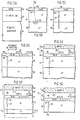
- Figures 1 and 2 show silicon wafers 10 and 12 being scribed on their back sides 14 and 16, respectively, by means of laser beams 18 and 20. In both cases, the laser beams are shown inclined at an angle for clarity of illustration, but, in practice the beams impinge at normal incidence to the planar back surfaces of the wafers. The difference between the two wafers is that wafer 12 ( Figure 2) contains a buried P + or N + layer 22 immediately above the lightly doped substrate 24, while wafer 10 does not. In the case of bipolar transistor fabrication, the heavily doped layer 22 corresponds to a buried isolation or (blanket) subcollector. For micro-mechanical structures, layer 22 might correspond to the typical boron etch stop, usually a blanket.
- the wavelength of the laser beam is selected to be in the near infrared band beyond the band edge of intrinsic silicon. (Such a wavelength can be obtained by merely removing the detachable frequency doubler from a conventional scribing laser). Thus, typically the shortest practical wavelength would be 1.1 pm, and the longest practical wavelength would be determined by the required resolution.
- the electromagnetic flux from the laser beam is dissipated as heat in the back sides of the wafers to form the characteristic scribe marks 26 and 28.
- the remaining flux continues into the lightly doped wafer substrate which is essentially transparent to the chosen laser wavelength.
- the laser beam continues through the remaining lightly doped layer of silicon until it hits the vacuum chuck 28 where it is either harmlessly dissipated or reflected back through and out of the wafer.
- Figure 2 which illustrates the first step of the invention, the laser beam 20 strikes the heavily doped region 22 where the flux couples to the free carriers produced by the high doping concentration, with a resultant increase in this region's absorption coefficient by a factor of three orders of magnitude.
- the heavily doped layer 22 is typically two or three ⁇ m thick, the absorbed power density rises dramatically, and enough so as to generate microscopic defects 29 in this layer. At this point, an alignment mark exists only on the back side 16 of the wafer 12 at the point 26. However, if the wafer is then heated, then, in a manner reminiscent of "secret ink", the scribing appears on the front side of the wafer as shown in Figure 3. On the other hand, and as shown in Figure 4 for comparison, the wafer 10, without the heavily doped internal layer, even though subjected to the identical heat treatment, remains blank on its front side.
- the dividing line between "heavily" doped and "lightly” doped is 3xlO ll atoms of dopant per cubic centimeter.
- Typical thicknesses of the layers shown in Figures 1-4 are as follows:
- the process has several advantages. For example, in some fabrication procedures, the substrate 24 containing the laser-scribed alignment mark 26 may be removed. However, with this process the alignment mark is preserved at the top surface of the epi-layer 30.
- the presence of the induced defects in an heavily boron-doped layer 22 at the precise location of the laser-scribed alignment marks offers another advantage; that is, anisotropic etching (e.g., with an E.D.P. etchant) will occur only in those regions of the layers 22 and 30 which are defined by the induced defects, the remaining P + layer functioning as the normal etch stop.
- the heavily doped layer 22 with the laser-induced defects performs the function of a buried etch mask which, without the invention, requires a blocking mask to prevent the P + from occurring where it is desired to continue etching to provide etched alignment marks.
- the invention eliminates the need for the blocking mask.
- Figures 5A to 5G illustrate still another embodiment for providing alignment for sandwich structures where one side of the semiconductor body is covered and cannot be physically seen.
- a heavily doped substrate 40 having a lightly doped epi-layer 42 covered by a transparent oxide layer 44, for example.
- the laser beam 46 (Figure 5B) must be directed onto the top side where it passes through the thin, transparent oxide layer 44 and layer 42 whose top surface is, thus, optically exposed, scribing alignment marks 48 and 50 in the top surfaces of layers 44 and 42, respectively, and inducing defects 52 in the heavily doped substrate 40.
- Figure 5C shows the migration path 54 of the defects upon the application of heat (which may occur during a normal annealing step); the defects migrate both upwardly to the top surface of the epi-layer 42 and also downwardly into the heavily doped substrate 40.
- a photoresist masking step is used to fabricate in the oxide layer 44 some structure 55, such as polysilicon, silicide or a device, using for mask alignment the scribed marks 48 and 50 or even the visible defects.
- This fabricated structure itself, forms another alignment feature.
- an opaque SOI (silicon-on-insulator) structure 56 is formed on top of the wafer by depositing a quartz insulating layer 58 to which another opaque silicon wafer 60 is bonded.
- the original substrate is removed by an isotropic, concentration-dependent etchant, such as HNA in the ratio of 1:3:8.
- the lightly doped epi-layer 42 acts as a substantially complete etch stop, without the invention there would be left a completely featureless, flat bottom surface without any alignment marks (the top surface having been covered by the opaque silicon wafer 60). However, with the invention this etchant continues etching into the lightly doped layer 42 to form therein an etched alignment mark 62 which can be used for aligning additional structures to the now-concealed structure 55.
Landscapes
- Exposure Of Semiconductors, Excluding Electron Or Ion Beam Exposure (AREA)
- Exposure And Positioning Against Photoresist Photosensitive Materials (AREA)
Claims (5)
Applications Claiming Priority (2)
| Application Number | Priority Date | Filing Date | Title |
|---|---|---|---|
| US06/620,644 US4534804A (en) | 1984-06-14 | 1984-06-14 | Laser process for forming identically positioned alignment marks on the opposite sides of a semiconductor wafer |
| US620644 | 1984-06-14 |
Publications (2)
| Publication Number | Publication Date |
|---|---|
| EP0179980A1 EP0179980A1 (fr) | 1986-05-07 |
| EP0179980B1 true EP0179980B1 (fr) | 1988-06-01 |
Family
ID=24486757
Family Applications (1)
| Application Number | Title | Priority Date | Filing Date |
|---|---|---|---|
| EP85106820A Expired EP0179980B1 (fr) | 1984-06-14 | 1985-06-03 | Procédé de formation de marques d'alignement dans un corps semi-conducteur |
Country Status (4)
| Country | Link |
|---|---|
| US (1) | US4534804A (fr) |
| EP (1) | EP0179980B1 (fr) |
| JP (1) | JPS613409A (fr) |
| DE (1) | DE3563148D1 (fr) |
Families Citing this family (39)
| Publication number | Priority date | Publication date | Assignee | Title |
|---|---|---|---|---|
| US4650524A (en) * | 1984-06-20 | 1987-03-17 | Sanyo Electric Co., Ltd | Method for dividing semiconductor film formed on a substrate into plural regions by backside energy beam irradiation |
| DE3683763D1 (de) * | 1986-03-27 | 1992-03-12 | Ibm Deutschland | Verfahren zur herstellung identisch angeordneter ausrichtmarkierungen auf gegenueberliegenden seiten einer halbleiterscheibe. |
| US4732867A (en) * | 1986-11-03 | 1988-03-22 | General Electric Company | Method of forming alignment marks in sapphire |
| JPH07107935B2 (ja) * | 1988-02-04 | 1995-11-15 | 株式会社東芝 | 半導体装置 |
| US4849365A (en) * | 1988-02-16 | 1989-07-18 | Honeywell Inc. | Selective integrated circuit interconnection |
| US5106432A (en) * | 1989-05-16 | 1992-04-21 | Oki Electric Industry Co., Ltd. | Wafer alignment mark utilizing parallel grooves and process |
| JPH0478123A (ja) * | 1990-07-20 | 1992-03-12 | Fujitsu Ltd | 半導体装置の製造方法 |
| JP3175188B2 (ja) * | 1991-05-10 | 2001-06-11 | ソニー株式会社 | 位置合わせマークの形成方法 |
| JPH07187892A (ja) * | 1991-06-28 | 1995-07-25 | Internatl Business Mach Corp <Ibm> | シリコン及びその形成方法 |
| US5580831A (en) * | 1993-07-28 | 1996-12-03 | Fujitsu Limited | Sawcut method of forming alignment marks on two faces of a substrate |
| JP3072005B2 (ja) * | 1994-08-25 | 2000-07-31 | シャープ株式会社 | 半導体装置及びその製造方法 |
| US5543365A (en) * | 1994-12-02 | 1996-08-06 | Texas Instruments Incorporated | Wafer scribe technique using laser by forming polysilicon |
| US5876819A (en) * | 1995-02-17 | 1999-03-02 | Mitsubishi Denki Kabushiki Kaisha | Crystal orientation detectable semiconductor substrate, and methods of manufacturing and using the same |
| US5828409A (en) * | 1995-06-30 | 1998-10-27 | Eastman Kodak Company | Film scanner mount assembly for a solid state sensor |
| US5904548A (en) * | 1996-11-21 | 1999-05-18 | Texas Instruments Incorporated | Trench scribe line for decreased chip spacing |
| US5843831A (en) * | 1997-01-13 | 1998-12-01 | Taiwan Semiconductor Manufacturing Company, Ltd. | Process independent alignment system |
| US5877064A (en) * | 1997-07-15 | 1999-03-02 | Taiwan Semiconductor Manufacturing Co.Ltd | Method for marking a wafer |
| US5985764A (en) * | 1997-12-22 | 1999-11-16 | Taiwan Semiconductor Manufacturing Company, Ltd. | Layer independent alignment system |
| US6760472B1 (en) * | 1998-12-14 | 2004-07-06 | Hitachi, Ltd. | Identification method for an article using crystal defects |
| US6710284B1 (en) * | 1999-02-26 | 2004-03-23 | Micron Technology, Inc. | Laser marking techniques for bare semiconductor die |
| SG106050A1 (en) * | 2000-03-13 | 2004-09-30 | Megic Corp | Method of manufacture and identification of semiconductor chip marked for identification with internal marking indicia and protection thereof by non-black layer and device produced thereby |
| US7157038B2 (en) * | 2000-09-20 | 2007-01-02 | Electro Scientific Industries, Inc. | Ultraviolet laser ablative patterning of microstructures in semiconductors |
| US6676878B2 (en) | 2001-01-31 | 2004-01-13 | Electro Scientific Industries, Inc. | Laser segmented cutting |
| US20060091126A1 (en) * | 2001-01-31 | 2006-05-04 | Baird Brian W | Ultraviolet laser ablative patterning of microstructures in semiconductors |
| CN1301178C (zh) * | 2001-01-31 | 2007-02-21 | 电子科学工业公司 | 半导体中微结构的紫外线激光烧蚀的图案化 |
| US6468704B1 (en) | 2001-04-16 | 2002-10-22 | Taiwan Semiconductor Manufacturing Company | Method for improved photomask alignment after epitaxial process through 90° orientation change |
| US6716723B2 (en) * | 2002-06-05 | 2004-04-06 | Intel Corporation | Wafer cutting using laser marking |
| US6596604B1 (en) | 2002-07-22 | 2003-07-22 | Atmel Corporation | Method of preventing shift of alignment marks during rapid thermal processing |
| KR101027568B1 (ko) * | 2007-09-25 | 2011-04-06 | 다이니폰 스크린 세이조우 가부시키가이샤 | 얼라인먼트 마크 형성 장치 |
| JP2010003939A (ja) * | 2008-06-23 | 2010-01-07 | Fujitsu Ltd | 基板の製造方法、基板の製造装置及び基板 |
| DE102009018653B4 (de) * | 2009-03-04 | 2015-12-03 | SolarWorld Industries Thüringen GmbH | Verfahren zur Herstellung von Halbleiterbauelementen unter Nutzung von Dotierungstechniken |
| US8148176B2 (en) * | 2009-08-20 | 2012-04-03 | Innovalight, Inc. | Methods for distinguishing a set of highly doped regions from a set of lightly doped regions on a silicon substrate |
| EP2378549A1 (fr) * | 2010-04-06 | 2011-10-19 | S.O.I.Tec Silicon on Insulator Technologies | Procédé de fabrication d'un substrat semi-conducteur |
| US9099481B2 (en) | 2013-03-15 | 2015-08-04 | Semiconductor Components Industries, Llc | Methods of laser marking semiconductor substrates |
| US9269607B2 (en) | 2014-06-17 | 2016-02-23 | Globalfoundries Inc. | Wafer stress control with backside patterning |
| RU2661977C1 (ru) * | 2014-07-03 | 2018-07-23 | Ниппон Стил Энд Сумитомо Метал Корпорейшн | Устройство лазерной обработки |
| GB201607589D0 (en) * | 2016-04-29 | 2016-06-15 | Nagravision Sa | Integrated circuit device |
| WO2022233720A1 (fr) | 2021-05-06 | 2022-11-10 | Ihp Gmbh - Innovations For High Performance Microelectronics / Leibniz-Institut Für Innovative Mikroelektronik | Dispositif à semi-conducteur doté d'un mécanisme de protection du côté arrière |
| CN119317122A (zh) * | 2024-12-16 | 2025-01-14 | 长飞先进半导体(武汉)有限公司 | 半导体器件及制造方法、功率模块、功率转换电路和车辆 |
Family Cites Families (13)
| Publication number | Priority date | Publication date | Assignee | Title |
|---|---|---|---|---|
| JPS5437474B1 (fr) * | 1968-06-10 | 1979-11-15 | ||
| US3752589A (en) * | 1971-10-26 | 1973-08-14 | M Kobayashi | Method and apparatus for positioning patterns of a photographic mask on the surface of a wafer on the basis of backside patterns of the wafer |
| US4174217A (en) * | 1974-08-02 | 1979-11-13 | Rca Corporation | Method for making semiconductor structure |
| US4046985A (en) * | 1974-11-25 | 1977-09-06 | International Business Machines Corporation | Semiconductor wafer alignment apparatus |
| JPS53108287A (en) * | 1977-03-03 | 1978-09-20 | Fujitsu Ltd | Manufacture of semiconductor device |
| US4137100A (en) * | 1977-10-26 | 1979-01-30 | Western Electric Company | Forming isolation and device regions due to enhanced diffusion of impurities in semiconductor material by laser |
| US4131487A (en) * | 1977-10-26 | 1978-12-26 | Western Electric Company, Inc. | Gettering semiconductor wafers with a high energy laser beam |
| US4217570A (en) * | 1978-05-30 | 1980-08-12 | Tektronix, Inc. | Thin-film microcircuits adapted for laser trimming |
| DE2829983A1 (de) * | 1978-07-07 | 1980-01-24 | Siemens Ag | Verfahren zum gettern von halbleiterbauelementen und integrierten halbleiterschaltkreisen |
| US4257827A (en) * | 1979-11-13 | 1981-03-24 | International Business Machines Corporation | High efficiency gettering in silicon through localized superheated melt formation |
| US4348809A (en) * | 1979-11-19 | 1982-09-14 | Wiltshire Cutlery Company Proprietary Limited | Combination sharpener device and scissors |
| US4318752A (en) * | 1980-05-16 | 1982-03-09 | Bell Telephone Laboratories, Incorporated | Heterojunction semiconductor laser fabrication utilizing laser radiation |
| US4415373A (en) * | 1981-11-17 | 1983-11-15 | Allied Corporation | Laser process for gettering defects in semiconductor devices |
-
1984
- 1984-06-14 US US06/620,644 patent/US4534804A/en not_active Expired - Fee Related
-
1985
- 1985-01-31 JP JP60015631A patent/JPS613409A/ja active Granted
- 1985-06-03 EP EP85106820A patent/EP0179980B1/fr not_active Expired
- 1985-06-03 DE DE8585106820T patent/DE3563148D1/de not_active Expired
Also Published As
| Publication number | Publication date |
|---|---|
| JPS613409A (ja) | 1986-01-09 |
| EP0179980A1 (fr) | 1986-05-07 |
| US4534804A (en) | 1985-08-13 |
| DE3563148D1 (en) | 1988-07-07 |
| JPH031820B2 (fr) | 1991-01-11 |
Similar Documents
| Publication | Publication Date | Title |
|---|---|---|
| US4534804A (en) | Laser process for forming identically positioned alignment marks on the opposite sides of a semiconductor wafer | |
| US3742230A (en) | Soft x-ray mask support substrate | |
| US5326426A (en) | Undercut membrane mask for high energy photon patterning | |
| US4732646A (en) | Method of forming identically positioned alignment marks on opposite sides of a semiconductor wafer | |
| EP0134438B1 (fr) | Tête à pointes à dépression et/ou électrostatique pour tenir des plaquettes semiconductrices ou autres composants électriques plans et méthode pour la fabriquer | |
| US3963489A (en) | Method of precisely aligning pattern-defining masks | |
| US5869386A (en) | Method of fabricating a composite silicon-on-insulator substrate | |
| EP0126621A2 (fr) | Marques d'alignement sur des plaquettes semi-conductrices et procédé pour fabriquer les marques | |
| US4680855A (en) | Electronic device manufacturing methods | |
| WO2004081992A2 (fr) | Plaquette semi-conductrice dotee de des de forme non rectangulaire | |
| GB2152690A (en) | Improvements in infra-red sensor arrays | |
| EP0554498A2 (fr) | Procédé de fabrication d'un substrat du type SOI comportant une couche mince uniforme de silicium | |
| JP2870492B2 (ja) | Soi基板およびその製造方法 | |
| JPS62283678A (ja) | 半導体装置の製造方法 | |
| JP3328975B2 (ja) | 半導体ウェーハ | |
| JPS56126914A (en) | Manufacture of semiconductor device | |
| Howard et al. | X-Ray Diffraction Microscopy of Planar Diffused Junction Structures | |
| JP3500813B2 (ja) | 半導体ウエハの切断方法 | |
| EP0494685B1 (fr) | Méthode de mesure du décalage d'un dessin | |
| US7029830B2 (en) | Precision and apertures for lithographic systems | |
| GB2115949A (en) | Silicon X-ray mask | |
| EP0424375A1 (fr) | Masque de canalisation monolithique ayant une construction de cristaux amorphes/monocristaux | |
| JPS63503425A (ja) | モノリシツクチヤンネルマスク | |
| US4352862A (en) | Thermally stable magnetic film which resists hard bubbles | |
| Aritsuka et al. | Development of LEEPL 6025 format mask blanks |
Legal Events
| Date | Code | Title | Description |
|---|---|---|---|
| PUAI | Public reference made under article 153(3) epc to a published international application that has entered the european phase |
Free format text: ORIGINAL CODE: 0009012 |
|
| AK | Designated contracting states |
Kind code of ref document: A1 Designated state(s): DE FR GB |
|
| 17P | Request for examination filed |
Effective date: 19860424 |
|
| 17Q | First examination report despatched |
Effective date: 19870716 |
|
| GRAA | (expected) grant |
Free format text: ORIGINAL CODE: 0009210 |
|
| AK | Designated contracting states |
Kind code of ref document: B1 Designated state(s): DE FR GB |
|
| REF | Corresponds to: |
Ref document number: 3563148 Country of ref document: DE Date of ref document: 19880707 |
|
| ET | Fr: translation filed | ||
| PLBE | No opposition filed within time limit |
Free format text: ORIGINAL CODE: 0009261 |
|
| STAA | Information on the status of an ep patent application or granted ep patent |
Free format text: STATUS: NO OPPOSITION FILED WITHIN TIME LIMIT |
|
| 26N | No opposition filed | ||
| PGFP | Annual fee paid to national office [announced via postgrant information from national office to epo] |
Ref country code: GB Payment date: 19920506 Year of fee payment: 8 |
|
| PGFP | Annual fee paid to national office [announced via postgrant information from national office to epo] |
Ref country code: FR Payment date: 19920601 Year of fee payment: 8 |
|
| PGFP | Annual fee paid to national office [announced via postgrant information from national office to epo] |
Ref country code: DE Payment date: 19920619 Year of fee payment: 8 |
|
| PG25 | Lapsed in a contracting state [announced via postgrant information from national office to epo] |
Ref country code: GB Effective date: 19930603 |
|
| GBPC | Gb: european patent ceased through non-payment of renewal fee |
Effective date: 19930603 |
|
| PG25 | Lapsed in a contracting state [announced via postgrant information from national office to epo] |
Ref country code: FR Effective date: 19940228 |
|
| PG25 | Lapsed in a contracting state [announced via postgrant information from national office to epo] |
Ref country code: DE Effective date: 19940301 |
|
| REG | Reference to a national code |
Ref country code: FR Ref legal event code: ST |