EP0180131B1 - Appareil de prise de vue en couleur avec compensation de porteur perdu - Google Patents
Appareil de prise de vue en couleur avec compensation de porteur perdu Download PDFInfo
- Publication number
- EP0180131B1 EP0180131B1 EP85113403A EP85113403A EP0180131B1 EP 0180131 B1 EP0180131 B1 EP 0180131B1 EP 85113403 A EP85113403 A EP 85113403A EP 85113403 A EP85113403 A EP 85113403A EP 0180131 B1 EP0180131 B1 EP 0180131B1
- Authority
- EP
- European Patent Office
- Prior art keywords
- frequency
- index
- output
- signal
- phase
- Prior art date
- Legal status (The legal status is an assumption and is not a legal conclusion. Google has not performed a legal analysis and makes no representation as to the accuracy of the status listed.)
- Expired
Links
- 238000003384 imaging method Methods 0.000 title claims description 23
- 230000004044 response Effects 0.000 claims description 19
- 238000010894 electron beam technology Methods 0.000 claims description 16
- 230000000306 recurrent effect Effects 0.000 claims description 11
- 230000003287 optical effect Effects 0.000 claims description 10
- 238000006243 chemical reaction Methods 0.000 claims description 5
- 230000000737 periodic effect Effects 0.000 claims description 4
- 238000010586 diagram Methods 0.000 description 13
- 230000004048 modification Effects 0.000 description 8
- 238000012986 modification Methods 0.000 description 8
- 230000001360 synchronised effect Effects 0.000 description 7
- 239000000969 carrier Substances 0.000 description 5
- 239000003990 capacitor Substances 0.000 description 3
- 238000010276 construction Methods 0.000 description 2
- 239000011159 matrix material Substances 0.000 description 2
- 230000010363 phase shift Effects 0.000 description 2
- 230000000630 rising effect Effects 0.000 description 2
- 241000526960 Amaranthus acanthochiton Species 0.000 description 1
- 239000003086 colorant Substances 0.000 description 1
- 230000008878 coupling Effects 0.000 description 1
- 238000010168 coupling process Methods 0.000 description 1
- 238000005859 coupling reaction Methods 0.000 description 1
- 230000003111 delayed effect Effects 0.000 description 1
- 238000001514 detection method Methods 0.000 description 1
- 238000009792 diffusion process Methods 0.000 description 1
- 239000000463 material Substances 0.000 description 1
- 229920003023 plastic Polymers 0.000 description 1
- 230000005855 radiation Effects 0.000 description 1
- 238000005070 sampling Methods 0.000 description 1
- 238000001429 visible spectrum Methods 0.000 description 1
Images


Classifications
-
- H—ELECTRICITY
- H04—ELECTRIC COMMUNICATION TECHNIQUE
- H04N—PICTORIAL COMMUNICATION, e.g. TELEVISION
- H04N5/00—Details of television systems
- H04N5/30—Transforming light or analogous information into electric information
-
- H—ELECTRICITY
- H04—ELECTRIC COMMUNICATION TECHNIQUE
- H04N—PICTORIAL COMMUNICATION, e.g. TELEVISION
- H04N9/00—Details of colour television systems
- H04N9/01—Circuitry for demodulating colour component signals modulated spatially by colour striped filters by phase separation
Definitions
- the present invention relates to a single-tube color imaging apparatus according to the preamble of claim 1.
- DE-B-27 37 925 discloses a color imaging apparatus of this type.
- the color image pickup tube of the known apparatus is provided with a color stripe filter comprising a plurality of successively arranged recurrent groups of different color stripes.
- An optical color image being focused on the target of the tube is converted to an electrostatic image, which is scanned line-by-line by an electron beam to produce a color-multiplexed video signal.
- Index stripes which are provided adjacent to the upper edge of a raster area are scanned by the electron beam at the beginning of a field for generating an index signal, the frequency of which is converted to a lower frequency and stored into a memory under the control of a read/write control circuit.
- the stored index signal is repeatedly read out of the memory at periodic intervals and fed to a frequency reconverter which converts the index signal to the original frequency.
- the reconverted index signal is fed to a demodulating circuit which additionally responds to the output of the target to derive color signals.
- the color-multiplexed video signal generated upon scanning of the electron beam across the target comprises a "carrier" having a frequency inversely proportional to the interval at which the recurrent groups of the filter are arranged, the carrier being modulated in phase with the individual stripes of each recurrent group and in amplitude with the intensity of element pictures of the incident image.
- the video signal is applied to a pair of synchronous detectors to which are also applied phase-shifted reference carriers. These reference carriers can be derived from the pickup tube as it is illuminated uniformly with light of a predetermined color and stored into a memory prior to operation of the imaging apparatus. If the actual image is wholly or partially dark, the color-multiplexed signal will lose the carrier component, resulting in a loss of synchronism in frequency and phase with the phase-shifted reference carriers.
- an optical image is focused on a photoelectrical conversion target of a color image pickup tube through a color stripe filter having a plurality of successively arranged recurrent groups of different color stripes and converted to an electrostatic image which is scanned line-by-line in rectangular raster form by an electron beam to generate a color-multiplexed video signal.
- the video signal comprises a carrier having a frequency inversely proportional to the intervals at which the recurrent groups are arranged, the carrier being modulated in phase with the individual color stripes of each recurrent group with respect to a reference phase and in amplitude with the intensity of elemental areas of the color image.
- the apparatus includes first and second index stripes adjacent to edges of a rectangular raster area of the target and scanned by the electron beam at periodic intervals for generating first and second index signals, respectively.
- the second index stripes are located in a portion of the target which is scanned at the beginning or end of each line.
- a memory is provided to store the first and second index signals and a carrier having a duration of at least one field which is derived from the target when it is uniformly illuminated by light of a predetermined color through the color filter during write mode.
- the memory is read during normal operation to generate first and second reference index signals and a reference carrier having the reference phase.
- a closed-loop controller is operable during the read mode to derive frequency and phase control signals from the reference index signals from the memory and those index signals from the index means and controls the frequency and phase relationships between the reference and modulated carriers in response to the control signals.
- a color demodulator derives color difference signals from the frequency-and-phase controlled carriers.
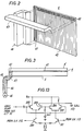
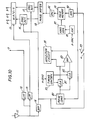
- a color imaging apparatus includes a color television pickup tube 1 having a pair of vertical and horizontal deflection yokes 2 and 3, a color stripe filter 4 affixed to the rear of a transparent faceplate 5 of an evacuated envelope 7, and a photoelectrical conversion target 6 attached to the rear of the filter 4 to be scanned by an electron beam emitted from an electron gun 8.
- a lens 9 focuses an object scene on the surface of the target 6 through the color filter 4.
- a video signal is read from the photoconductive layer of the conversion target 6 and applied to a preamplifier 11.
- Color filter 4 comprises a plurality of recurrent groups of stripes of a first color F1 (which may be one of the primary colors of blue, green and red), a second color F2 (which is cyan or magenta if F1 is blue, cyan or yellow if F1 is green, or yellow or magenta if F1 is red), and transparency for passing white light.
- F1 which may be one of the primary colors of blue, green and red
- F2 which is cyan or magenta if F1 is blue, cyan or yellow if F1 is green, or yellow or magenta if F1 is red
- transparency for passing white light These stripes have equal width and extend vertically throughout the target 6 and successively arranged across the horizontal dimension of the target 6 with the color stripes of each group recurring at intervals T.
- the filter 4 has therefore a spatial frequency inversely proportional to the periodic interval T.
- the color filter may comprise recurrent groups of stripes of red, green and blue of different widths with the groups being arranged at intervals T.
- Light passing through the color filter 4 is optically modulated by the striped color filter pattern and develops an electrostatic image on the conversion target 6 which is read by the electron beam scanned.
- Line-by-line rectangular raster scan is provided by the horizontal and vertical yokes 2 and 3 energized by sweep currents supplied from a deflection circuit 10.
- the first filter stripe F1 is green and the second stripe F2 is cyan.
- the light incident on the green stripes is removed of its red and blue components to allow its green component to pass to target 6, while the light incident on the cyan stripes is removed of the red component (R) to allow its green (G) and blue (B) components to pass to target 6.
- the color-multiplexed signal contains (G), (B + G) and (R + B + G) components derived respectively from stripes F1, F2 and W. Therefore, the video signal S obtained from the target 6 is given by: where, (where f 1 represents the frequency of the "carrier").
- the phase component ⁇ indicates a phase deviation from the reference phase of the "carrier” and represents the spatial difference between the individual filter stripes within each recurrent group, and the phase component ⁇ represents a phase deviation attributed to the nonlinearity of the deflection system.
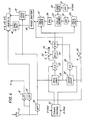
- the output of preamplifier 11 is applied to low-pass filters 12 and 13 and to a band-pass filter 14.
- Low-pass filter 12 having a cut-off frequency immediately below the carrier frequency f 1 passes the luminance component of the video signal to a luminance output terminal Y and low-pass filter 13 having a cut-off frequency much lower than the cut-off frequency of filter 12 passes the baseband of the video signal which is represented by the first term of Equation 1 to a matrix circuit 15.
- the "carrier" component of the video signal, represented by the second term of Equation 1 is passed through the band-pass filter 14 to first inputs of synchronous detectors 16 and 17.
- band-pass filter 14 is also applied through a mode select switch 20 and an analog-to- digital converter 21 to a field memory 22 and also to a frequency comparator 23 and a phase comparator 24.
- Comparators 23 and 24 compare the frequency and phase of the modulated carrier passing through the band-pass filter 14 with those of an output signal from a digital-to-analog converter 30 and supply their outputs to sample-and-hold circuits 25 and 26, respectively.
- Sample-and-hold circuits 25 and 26 are sampled by pulses derived in a timing control circuit 31 from vertical and horizontal sync pulses supplied from a vertical- and horizontal-sync generator 19.
- sample-and-hold 25 is sampled at the beginning of each "field" interval for storing a frequency difference signal until the end of the field and sample-and-hold 26 is sampled at the beginning of each horizontal line scan for storing a phase difference signal until the end of the line.
- These frequency and phase difference signals which will be derived in a manner as will be described later, drive a variable frequency oscillator 27 and a variable phase shifter 28 which are connected in series to an address generator 29 that addresses the field memory 22.
- a mode select switch 32 applies a reference voltage from voltage source 33 to the variable frequency oscillator 27 prior to normal imaging operation.
- the color filter 4 includes a horizontal band 40 of alternating opaque and transparent "field” index stripes successively arranged in an area outside of and adjacent to the upper edge of an image incident area 42 but within the rectangular raster area of the electron beam and a vertically extending band 41 of likewise opaque and transparent "line” index stripes arranged in a portion of the target 6 which is outside of and adjacent to the line-start edge of image incident area 42 but within the rectangular raster scan area.
- Image pickup tube 1 is preferably provided with a light guide 43 which is formed of a transparent plastic material to uniformly illuminate the "field” index stripes 40 with light from an external source.
- a second light guide 44 of identical construction uniformly illuminates the "line” index stripes 41 with external light. As shown in Fig.
- light guide 44 is constructed of a right-angled member having a parabolic internal reflecting bend 45 at which light from a light source 46 is reflected into parallel rays which are totally internally reflected at a surface 47 to the line index stripes 41.
- Light guide 44 is secured to one edge of the faceplate 5 of the image pickup tube in opposed relation to the line index stripes 41.
- light guide 43 is secured to the upper edge of the faceplate in opposed relation to the field index stripes 40.
- Index stripes 40 and 41 are illuminated both during write and read modes of field memory 22.
- Target 6 is scanned so that it develops a field index signal as the beam traverses field index stripes 40 and a line index signal as it traverses the line index stripes 41.
- the field index signal is generated at the beginning of each field interval prior to the generation of a "field” signal and the line index signal is generated at the beginning of each line scan prior to the generation of a "line” signal.
- switches 20 and 32 are manually turned to "write" position W and the target 6 is illuminated uniformly with light of a predetermined color to generate a "carrier" at frequency f, in addition to the field and line index signals, the carrier and index signals being digitized by A/D converter 21 and written into field memory 22.
- Variable frequency oscillator 27 is supplied with the reference voltage to generate constant-frequency clock pulses which drive the address generator 29 through variable phase shifter 28.
- Variable phase shifter 28 is adjusted so that it provides no phase shift when it receives zero voltage from sample-and-hold 26.
- field memory 22 is addressed at a constant rate by address generator 29 to write the index signals and the reference carrier.
- switches 20 and 32 are returned to "read" position R and the target 6 is illuminated with the optical image of an object to produce a signal which is a "carrier” modulated in amplitude with the intensity of picture elements of the image and in phase with the individual stripes of each recurrent group of the filter 4, as represented by the second term of Equation 1.
- the modulated carrier has a phase difference ⁇ with respect to the reference "carrier” stored in memory 22.
- Target 6 is also illuminated with an optical image formed by light rays passing through the field and line index bands 40 and 41 to produce field and line index signals, respectively.
- Frequency difference between the field index signal from band-pass filter 14 and the reference field index signal from D/A converter 30 is detected by frequency comparator 23 at the beginning of each field and stored in sample-and-hold circuit 25 until the end of that field.
- Phase difference between the line index signal from band-pass filter 14 and the reference line index signal from D/A converter 30 is detected by phase comparator 24 at the beginning of each scan line and stored in sample-and-hold circuit 26 until the end of that line scan.
- the stored frequency difference drives the variable frequency oscillator 27 so that address generator 29 is clocked at a constant rate that is determined by the frequency difference between the compared field index signals, so that the frequency of a modulated carrier that occurs in succession to the field index signal matches in frequency with the reference carrier read out of memory 22.
- the output of oscillator 27 is phase-controlled by variable phase shifter 28 in accordance with the phase difference stored in sample-and-hold circuit 26 and this phase compensation is repeated for each line.
- the reference carrier thus generated by the frequency and phase compensation is represented by sin( ⁇ t + 8).
- the nonlinearity phase component 8 represents the nonlinearity of the deflection system caused when the electron beam scans the field index stripes 40, this phase component being equal to the nonlinearity phase component of the modulated "carrier" generated during each line scan.
- the output of D/A converter 30 is fed to a phase shifter 18 where it is shifted in phase by +60° and -60° with respect to the modulated "carrier" and applied respectively to synchronous detectors 16 and 17.
- Color difference signals are produced by the synchronous detectors 16 and 17 and applied to color matrix circuit 15 where they are combined with the baseband of the color-multiplexed signal from low-pass filter 13 to generate primary color signals, which are applied to terminals R, G and B. It is seen therefore that in cases where the output of band-pass filter 14 contains little or no carrier component the frequency difference which may exist between the reference and present field index signals controls the variable frequency oscillator 27 instead of it being controlled with the frequency difference which might exist between the lost carrier and the reference carrier.
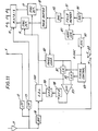
- FIG. 4 An embodiment shown in Fig. 4 is similar to the Fig. 1 embodiment except that it employs frequency converters 50 and 51 and a constant frequency oscillator 52.
- the reference carrier generated in the write mode is fed to the frequency converter 50.
- Frequency converter 50 essentially comprises a mixer which combines a constant frequency carrier from variable phase shifter 28 with signals from band-pass filter 14 passed through switch 20 during write mode to "beat down" their frequencies to produce lower-frequency "field and line” index signals and a lower-frequency reference carrier.
- the purpose of the frequency reduction is to reduce the memory capacity of field memory 22.
- Address generator 29 is clocked by oscillator 52 which is reset to a predetermined phase in response to a horizontal sync pulse to store the lower-frequency signals into field memory at a constant rate.
- field memory 22 is addressed at the same constant rate as in write mode.
- the output of D/A converter 30 is mixed with the output of variable phase shifter 28 to reconvert the frequencies of the signals read out of memory 22.
- the field and line reference index signals from frequency converter 51 are compared with the corresponding index signals from band-pass filter 14 by frequency and phase comparators 23 and 24 in a manner identical to that of Fig. 1 to control the variable frequency oscillator 27 and variable phase shifter 28.
- the frequency and phase of the locally oscillated carrier that is applied to frequency converter 51 are therefore controlled by the frequency difference between the reference field index signal and the corresponding field index signal from the target 6 and further controlled by the phase difference between the reference line index signal and the corresponding line index signal from the target.
- Frequency converter 51 reconverts or "beat up" the frequency of the output of D/A converter 30 to original frequency values in response to the frequency and phase differences, so that reference carrier output which is fed to phase shifter 18 from frequency converter 51 is matched in frequency and phase with the modulated carrier from band-pass filter 14.
- Fig. 5 is a modification of the Fig. 1 embodiment in which the frequency and phase of the modulated carrier are controlled by a deflection circuit 55 in response to the outputs of sample-and-hold circuits 25 and 26.
- the reference signals are written and read at constant rate determined by oscillator 56 as in the Fig. 4 embodiment.
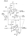
- Fig. 6 shows details of the deflection circuit 55.
- Deflection circuit 55 comprises a vertical deflection circuit 60V and a horizontal deflection circuit 60H of identical construction with different circuit parameters.
- Each of the deflection circuits includes a constant current source formed by a resistor R1 and a transistor Q1 connected in a series circuit with a switching transistor Q2 from a voltage supply Vcc to ground.
- the bases of transistors Q1V and Q1H are coupled together to a moving contact arm of a manually operated switch 64 and the bases of transistors Q2V and Q2H are biased by vertical and horizontal sync pulses, respectively.
- the read-write switch has a write terminal W impressed with a reference voltage by a voltage source 62 and a read terminal R to which the output of sample-and-hold 25 is applied.
- the collector-emitter path of transistor Q2 is in shunt with a storage capacitor C1 which charges through the constant current source when the transistor Q3 is nonconductive and discharges when the latter is biased conductive in response to the respective sync pulse.
- the voltage developed across the capacitor C1 biases a transistor Q3 which is in series with a resistor R2, forming a buffer amplifier. Voltages developed across resistors R2V and R2H are applied through coupling capacitors C2V and C2H to deflection yokes 2 and 3 respectively.
- Manually operated mode select switches 63V and 63H are ganged with switch 61.
- the read terminals R of switches 63V and 63H are coupled together to the output of sample-and-hold 26 and the write terminals W are impressed with beam centering reference voltages from voltage sources 64V and 64H, respectively.
- Each of the switches 63 has a moving contact arm which is coupled by a resistor R3 to the associated deflection yoke.
- switches 61, 63V, 63H are turned to write position W.
- the constant current source transistors Q1V and Q1H are biased at a reference potential to generate vertical and horizontal reference sweep voltages.
- the vertical and horizontal yokes are respectively impressed with the reference sweep voltages which are respectively summed with beam centering reference potentials which are determined so that the electron beam is exactly centered on the target,
- the target is then illuminated with light of a predetermined color in the same manner as in the previous embodiment to generate a "carrier" and applied through band-pass filter 14 and through switch 20 to A/D converter 21 and stored into field memory 22 at constant rate.
- the transistors Q1V and Q1 H are biased with an error voltage supplied from sample-and-hold 25 so that the vertical and horizontal sweep waveforms are adjusted in a direction tending to compensate for any variations in the deflection waveforms.
- the phase error signal from sample-and-hold 26 is applied to the yokes 2 and 3 to compensate for beam's deviation from the calibrated center position.
- Fig. 7 is an illustration of a further modification of the Fig. 1 embodiment.
- a variable delay line or a charge-coupled device 70 is employed and field memory 22 is addressed at constant rate by oscillator 71 during write and read modes.
- Delay line 70 is connected to the band-pass filter 14 to introduce a delay time to the modulated carrier before it is applied to synchronous detectors 16, 17 in response to the output of variable phase shifter 28.
- Frequency and phase comparators 23 and 24 take their first inputs from the output of variable delay line 70 and their second inputs from D/A converter 30 to supply their outputs through respective sample-and-holds to variable frequency oscillator 27 that drives the delay line 70 by way of variable phase shifter 28.
- the amount of time delay is therefore controlled with the frequency of the oscillator 27 and the timing of this delay is controlled with the phase shifter 28 in a feedback loop.
- the modulated carrier applied to synchronous detectors 16 and 17 is therefore matched in frequency and phase with those supplied from phase shifter 18.
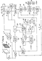
- Fig. 8 is an illustration of a second embodiment of the present invention in which line index signals are generated at the beginning and end of each line scan by line index bands 41 and 48 which extend vertically parallel to the line-start and line-end edges of image incident area 42, respectively, while the field index band 40 employed in the embodiments of Figs. 1, 4, 5 and 7 is dispensed with.
- first and second line index signals are generated respectively by the line index stripes 41 and 48 and stored with the reference carrier into memory 91 via switch 89 and A/D converter 90 at a constant rate determined by a voltage which is supplied from DC source 94 via switch 84 to variable frequency oscillator 85 which in turn clocks address generator 87 via variable phase shifter 86.
- a phase comparator 80 compares the modulated carrier from band-pass filter 14 with a reference carrier output from D/A converter 92.
- the output of phase comparator 80 is applied to sample-and-hold circuits 81 and 82.
- Sampling pulses for sample-and-hold circuits 81 and 82 are derived by a timing control circuit 93 from horizontal sync pulses so that sample-and-hold 81 is timed to sample a phase difference between a first line index signal developed at the beginning of each line scan from the line-start index band 41 and the corresponding reference line index signal read from memory 91 and sample-and-hold 82 is timed to sample a phase difference between a subsequent line index signal generated by the line-end index band 48 and the corresponding line index signal subsequently read from the memory.
- a differential amplifier 83 compares the phase difference values stored in sample-and-holds 81 and 82 with each other to detect a difference therebetween. This difference indicates a frequency variation of the modulated carrier as it experiences during a line scan, this being applied to variable frequency oscillator 85 via switch 84.
- Variable phase shifter 86 provides variable phase shift to the output of oscillator 85 in response to the phase-difference output from sample-and-hold 81.
- Address generator 87 is responsive to the output of variable phase shifter 86 for addressing field memory 91 at a variable rate which is controlled with the frequency variation detected by differential amplifier 83 and is phase-controlled with the phase difference stored in sample-and-hold 81.
- the signal from band-pass filter 14 is therefore matchedI ⁇ in frequency and phase with the signal read out of memory 91 even if the former lacks carrier information.
- Fig. 8 can be modified in various ways in like manner that the Fig. 1 embodiment is modified.
- the output of variable phase shifter 86 is coupled to frequency converters 95 and 96 for converting the frequencies of the line index signals and reference carrier to lower frequency values and reconverting them to original frequency values as these signals are read out of memory 91 which is addressed at a constant rate during both write and read modes by oscillator 97.
- Fig. 10 the outputs of differential amplifier 83 and sample-and-hold 81 are supplied to deflection circuit 55 of a circuit configuration identical to that shown in Fig. 6 and the field memory 91 is controlled at a constant rate during both write and read modes.
- Deflection circuit 55 operates in a manner identical to that described with reference to Fig. 6.
- variable frequency oscillator 98 the output of differential amplifier 83 is applied to variable frequency oscillator 98, the output of which is phase-controlled by variable phase shifter 99 with the output of sample-and-hold 81 and applied to CCD variable delay line 100 connected in the circuit between band-pass filter 14 and synchronous detectors 16,17.
- Field memory 91 is controlled at constant rate during both write and read modes.
- variable delay line 100 introduces a delay time to the modulated carrier in accordance with the frequency variation detected by differential amplifier 83.
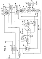
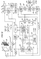
- Fig. 12 is an illustration of a third embodiment of the present invention which is intended to overcome the slow-response problem.
- the color filter 4 is provided with the field index band 40 and line index bands 41 and 48.
- Phase comparator 110 and frequency comparator 111 provides phase and frequency difference information to sample-and-holds 112, 113 and 114 which are controlled by a timing control circuit 115 so that the phase differences at the beginning and end of each line scan are stored in sample-and-holds 112 and 113 respectively and the frequency difference at the beginning of each field is stored in sample-and-hold 114.
- sample-and-holds 112 and 113 are fed to a variable-amplitude ramp generator 116 to cause it to generate a variable-amplitude ramp voltage having the line frequency.
- Sample-and-hold 114 controls the frequency of oscillator 118 through switch 117.
- Variable phase shifter 119 is controlled by a voltage developed in sample-and-hold 112 to phase-control the output of oscillator 118 and applies it to frequency converters 124 and 128.
- switch 121 After passing through switch 121, the frequencies of line index signals and reference carrier from band-pass filter 14 are converted to lower-frequency values by frequency converter 124 and stored through A/D converter 125 into field memory 126.
- Reference voltage from DC source 120 drives the oscillator 118 at a predetermined rate to supply a constant-frequency local-oscillator carrier via phase shifter 119 to frequency converter 124.
- Address generator 129 and oscillator 130 provide constant-rate write and read operations.
- Frequency converter 128 reconverts the output of D/A converter 127 to original frequency values in accordance with the output of variable phase shifter 119.
- the output of frequency converter 128 is applied to comparators 110 and 111 to permit the detection of the phase and frequency differences.
- band-pass filter 122 is also connected through a one-line delay line 122 to a voltage- controlled variable delay line 123.
- Delay line 123 has a phase control terminal connected to the output of sample-and-hold 112 and a frequency control terminal connected to the output of ramp generator 116.
- the ramp generator 116 comprises transistors 200 and 201 connected in a differential amplifier configuration.
- a horizontal ramp voltage is applied from the deflection circuit 10 to the bases of transistors 202, 203, 204 and 205 which are connected in a variable-gain, balanced amplifier configuration to the transistors 200 and 201.
- the amplitude of the horizontal ramp waveform is controlled by frequency variation represented by a voltage difference between the outputs of sample-and-holds 112 and 113 which is detected by transistors 200 and 201.
- the variable amplitude ramp voltage is taken from the collector of transistor 203 to the frequency control terminal of variable delay line 123, so that the modulated carrier is linearly increasingly delayed to the extent determined by the maximum amplitude of the applied horizontal ramp voltage.
- Sample-and-hold 112 determines the start timing of the linear delay.
- the frequency and phase of the modulated carrier are thus controlled by phase comparator 110 and frequency comparator 111 simultaneously with the frequency and phase control operation performed on the reference carrier.
- the delay which is inherently introduced to the reference carrier by the feedback loop is compensated for by the introduction of delay to the modulated carrier.
- Fig. 12 can be simplified as shown in Fig. 14 in which the color filter 4 is provided with only vertically extending index bands 41 and 48.
- a differential amplifier 130 is provided to detect the difference between the phase-difference values stored in sample-and-holds 112 and 113 in order to control the variable frequency oscillator 118.
- the light incident on the line index bands 41 and 48 tends to diffuse as it passes through the faceplate 5 of pickup tube and stray out of the intended path into the image incident area 42 with the result that the incident optical image is blurred at the opposite vertical edges of a viewing screen.
- Fig. 15 illustrates a block diagram of an embodiment useful for causing the electron beam to skip such boundary areas.
- a bipolar pulse generator 300 generates a pair of positiveand negative-going narrow pulses 302, Fig. 16, so that the positive-going pulse occurs immediately preceding the falling edge of a horizonal ramp voltage 303 generated by the horizontal sweep generator 60H, Fig. 6, and the negative-going pulse occurs immediately following that falling edge.
- Each of the bipolar pulses has a duration corresponding to the time the beam takes to move across each line index band.
- the bipolar pulses are combined in a summing circuit 301 with the horizonal ramp voltage 303 to produce a combined waveform 304 having a sharply falling peak that corresponds to the boundary between the line index band 41 and image incident area 42 and a sharply rising edge that corresponds to the boundary between the line index band 48 and the area 42.
- the falling and rising peaks cause the electron beam to skip these boundaries at higher speed that it scans across the image incident area.
Landscapes
- Engineering & Computer Science (AREA)
- Multimedia (AREA)
- Signal Processing (AREA)
- Color Television Image Signal Generators (AREA)
- Video Image Reproduction Devices For Color Tv Systems (AREA)
Claims (13)
Applications Claiming Priority (8)
| Application Number | Priority Date | Filing Date | Title |
|---|---|---|---|
| JP59222383A JPS61100085A (ja) | 1984-10-23 | 1984-10-23 | カラ−撮像装置 |
| JP222383/84 | 1984-10-23 | ||
| JP59228682A JPS61107889A (ja) | 1984-10-30 | 1984-10-30 | カラ−撮像装置 |
| JP228682/84 | 1984-10-30 | ||
| JP229751/84 | 1984-10-31 | ||
| JP59229751A JPS61108279A (ja) | 1984-10-31 | 1984-10-31 | カラ−撮像装置 |
| JP1984167944U JPS6183393U (fr) | 1984-11-07 | 1984-11-07 | |
| JP167944/84U | 1984-11-07 |
Publications (3)
| Publication Number | Publication Date |
|---|---|
| EP0180131A2 EP0180131A2 (fr) | 1986-05-07 |
| EP0180131A3 EP0180131A3 (en) | 1987-06-16 |
| EP0180131B1 true EP0180131B1 (fr) | 1989-09-20 |
Family
ID=27474163
Family Applications (1)
| Application Number | Title | Priority Date | Filing Date |
|---|---|---|---|
| EP85113403A Expired EP0180131B1 (fr) | 1984-10-23 | 1985-10-22 | Appareil de prise de vue en couleur avec compensation de porteur perdu |
Country Status (4)
| Country | Link |
|---|---|
| US (1) | US4736243A (fr) |
| EP (1) | EP0180131B1 (fr) |
| KR (1) | KR900002386B1 (fr) |
| DE (1) | DE3573204D1 (fr) |
Families Citing this family (10)
| Publication number | Priority date | Publication date | Assignee | Title |
|---|---|---|---|---|
| US4855816A (en) * | 1984-10-23 | 1989-08-08 | Victor Company Of Japan, Ltd. | Color imaging apparatus including phase control system for maintaining start positions of scanning lines equal to start positions of reference values thereof |
| US4857995A (en) * | 1984-10-23 | 1989-08-15 | Victor Company Of Japan, Ltd. | Color imaging apparatus including control system for stabilizing phase and frequency of a video signal carrier frequency |
| JPS6318891A (ja) * | 1986-07-11 | 1988-01-26 | Victor Co Of Japan Ltd | カラ−撮像装置 |
| EP0274820B1 (fr) * | 1986-10-15 | 1992-04-15 | Victor Company Of Japan, Limited | Caméra de télévision en couleurs |
| JPS6438890U (fr) * | 1987-09-02 | 1989-03-08 | ||
| US4974078A (en) * | 1989-11-13 | 1990-11-27 | Eastman Kodak Company | Digital compression method and system with improved coding efficiency |
| GB9620838D0 (en) | 1996-10-02 | 1996-11-20 | Marconi Gec Ltd | A camera |
| JP3559743B2 (ja) * | 1999-12-17 | 2004-09-02 | 日本オプネクスト株式会社 | 位相周波数同期回路および光受信回路 |
| US7298418B2 (en) * | 2004-02-06 | 2007-11-20 | Broadcom Corporation | Method and system for processing in a non-line locked system |
| JP4379380B2 (ja) * | 2005-04-28 | 2009-12-09 | ソニー株式会社 | 水平レジスタ転送パルス生成回路及び撮像装置 |
Family Cites Families (8)
| Publication number | Priority date | Publication date | Assignee | Title |
|---|---|---|---|---|
| FR2139179B1 (fr) * | 1971-05-26 | 1977-12-23 | Matsushita Electric Industrial Co Ltd | |
| US3755620A (en) * | 1972-06-30 | 1973-08-28 | Columbia Broadcasting Syst Inc | Single tube color television camera system and method |
| US4185296A (en) * | 1976-08-24 | 1980-01-22 | Matsushita Electric Industrial Co., Ltd. | Color television camera |
| JPS5376623A (en) * | 1976-12-17 | 1978-07-07 | Matsushita Electric Ind Co Ltd | Single-tube-type color television camera |
| JPS5434854A (en) * | 1977-08-24 | 1979-03-14 | Hitachi Ltd | Automatic meter examination apparaturs |
| JPS5578690A (en) * | 1978-12-08 | 1980-06-13 | Sony Corp | Horizontal linearity corrector for beam index type color television picture receiver |
| JPS57201395A (en) * | 1981-06-04 | 1982-12-09 | Matsushita Electric Ind Co Ltd | Single-tube color television camera |
| JPS59153392A (ja) * | 1983-02-22 | 1984-09-01 | Victor Co Of Japan Ltd | カラ−撮像装置 |
-
1985
- 1985-10-10 KR KR1019850007682A patent/KR900002386B1/ko not_active Expired
- 1985-10-22 DE DE8585113403T patent/DE3573204D1/de not_active Expired
- 1985-10-22 EP EP85113403A patent/EP0180131B1/fr not_active Expired
- 1985-10-23 US US06/790,455 patent/US4736243A/en not_active Expired - Fee Related
Also Published As
| Publication number | Publication date |
|---|---|
| EP0180131A2 (fr) | 1986-05-07 |
| US4736243A (en) | 1988-04-05 |
| EP0180131A3 (en) | 1987-06-16 |
| KR900002386B1 (ko) | 1990-04-13 |
| KR860003733A (ko) | 1986-05-28 |
| DE3573204D1 (en) | 1989-10-26 |
Similar Documents
| Publication | Publication Date | Title |
|---|---|---|
| US4525741A (en) | Self-adjusting video camera | |
| CA1121508A (fr) | Dispositif de correction de la frequence de balayage horizontal | |
| US4595954A (en) | Image signal reproduction circuit for solid-state image sensor | |
| EP0180131B1 (fr) | Appareil de prise de vue en couleur avec compensation de porteur perdu | |
| US3459885A (en) | Color picture information recording and reproducing system | |
| US3803353A (en) | Optical-to-electrical signal transducer method and apparatus | |
| US4620221A (en) | Color imaging apparatus with compensation for beam deflection nonlinearity | |
| NL192593C (nl) | Inrichting voor het vormen van meervoudige elektronische beelden op een fotogevoelig oppervlak, omvattende een kathodestraalbuis. | |
| US4281340A (en) | Horizontal scanning rate correction apparatus for beam index color cathode-ray tube | |
| US2769855A (en) | Color television camera tube with indexing structure | |
| US2827512A (en) | Color television camera | |
| US4163250A (en) | Index tube color television system with deflection rate error correction | |
| EP0178130B1 (fr) | Appareil de prise de vues avec compensation des erreurs de phase dues aux variations de la vitesse de balayage | |
| US3987482A (en) | Method of positioning line scanning rasters in a color television camera and devices suitable for carrying out this method | |
| EP0010433B1 (fr) | Télécinéma à spot mobile pour film à mouvement continu | |
| EP0179339B1 (fr) | Appareil de prise de vues en couleur utilisant un rapport de fréquence de 1:2 entre les signaux de vidéo et de référence pour la démodulation de couleur avec rapport signal/bruit élevé | |
| US3716655A (en) | Recording and reproducing system of a color television signal by using monochromic recording film | |
| US4185296A (en) | Color television camera | |
| US3447026A (en) | Crt scan stabilizer | |
| EP0180946B1 (fr) | Appareil de prises de vues en couleur | |
| GB2140243A (en) | Process for the television scanning of films | |
| EP0274820B1 (fr) | Caméra de télévision en couleurs | |
| US2954424A (en) | Colour television receiving apparatus | |
| US4857995A (en) | Color imaging apparatus including control system for stabilizing phase and frequency of a video signal carrier frequency | |
| US4855816A (en) | Color imaging apparatus including phase control system for maintaining start positions of scanning lines equal to start positions of reference values thereof |
Legal Events
| Date | Code | Title | Description |
|---|---|---|---|
| PUAI | Public reference made under article 153(3) epc to a published international application that has entered the european phase |
Free format text: ORIGINAL CODE: 0009012 |
|
| AK | Designated contracting states |
Kind code of ref document: A2 Designated state(s): DE FR GB |
|
| PUAL | Search report despatched |
Free format text: ORIGINAL CODE: 0009013 |
|
| AK | Designated contracting states |
Kind code of ref document: A3 Designated state(s): DE FR GB |
|
| 17P | Request for examination filed |
Effective date: 19871124 |
|
| 17Q | First examination report despatched |
Effective date: 19880303 |
|
| GRAA | (expected) grant |
Free format text: ORIGINAL CODE: 0009210 |
|
| AK | Designated contracting states |
Kind code of ref document: B1 Designated state(s): DE FR GB |
|
| REF | Corresponds to: |
Ref document number: 3573204 Country of ref document: DE Date of ref document: 19891026 |
|
| ET | Fr: translation filed | ||
| PLBE | No opposition filed within time limit |
Free format text: ORIGINAL CODE: 0009261 |
|
| STAA | Information on the status of an ep patent application or granted ep patent |
Free format text: STATUS: NO OPPOSITION FILED WITHIN TIME LIMIT |
|
| 26N | No opposition filed | ||
| PGFP | Annual fee paid to national office [announced via postgrant information from national office to epo] |
Ref country code: FR Payment date: 19931011 Year of fee payment: 9 |
|
| PGFP | Annual fee paid to national office [announced via postgrant information from national office to epo] |
Ref country code: GB Payment date: 19931012 Year of fee payment: 9 |
|
| PGFP | Annual fee paid to national office [announced via postgrant information from national office to epo] |
Ref country code: DE Payment date: 19931021 Year of fee payment: 9 |
|
| PG25 | Lapsed in a contracting state [announced via postgrant information from national office to epo] |
Ref country code: GB Effective date: 19941022 |
|
| GBPC | Gb: european patent ceased through non-payment of renewal fee |
Effective date: 19941022 |
|
| PG25 | Lapsed in a contracting state [announced via postgrant information from national office to epo] |
Ref country code: FR Effective date: 19950630 |
|
| PG25 | Lapsed in a contracting state [announced via postgrant information from national office to epo] |
Ref country code: DE Effective date: 19950701 |
|
| REG | Reference to a national code |
Ref country code: FR Ref legal event code: ST |