EP0180751A2 - Procédé de fabrication de cellules solaires à couche mince d'arséniure de gallium - Google Patents
Procédé de fabrication de cellules solaires à couche mince d'arséniure de gallium Download PDFInfo
- Publication number
- EP0180751A2 EP0180751A2 EP85112052A EP85112052A EP0180751A2 EP 0180751 A2 EP0180751 A2 EP 0180751A2 EP 85112052 A EP85112052 A EP 85112052A EP 85112052 A EP85112052 A EP 85112052A EP 0180751 A2 EP0180751 A2 EP 0180751A2
- Authority
- EP
- European Patent Office
- Prior art keywords
- gallium arsenide
- layer
- solar cells
- epitaxial
- gallium
- Prior art date
- Legal status (The legal status is an assumption and is not a legal conclusion. Google has not performed a legal analysis and makes no representation as to the accuracy of the status listed.)
- Withdrawn
Links
Images
Classifications
-
- H—ELECTRICITY
- H10—SEMICONDUCTOR DEVICES; ELECTRIC SOLID-STATE DEVICES NOT OTHERWISE PROVIDED FOR
- H10F—INORGANIC SEMICONDUCTOR DEVICES SENSITIVE TO INFRARED RADIATION, LIGHT, ELECTROMAGNETIC RADIATION OF SHORTER WAVELENGTH OR CORPUSCULAR RADIATION
- H10F77/00—Constructional details of devices covered by this subclass
- H10F77/10—Semiconductor bodies
- H10F77/12—Active materials
- H10F77/124—Active materials comprising only Group III-V materials, e.g. GaAs
-
- C—CHEMISTRY; METALLURGY
- C30—CRYSTAL GROWTH
- C30B—SINGLE-CRYSTAL GROWTH; UNIDIRECTIONAL SOLIDIFICATION OF EUTECTIC MATERIAL OR UNIDIRECTIONAL DEMIXING OF EUTECTOID MATERIAL; REFINING BY ZONE-MELTING OF MATERIAL; PRODUCTION OF A HOMOGENEOUS POLYCRYSTALLINE MATERIAL WITH DEFINED STRUCTURE; SINGLE CRYSTALS OR HOMOGENEOUS POLYCRYSTALLINE MATERIAL WITH DEFINED STRUCTURE; AFTER-TREATMENT OF SINGLE CRYSTALS OR A HOMOGENEOUS POLYCRYSTALLINE MATERIAL WITH DEFINED STRUCTURE; APPARATUS THEREFOR
- C30B25/00—Single-crystal growth by chemical reaction of reactive gases, e.g. chemical vapour-deposition growth
- C30B25/02—Epitaxial-layer growth
- C30B25/18—Epitaxial-layer growth characterised by the substrate
-
- H—ELECTRICITY
- H10—SEMICONDUCTOR DEVICES; ELECTRIC SOLID-STATE DEVICES NOT OTHERWISE PROVIDED FOR
- H10F—INORGANIC SEMICONDUCTOR DEVICES SENSITIVE TO INFRARED RADIATION, LIGHT, ELECTROMAGNETIC RADIATION OF SHORTER WAVELENGTH OR CORPUSCULAR RADIATION
- H10F71/00—Manufacture or treatment of devices covered by this subclass
- H10F71/127—The active layers comprising only Group III-V materials, e.g. GaAs or InP
- H10F71/1272—The active layers comprising only Group III-V materials, e.g. GaAs or InP comprising at least three elements, e.g. GaAlAs or InGaAsP
-
- H—ELECTRICITY
- H10—SEMICONDUCTOR DEVICES; ELECTRIC SOLID-STATE DEVICES NOT OTHERWISE PROVIDED FOR
- H10P—GENERIC PROCESSES OR APPARATUS FOR THE MANUFACTURE OR TREATMENT OF DEVICES COVERED BY CLASS H10
- H10P14/00—Formation of materials, e.g. in the shape of layers or pillars
- H10P14/20—Formation of materials, e.g. in the shape of layers or pillars of semiconductor materials
- H10P14/24—Formation of materials, e.g. in the shape of layers or pillars of semiconductor materials using chemical vapour deposition [CVD]
-
- H—ELECTRICITY
- H10—SEMICONDUCTOR DEVICES; ELECTRIC SOLID-STATE DEVICES NOT OTHERWISE PROVIDED FOR
- H10P—GENERIC PROCESSES OR APPARATUS FOR THE MANUFACTURE OR TREATMENT OF DEVICES COVERED BY CLASS H10
- H10P14/00—Formation of materials, e.g. in the shape of layers or pillars
- H10P14/20—Formation of materials, e.g. in the shape of layers or pillars of semiconductor materials
- H10P14/29—Formation of materials, e.g. in the shape of layers or pillars of semiconductor materials characterised by the substrates
- H10P14/2901—Materials
- H10P14/2902—Materials being Group IVA materials
- H10P14/2905—Silicon, silicon germanium or germanium
-
- H—ELECTRICITY
- H10—SEMICONDUCTOR DEVICES; ELECTRIC SOLID-STATE DEVICES NOT OTHERWISE PROVIDED FOR
- H10P—GENERIC PROCESSES OR APPARATUS FOR THE MANUFACTURE OR TREATMENT OF DEVICES COVERED BY CLASS H10
- H10P14/00—Formation of materials, e.g. in the shape of layers or pillars
- H10P14/20—Formation of materials, e.g. in the shape of layers or pillars of semiconductor materials
- H10P14/29—Formation of materials, e.g. in the shape of layers or pillars of semiconductor materials characterised by the substrates
- H10P14/2901—Materials
- H10P14/2922—Materials being non-crystalline insulating materials, e.g. glass or polymers
-
- H—ELECTRICITY
- H10—SEMICONDUCTOR DEVICES; ELECTRIC SOLID-STATE DEVICES NOT OTHERWISE PROVIDED FOR
- H10P—GENERIC PROCESSES OR APPARATUS FOR THE MANUFACTURE OR TREATMENT OF DEVICES COVERED BY CLASS H10
- H10P14/00—Formation of materials, e.g. in the shape of layers or pillars
- H10P14/20—Formation of materials, e.g. in the shape of layers or pillars of semiconductor materials
- H10P14/32—Formation of materials, e.g. in the shape of layers or pillars of semiconductor materials characterised by intermediate layers between substrates and deposited layers
- H10P14/3202—Materials thereof
- H10P14/3214—Materials thereof being Group IIIA-VA semiconductors
- H10P14/3221—Arsenides
-
- H—ELECTRICITY
- H10—SEMICONDUCTOR DEVICES; ELECTRIC SOLID-STATE DEVICES NOT OTHERWISE PROVIDED FOR
- H10P—GENERIC PROCESSES OR APPARATUS FOR THE MANUFACTURE OR TREATMENT OF DEVICES COVERED BY CLASS H10
- H10P14/00—Formation of materials, e.g. in the shape of layers or pillars
- H10P14/20—Formation of materials, e.g. in the shape of layers or pillars of semiconductor materials
- H10P14/32—Formation of materials, e.g. in the shape of layers or pillars of semiconductor materials characterised by intermediate layers between substrates and deposited layers
- H10P14/3258—Crystal orientation
-
- H—ELECTRICITY
- H10—SEMICONDUCTOR DEVICES; ELECTRIC SOLID-STATE DEVICES NOT OTHERWISE PROVIDED FOR
- H10P—GENERIC PROCESSES OR APPARATUS FOR THE MANUFACTURE OR TREATMENT OF DEVICES COVERED BY CLASS H10
- H10P14/00—Formation of materials, e.g. in the shape of layers or pillars
- H10P14/20—Formation of materials, e.g. in the shape of layers or pillars of semiconductor materials
- H10P14/34—Deposited materials, e.g. layers
- H10P14/3402—Deposited materials, e.g. layers characterised by the chemical composition
- H10P14/3414—Deposited materials, e.g. layers characterised by the chemical composition being group IIIA-VIA materials
- H10P14/3421—Arsenides
-
- H—ELECTRICITY
- H10—SEMICONDUCTOR DEVICES; ELECTRIC SOLID-STATE DEVICES NOT OTHERWISE PROVIDED FOR
- H10P—GENERIC PROCESSES OR APPARATUS FOR THE MANUFACTURE OR TREATMENT OF DEVICES COVERED BY CLASS H10
- H10P14/00—Formation of materials, e.g. in the shape of layers or pillars
- H10P14/20—Formation of materials, e.g. in the shape of layers or pillars of semiconductor materials
- H10P14/38—Formation of materials, e.g. in the shape of layers or pillars of semiconductor materials characterised by treatments done after the formation of the materials
- H10P14/3802—Crystallisation or recrystallisation of non-monocrystalline semiconductor materials, e.g. regrowth
- H10P14/3808—Crystallisation or recrystallisation of non-monocrystalline semiconductor materials, e.g. regrowth using laser beams
-
- H—ELECTRICITY
- H10—SEMICONDUCTOR DEVICES; ELECTRIC SOLID-STATE DEVICES NOT OTHERWISE PROVIDED FOR
- H10P—GENERIC PROCESSES OR APPARATUS FOR THE MANUFACTURE OR TREATMENT OF DEVICES COVERED BY CLASS H10
- H10P14/00—Formation of materials, e.g. in the shape of layers or pillars
- H10P14/20—Formation of materials, e.g. in the shape of layers or pillars of semiconductor materials
- H10P14/38—Formation of materials, e.g. in the shape of layers or pillars of semiconductor materials characterised by treatments done after the formation of the materials
- H10P14/3802—Crystallisation or recrystallisation of non-monocrystalline semiconductor materials, e.g. regrowth
- H10P14/3818—Crystallisation or recrystallisation of non-monocrystalline semiconductor materials, e.g. regrowth using particle beams
-
- Y—GENERAL TAGGING OF NEW TECHNOLOGICAL DEVELOPMENTS; GENERAL TAGGING OF CROSS-SECTIONAL TECHNOLOGIES SPANNING OVER SEVERAL SECTIONS OF THE IPC; TECHNICAL SUBJECTS COVERED BY FORMER USPC CROSS-REFERENCE ART COLLECTIONS [XRACs] AND DIGESTS
- Y02—TECHNOLOGIES OR APPLICATIONS FOR MITIGATION OR ADAPTATION AGAINST CLIMATE CHANGE
- Y02E—REDUCTION OF GREENHOUSE GAS [GHG] EMISSIONS, RELATED TO ENERGY GENERATION, TRANSMISSION OR DISTRIBUTION
- Y02E10/00—Energy generation through renewable energy sources
- Y02E10/50—Photovoltaic [PV] energy
- Y02E10/544—Solar cells from Group III-V materials
-
- Y—GENERAL TAGGING OF NEW TECHNOLOGICAL DEVELOPMENTS; GENERAL TAGGING OF CROSS-SECTIONAL TECHNOLOGIES SPANNING OVER SEVERAL SECTIONS OF THE IPC; TECHNICAL SUBJECTS COVERED BY FORMER USPC CROSS-REFERENCE ART COLLECTIONS [XRACs] AND DIGESTS
- Y10—TECHNICAL SUBJECTS COVERED BY FORMER USPC
- Y10S—TECHNICAL SUBJECTS COVERED BY FORMER USPC CROSS-REFERENCE ART COLLECTIONS [XRACs] AND DIGESTS
- Y10S148/00—Metal treatment
- Y10S148/048—Energy beam assisted EPI growth
-
- Y—GENERAL TAGGING OF NEW TECHNOLOGICAL DEVELOPMENTS; GENERAL TAGGING OF CROSS-SECTIONAL TECHNOLOGIES SPANNING OVER SEVERAL SECTIONS OF THE IPC; TECHNICAL SUBJECTS COVERED BY FORMER USPC CROSS-REFERENCE ART COLLECTIONS [XRACs] AND DIGESTS
- Y10—TECHNICAL SUBJECTS COVERED BY FORMER USPC
- Y10S—TECHNICAL SUBJECTS COVERED BY FORMER USPC CROSS-REFERENCE ART COLLECTIONS [XRACs] AND DIGESTS
- Y10S148/00—Metal treatment
- Y10S148/056—Gallium arsenide
-
- Y—GENERAL TAGGING OF NEW TECHNOLOGICAL DEVELOPMENTS; GENERAL TAGGING OF CROSS-SECTIONAL TECHNOLOGIES SPANNING OVER SEVERAL SECTIONS OF THE IPC; TECHNICAL SUBJECTS COVERED BY FORMER USPC CROSS-REFERENCE ART COLLECTIONS [XRACs] AND DIGESTS
- Y10—TECHNICAL SUBJECTS COVERED BY FORMER USPC
- Y10S—TECHNICAL SUBJECTS COVERED BY FORMER USPC CROSS-REFERENCE ART COLLECTIONS [XRACs] AND DIGESTS
- Y10S148/00—Metal treatment
- Y10S148/09—Laser anneal
-
- Y—GENERAL TAGGING OF NEW TECHNOLOGICAL DEVELOPMENTS; GENERAL TAGGING OF CROSS-SECTIONAL TECHNOLOGIES SPANNING OVER SEVERAL SECTIONS OF THE IPC; TECHNICAL SUBJECTS COVERED BY FORMER USPC CROSS-REFERENCE ART COLLECTIONS [XRACs] AND DIGESTS
- Y10—TECHNICAL SUBJECTS COVERED BY FORMER USPC
- Y10S—TECHNICAL SUBJECTS COVERED BY FORMER USPC CROSS-REFERENCE ART COLLECTIONS [XRACs] AND DIGESTS
- Y10S438/00—Semiconductor device manufacturing: process
- Y10S438/933—Germanium or silicon or Ge-Si on III-V
Definitions
- the patent application relates to a method for producing thin-film solar cells with a predominantly semiconductor body consisting of gallium arsenide, which is produced by epitaxial deposition of its layers from the gas phase on an electrically conductive substrate and in which to promote epitaxial growth prior to the gallium arsenide deposition A germanium layer is applied to the substrate.
- Thin-film solar cells made of amorphous silicon which, although they can be produced inexpensively using the glow discharge process, have low stability and an efficiency which is too low (approximately 5%).
- crystalline silicon solar cells are known which can be produced inexpensively in the form of strips or foils at high surface speeds, but which have an efficiency which is too low.
- a high degree of efficiency is achieved if the crystalline silicon solar cells are produced using conventional crystal growth methods, i.e. with a low wedge area. They are relatively expensive and unsuitable for mass production.
- Thin-film solar cells made of gallium arsenide as known for example from DE-OS 2714243 mentioned at the outset, have a higher theoretical efficiency (24 to 28%) than the aforementioned crystalline silicon solar cells; however, the preparation of the gallium arsenide epitaxial layers with a sufficient grain size, preferably in the columnar structure, presents difficulties. Another problem is the selection of inexpensive lattice-matched substrate material.
- the object of the invention is to solve the problems just described and to produce cheap, highly efficient and stable solar cells on the basis of gallium arsenide as the semiconductor body.
- the invention makes itself the from the essay by Shirley S. Chu et al. from the Jorunal of Applied Physics, Vol. 48, No. 11, November 1977, on pages 4848 to 4849, knowledge of promoting the growth of gallium arsenide layers on recrystallized germanium layers, but uses high-energy radiation for the crystallization, the crystallization structures produced which preferably in the range of 100 ⁇ m, which dictate the grain size in the growing layer.
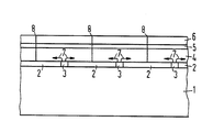
- the reference numeral 1 denotes a substrate body made of, for example, metallized glass or a flat silicon obtained by strip drawing. Then a highly doped, amorphous germanium layer 2 (a-Ge: P: H) with a phosphorus content of at least 1% by decomposing German (GeH.) And phosphine (PH,) in a low-pressure glow discharge reactor in a layer thickness of 0.2 deposited to 0.5 ⁇ m.
- a-Ge: P: H a highly doped, amorphous germanium layer 2 with a phosphorus content of at least 1% by decomposing German (GeH.) And phosphine (PH,) in a low-pressure glow discharge reactor in a layer thickness of 0.2 deposited to 0.5 ⁇ m.
- This germanium-phosphor layer 2 is crystallized with the aid of a pulsed or continuous wave laser of suitable wavelength (for germanium in the range of 1 ⁇ m) at certain points 3 (or lines), preferably with ⁇ 001> or ⁇ 111> orientation. This crystallization can also be achieved with an electron beam.
- ⁇ 001> and ⁇ 111> orientations are preferred crystal orientations for germanium.
- a subsequent gallium arsenide epitaxy carried out in a known manner and also suitable for the production of solar cells, for example from the organometallic compound Ga (CH,) and arsenic hydrogen or from arsenic hydrogen (AsH,) and gallium trichloride (GaCl 3 ) starts at the crystallization points (lines) 3.
- a deposition of gallium arsenide (4) on the amorphous areas of the germanium-phosphor layer 2 cannot take place due to the lack of lattice adaptation.
- the gallium arsenide of layer 4 starting from the predetermined crystallization points 3, the distances between which are preferably between 100 and 200 ⁇ m and the extent of which extends over approximately 5 ⁇ m, spreads laterally over the entire area in the direction of arrow 7 until the crystal fronts adjacent “epitaxial region” (3) meet.
- the growth areas are (001) or (111) areas.
- comm boundaries 8 are formed, which, however, are formed perpendicularly or approximately perpendicularly to the substrate surface 1 and thus have no appreciably harmful influence on the current collection of the solar cell.
- the grain boundaries 8 can be passivated by the hydrogen diffusing out of the amorphous germanium-phosphor layer 2 during epitaxy.
- the gallium arsenide is deposited at temperatures between 700 and 800 ° C, the gallium arsenide is deposited in crystalline form. At these temperatures, the amorphous germanium can crystallize, which favors gallium arsenide grain growth.
- the highly doped germanium-phosphor layer 2 forms the ohmic contact of the gallium arsenide solar cell with the conductive back contact (substrate 1).
- the crystallization structures (3) generated with the laser are selected in the range of 100 ⁇ m; this structure consequently also specifies the grain size. As is known from the literature, 10 ⁇ m grains are sufficient to achieve the high efficiency of monocrystalline gallium arsenide solar cells.
- a second gallium arsenide layer 5 of p-type with tin as dopant is deposited in a layer thickness of 0.2 to 1 ⁇ m in a known manner, and finally the arrangement is covered with a layer 6 consisting of a mixed aluminum-arsenic crystal.
- the layer 6, which has a layer thickness of 0.5 to .mu.m, is p-doped and serves as a window layer. It widens the band gap between the conduction and valence bands and prevents surface recombinations.
Landscapes
- Chemical & Material Sciences (AREA)
- Chemical Kinetics & Catalysis (AREA)
- General Chemical & Material Sciences (AREA)
- Engineering & Computer Science (AREA)
- Crystallography & Structural Chemistry (AREA)
- Materials Engineering (AREA)
- Metallurgy (AREA)
- Organic Chemistry (AREA)
- Photovoltaic Devices (AREA)
Applications Claiming Priority (2)
| Application Number | Priority Date | Filing Date | Title |
|---|---|---|---|
| DE3437233 | 1984-10-10 | ||
| DE3437233 | 1984-10-10 |
Publications (2)
| Publication Number | Publication Date |
|---|---|
| EP0180751A2 true EP0180751A2 (fr) | 1986-05-14 |
| EP0180751A3 EP0180751A3 (fr) | 1988-09-07 |
Family
ID=6247604
Family Applications (1)
| Application Number | Title | Priority Date | Filing Date |
|---|---|---|---|
| EP85112052A Withdrawn EP0180751A3 (fr) | 1984-10-10 | 1985-09-24 | Procédé de fabrication de cellules solaires à couche mince d'arséniure de gallium |
Country Status (3)
| Country | Link |
|---|---|
| US (1) | US4657603A (fr) |
| EP (1) | EP0180751A3 (fr) |
| JP (1) | JPS6195578A (fr) |
Cited By (13)
| Publication number | Priority date | Publication date | Assignee | Title |
|---|---|---|---|---|
| EP0244081A1 (fr) * | 1986-03-28 | 1987-11-04 | Canon Kabushiki Kaisha | Méthode de fabrication d'un cristal et article cristallin obtenu par cette méthode |
| EP0284433A3 (fr) * | 1987-03-27 | 1989-03-08 | Canon Kabushiki Kaisha | Articles cristallins et leur procédé de fabrication |
| EP0276961A3 (fr) * | 1987-01-26 | 1989-03-08 | Canon Kabushiki Kaisha | Batterie solaire et son procédé de fabrication |
| EP0289117A3 (en) * | 1987-03-02 | 1989-03-15 | Canon Kabushiki Kaisha | Method of forming crystals on a substrate |
| EP0284434A3 (fr) * | 1987-03-27 | 1989-03-22 | Canon Kabushiki Kaisha | Procédé de préparation de cristaux |
| EP0284441A3 (fr) * | 1987-03-26 | 1989-10-04 | Canon Kabushiki Kaisha | Produit cristallin composite du groupe II-VI et son procédé de fabrication |
| EP0288166A3 (en) * | 1987-03-26 | 1989-10-04 | Canon Kabushiki Kaisha | Process for selective formation of iii - v group compound film |
| EP0334110A3 (en) * | 1988-03-24 | 1990-03-14 | Siemens Aktiengesellschaft | Process for producing polycristalline layers with large crystals for thin film semiconductor devices, like solar cells |
| US5010033A (en) * | 1987-03-27 | 1991-04-23 | Canon Kabushiki Kaisha | Process for producing compound semiconductor using an amorphous nucleation site |
| EP0484922A1 (fr) * | 1990-11-07 | 1992-05-13 | Canon Kabushiki Kaisha | Dispositif semi-conducteur de composition III-V, dispositif d'impression et d'affichage utilisant celui-ci, et méthode de fabrication de celui-ci |
| US5254211A (en) * | 1987-03-27 | 1993-10-19 | Canon Kabushiki Kaisha | Method for forming crystals |
| DE19605245A1 (de) * | 1996-02-13 | 1997-08-14 | Siemens Ag | Verfahren zur Erzeugung von Kristallisationszentren auf der Oberfläche eines Substrats |
| US5846320A (en) * | 1986-03-31 | 1998-12-08 | Canon Kabushiki Kaisha | Method for forming crystal and crystal article obtained by said method |
Families Citing this family (31)
| Publication number | Priority date | Publication date | Assignee | Title |
|---|---|---|---|---|
| US4781766A (en) * | 1985-10-30 | 1988-11-01 | Astrosystems, Inc. | Fault tolerant thin-film photovoltaic cell and method |
| US4772564A (en) * | 1985-10-30 | 1988-09-20 | Astrosystems, Inc. | Fault tolerant thin-film photovoltaic cell fabrication process |
| JPS63108709A (ja) * | 1986-10-25 | 1988-05-13 | Toyota Central Res & Dev Lab Inc | 半導体装置およびその製造方法 |
| US5281283A (en) * | 1987-03-26 | 1994-01-25 | Canon Kabushiki Kaisha | Group III-V compound crystal article using selective epitaxial growth |
| CA1331950C (fr) * | 1987-03-26 | 1994-09-13 | Hiroyuki Tokunaga | Article cristallin de compose des groupes iii-v et procede pour sa production |
| US5304820A (en) * | 1987-03-27 | 1994-04-19 | Canon Kabushiki Kaisha | Process for producing compound semiconductor and semiconductor device using compound semiconductor obtained by same |
| US5364815A (en) * | 1987-03-27 | 1994-11-15 | Canon Kabushiki Kaisha | Crystal articles and method for forming the same |
| EP0297867B1 (fr) * | 1987-07-01 | 1993-10-06 | Nec Corporation | Procédé pour la croissance d'un cristal semi-conducteur d'un composé III-V sur un substrat de Si |
| AU623601B2 (en) * | 1987-08-08 | 1992-05-21 | Canon Kabushiki Kaisha | Method for growth of crystal |
| AU623861B2 (en) * | 1987-08-08 | 1992-05-28 | Canon Kabushiki Kaisha | Crystal article, method for producing the same and semiconductor device utilizing the same |
| US5363799A (en) * | 1987-08-08 | 1994-11-15 | Canon Kabushiki Kaisha | Method for growth of crystal |
| EP0307109A1 (fr) * | 1987-08-24 | 1989-03-15 | Canon Kabushiki Kaisha | Méthode pour former un cristal semi-conducteur et cristal semi-conducteur produit par cette méthode |
| AU615469B2 (en) * | 1987-08-24 | 1991-10-03 | Canon Kabushiki Kaisha | Crystal growth method |
| US4914053A (en) * | 1987-09-08 | 1990-04-03 | Texas Instruments Incorporated | Heteroepitaxial selective-area growth through insulator windows |
| US4826784A (en) * | 1987-11-13 | 1989-05-02 | Kopin Corporation | Selective OMCVD growth of compound semiconductor materials on silicon substrates |
| JPH01315127A (ja) * | 1988-03-18 | 1989-12-20 | Fujitsu Ltd | ガリウムヒ素層の形成方法 |
| US5238879A (en) * | 1988-03-24 | 1993-08-24 | Siemens Aktiengesellschaft | Method for the production of polycrystalline layers having granular crystalline structure for thin-film semiconductor components such as solar cells |
| US4935385A (en) * | 1988-07-22 | 1990-06-19 | Xerox Corporation | Method of forming intermediate buffer films with low plastic deformation threshold using lattice mismatched heteroepitaxy |
| US4994867A (en) * | 1988-07-22 | 1991-02-19 | Xerox Corporation | Intermediate buffer films with low plastic deformation threshold for lattice mismatched heteroepitaxy |
| US5190613A (en) * | 1988-10-02 | 1993-03-02 | Canon Kabushiki Kaisha | Method for forming crystals |
| JP2858434B2 (ja) * | 1989-03-31 | 1999-02-17 | キヤノン株式会社 | 結晶の形成方法および結晶物品 |
| US5094697A (en) * | 1989-06-16 | 1992-03-10 | Canon Kabushiki Kaisha | Photovoltaic device and method for producing the same |
| US5256594A (en) * | 1989-06-16 | 1993-10-26 | Intel Corporation | Masking technique for depositing gallium arsenide on silicon |
| JPH076960A (ja) * | 1993-06-16 | 1995-01-10 | Fuji Electric Co Ltd | 多結晶半導体薄膜の生成方法 |
| JP3322440B2 (ja) * | 1993-06-24 | 2002-09-09 | 三洋電機株式会社 | 薄膜多結晶シリコンの製造方法 |
| US5897331A (en) * | 1996-11-08 | 1999-04-27 | Midwest Research Institute | High efficiency low cost thin film silicon solar cell design and method for making |
| WO1999019546A1 (fr) | 1997-10-10 | 1999-04-22 | Cornell Research Foundation, Inc. | Procedes de croissance de couches heteroepitaxiales sans defaut |
| ES2232299B1 (es) * | 2003-11-04 | 2006-03-16 | Isofoton, S.A. | Procedimientos de ensamblaje de modulos fotovoltaicos de concentracion. |
| DE102005045096A1 (de) * | 2005-09-21 | 2007-03-29 | Institut für Physikalische Hochtechnologie e.V. | Dünnschichtsolarzelle und Verfahren zur Herstellung eines Halbleiterbauelements |
| JP4921205B2 (ja) * | 2007-02-27 | 2012-04-25 | 株式会社えいむ | メニューブック |
| CN102479848A (zh) * | 2010-11-24 | 2012-05-30 | 吉富新能源科技(上海)有限公司 | 三五族半导体的太阳能电池结构及其制作方法 |
Family Cites Families (3)
| Publication number | Priority date | Publication date | Assignee | Title |
|---|---|---|---|---|
| US4053350A (en) * | 1975-07-11 | 1977-10-11 | Rca Corporation | Methods of defining regions of crystalline material of the group iii-v compounds |
| US4370510A (en) * | 1980-09-26 | 1983-01-25 | California Institute Of Technology | Gallium arsenide single crystal solar cell structure and method of making |
| US4392297A (en) * | 1980-11-20 | 1983-07-12 | Spire Corporation | Process of making thin film high efficiency solar cells |
-
1985
- 1985-09-20 US US06/778,487 patent/US4657603A/en not_active Expired - Fee Related
- 1985-09-24 EP EP85112052A patent/EP0180751A3/fr not_active Withdrawn
- 1985-10-08 JP JP60222906A patent/JPS6195578A/ja active Pending
Non-Patent Citations (3)
| Title |
|---|
| APPLIED PHYSICS LETTERS, Band 41, Nr. 4, August 1982, Seiten 347-349, New York, US; B.-Y. TSAUR et al.: "Low-dislocation-density GaAs epilayers grown on Ge-coated Si substrates by means of lateral epitaxial overgrowth" * |
| EXTENDED ABSTRACTS, Band 84, Nr. 2, 1984, Seite 451, New Orleans, US; S.S. CHU et al.: "Gallium arsenide thin films on recrystallized germanium substrates" * |
| JOURNAL OF APPLIED PHYSICS, Band 48, Nr. 11, November 1977, Seiten 4848-4849, New York, US; S.S CHU et al.: "Gallium arsenide films on recrystallized germanium films" * |
Cited By (17)
| Publication number | Priority date | Publication date | Assignee | Title |
|---|---|---|---|---|
| EP0476713A3 (en) * | 1986-03-28 | 1992-08-05 | Canon Kabushiki Kaisha | Method for forming crystal and crystal article obtained by said method |
| US5853478A (en) * | 1986-03-28 | 1998-12-29 | Canon Kabushiki Kaisha | Method for forming crystal and crystal article obtained by said method |
| US5733369A (en) * | 1986-03-28 | 1998-03-31 | Canon Kabushiki Kaisha | Method for forming crystal |
| EP0244081A1 (fr) * | 1986-03-28 | 1987-11-04 | Canon Kabushiki Kaisha | Méthode de fabrication d'un cristal et article cristallin obtenu par cette méthode |
| US5846320A (en) * | 1986-03-31 | 1998-12-08 | Canon Kabushiki Kaisha | Method for forming crystal and crystal article obtained by said method |
| EP0276961A3 (fr) * | 1987-01-26 | 1989-03-08 | Canon Kabushiki Kaisha | Batterie solaire et son procédé de fabrication |
| EP0289117A3 (en) * | 1987-03-02 | 1989-03-15 | Canon Kabushiki Kaisha | Method of forming crystals on a substrate |
| EP0284441A3 (fr) * | 1987-03-26 | 1989-10-04 | Canon Kabushiki Kaisha | Produit cristallin composite du groupe II-VI et son procédé de fabrication |
| EP0288166A3 (en) * | 1987-03-26 | 1989-10-04 | Canon Kabushiki Kaisha | Process for selective formation of iii - v group compound film |
| US5010033A (en) * | 1987-03-27 | 1991-04-23 | Canon Kabushiki Kaisha | Process for producing compound semiconductor using an amorphous nucleation site |
| US5254211A (en) * | 1987-03-27 | 1993-10-19 | Canon Kabushiki Kaisha | Method for forming crystals |
| EP0284434A3 (fr) * | 1987-03-27 | 1989-03-22 | Canon Kabushiki Kaisha | Procédé de préparation de cristaux |
| EP0284433A3 (fr) * | 1987-03-27 | 1989-03-08 | Canon Kabushiki Kaisha | Articles cristallins et leur procédé de fabrication |
| EP0334110A3 (en) * | 1988-03-24 | 1990-03-14 | Siemens Aktiengesellschaft | Process for producing polycristalline layers with large crystals for thin film semiconductor devices, like solar cells |
| EP0484922A1 (fr) * | 1990-11-07 | 1992-05-13 | Canon Kabushiki Kaisha | Dispositif semi-conducteur de composition III-V, dispositif d'impression et d'affichage utilisant celui-ci, et méthode de fabrication de celui-ci |
| US5659184A (en) * | 1990-11-07 | 1997-08-19 | Canon Kabushiki Kaisha | III-V compound semiconductor device with a polycrystalline structure with minimum grain size of 0.6 μm and printer and display device utilizing the same |
| DE19605245A1 (de) * | 1996-02-13 | 1997-08-14 | Siemens Ag | Verfahren zur Erzeugung von Kristallisationszentren auf der Oberfläche eines Substrats |
Also Published As
| Publication number | Publication date |
|---|---|
| JPS6195578A (ja) | 1986-05-14 |
| EP0180751A3 (fr) | 1988-09-07 |
| US4657603A (en) | 1987-04-14 |
Similar Documents
| Publication | Publication Date | Title |
|---|---|---|
| EP0180751A2 (fr) | Procédé de fabrication de cellules solaires à couche mince d'arséniure de gallium | |
| DE4019209C2 (fr) | ||
| DE69229265T2 (de) | Verfahren zur herstellung und dotierung hochisolierender dünner schichten aus monokristallinem galliumnitrid | |
| DE4019219C2 (fr) | ||
| DE1933690C3 (de) | Verfahren zum Herstellen eines mindestens bereichsweise einkristallinen Films auf einem Substrat | |
| DE4138121C2 (de) | Verfahren zur Herstellung einer Solarzelle | |
| DE60101069T2 (de) | Siliziumkarbid und Verfahren zu seiner Herstellung | |
| DE3426338C2 (fr) | ||
| DE2943211C2 (de) | Amorphe Halbleiter auf Silizium- und/oder Germaniumbasis, ihre Verwendung und ihre Herstellung durch Glimmentladung | |
| DE3823249A1 (de) | Halbleitereinrichtung | |
| DE3105819A1 (de) | Amorphe filmsolarzelle | |
| DE3587853T2 (de) | Ein verfahren zur herstellung einer verbindungshalbleiterstruktur. | |
| DE3135393A1 (de) | Verfahren zum herstellen einer lichtempfindlichen amorphen legierung und diese enthaltendes bauelement | |
| DE3732418A1 (de) | Halbleiter-bauelement mit einem halbleiterbereich, in dem ein bandabstand kontinuierlich abgestuft ist | |
| DE2702860A1 (de) | Solarzelle und verfahren zu ihrer herstellung | |
| DE2231926B2 (de) | Verfahren zur Herstellung von Halbleitermaterial | |
| DE69411861T2 (de) | Photoelektrische Wandlervorrichtung aus polykrystallinem Silicon und Verfahren zur Herstellung | |
| DE2749607C3 (de) | Halbleiteranordnung und Verfahren zu deren Herstellung | |
| DE2844070A1 (de) | Amorpher halbleiter | |
| DE19634617A1 (de) | Solarzelle | |
| DE3850582T2 (de) | Gallium-Nitrid Halbleiter-Lumisneszenzdiode sowie Verfahren zu deren Herstellung. | |
| EP0541033A2 (fr) | Procédé de fabrication de cellules solaires à couche minces en silicium polycristallin | |
| DE4039390A1 (de) | Solarbatterie und verfahren zu deren hertellung | |
| DE69218022T2 (de) | Lichtemittierende Vorrichtung unter Verwendung von polykristallinem Halbleitermaterial und Herstellungsverfahren dafür | |
| DE69026767T2 (de) | Elektrode mit ohmschem Kontakt für Halbleiterdiamanten |
Legal Events
| Date | Code | Title | Description |
|---|---|---|---|
| PUAI | Public reference made under article 153(3) epc to a published international application that has entered the european phase |
Free format text: ORIGINAL CODE: 0009012 |
|
| AK | Designated contracting states |
Kind code of ref document: A2 Designated state(s): DE FR GB IT |
|
| PUAL | Search report despatched |
Free format text: ORIGINAL CODE: 0009013 |
|
| AK | Designated contracting states |
Kind code of ref document: A3 Designated state(s): DE FR GB IT |
|
| STAA | Information on the status of an ep patent application or granted ep patent |
Free format text: STATUS: THE APPLICATION IS DEEMED TO BE WITHDRAWN |
|
| 18D | Application deemed to be withdrawn |
Effective date: 19890331 |
|
| RIN1 | Information on inventor provided before grant (corrected) |
Inventor name: KRUEHLER, WOLFGANG, DR. Inventor name: GRABMAIER, JOSEF, DR. |