EP0180929A2 - Elektrooptische Schreibeinrichtung - Google Patents
Elektrooptische Schreibeinrichtung Download PDFInfo
- Publication number
- EP0180929A2 EP0180929A2 EP85113921A EP85113921A EP0180929A2 EP 0180929 A2 EP0180929 A2 EP 0180929A2 EP 85113921 A EP85113921 A EP 85113921A EP 85113921 A EP85113921 A EP 85113921A EP 0180929 A2 EP0180929 A2 EP 0180929A2
- Authority
- EP
- European Patent Office
- Prior art keywords
- optical
- writing device
- electro
- line
- electrodes
- Prior art date
- Legal status (The legal status is an assumption and is not a legal conclusion. Google has not performed a legal analysis and makes no representation as to the accuracy of the status listed.)
- Granted
Links
Images




Classifications
-
- B—PERFORMING OPERATIONS; TRANSPORTING
- B41—PRINTING; LINING MACHINES; TYPEWRITERS; STAMPS
- B41J—TYPEWRITERS; SELECTIVE PRINTING MECHANISMS, i.e. MECHANISMS PRINTING OTHERWISE THAN FROM A FORME; CORRECTION OF TYPOGRAPHICAL ERRORS
- B41J2/00—Typewriters or selective printing mechanisms characterised by the printing or marking process for which they are designed
- B41J2/435—Typewriters or selective printing mechanisms characterised by the printing or marking process for which they are designed characterised by selective application of radiation to a printing material or impression-transfer material
- B41J2/465—Typewriters or selective printing mechanisms characterised by the printing or marking process for which they are designed characterised by selective application of radiation to a printing material or impression-transfer material using masks, e.g. light-switching masks
-
- G—PHYSICS
- G02—OPTICS
- G02F—OPTICAL DEVICES OR ARRANGEMENTS FOR THE CONTROL OF LIGHT BY MODIFICATION OF THE OPTICAL PROPERTIES OF THE MEDIA OF THE ELEMENTS INVOLVED THEREIN; NON-LINEAR OPTICS; FREQUENCY-CHANGING OF LIGHT; OPTICAL LOGIC ELEMENTS; OPTICAL ANALOGUE/DIGITAL CONVERTERS
- G02F1/00—Devices or arrangements for the control of the intensity, colour, phase, polarisation or direction of light arriving from an independent light source, e.g. switching, gating or modulating; Non-linear optics
- G02F1/01—Devices or arrangements for the control of the intensity, colour, phase, polarisation or direction of light arriving from an independent light source, e.g. switching, gating or modulating; Non-linear optics for the control of the intensity, phase, polarisation or colour
- G02F1/03—Devices or arrangements for the control of the intensity, colour, phase, polarisation or direction of light arriving from an independent light source, e.g. switching, gating or modulating; Non-linear optics for the control of the intensity, phase, polarisation or colour based on ceramics or electro-optical crystals, e.g. exhibiting Pockels effect or Kerr effect
- G02F1/055—Devices or arrangements for the control of the intensity, colour, phase, polarisation or direction of light arriving from an independent light source, e.g. switching, gating or modulating; Non-linear optics for the control of the intensity, phase, polarisation or colour based on ceramics or electro-optical crystals, e.g. exhibiting Pockels effect or Kerr effect the active material being a ceramic
- G02F1/0551—Constructional details
Definitions
- the invention relates to an electro-optical writing device for line-by-line recording of image information, an electrically controllable optical component having pixel elements being provided, from which point-by-point light strikes a recording medium along the length of a recording line.
- Such electro-optical writing devices are known (DE-OS 3 1 13293). They are installed as an essential functional unit in optical printers.
- They consist of an electro-optical switch, a light source and a recording medium.
- the relevant structural unit is the electro-optical switch 11, the function of which is based on an optically active layer 14.
- the layer consists of an optically active ceramic, e.g. a PLZT ceramic (ceramic consisting of the chemical elements lead, lanthanum, zirconium and titanium) and is switched from the optically isotropic to the optically anisotropic state by applying an electrical field.
- Optically anisotropic means that the refractive index is anisotropic, which is also referred to as optically birefringent. If linearly polarized light now passes through the birefringent ceramic 14, its polarization plane rotates.
- this unit By mounting a polarizer 15 in front and an analyzer 16 behind the birefringent ceramic, this unit can be used as an electro-optical switch 11.
- a pixel is controlled by applying a voltage to the pair of electrodes attached to the optical ceramic. The resulting electrical field leads the ceramic from the optically isotropic to the optically birefringent state. The electro-optical switch becomes transparent for this pixel
- One problem is the creation of the Elsktric field. Since in the optical printer the exposure of the recording medium is generally carried out line by line, the switch must also be constructed as a line. On the other hand, a high resolution is also required, which leads to a correspondingly dense arrangement of the electrodes via which the electric field is applied. These electrodes are applied using thin or thick-film technology. In the conventional technology and the known optically active material, a minimum distance between two adjacent electrodes and a minimum electrode width are required in order to ensure the functionality. The known writing device specified above enables a resolution of eight dots per mm.
- the object of the invention is to provide a writing device which requires a smaller number of drivers.
- the electrode structure enables a number of pixels which is twice as large as an associated number of driver stages.
- the remaining driver stages with cables have more space available and can therefore be dimensioned larger, which increases the functional reliability of each individual stage. Halving the driver stages further doubles the functional reliability of the electro-optical writing device.
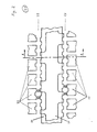
- the electrode structure 21 of a writing device according to the invention can be seen from FIG. 2.
- a recording line is exposed by the two optical lines 22 and 23.
- Four successive points a to d are controlled by the electrodes 24, 25 and the center electrodes 26 and 27.
- the electrodes 24 control the central electrodes 26 and 27, for example, the points a and c, the electrodes 25 together with the central electrodes 26 and 27, the point b lying on the record carrier between the points a and c and the point d following the point c.
- Point a is controlled when there is voltage between electrodes 24 and 26, the other points are controlled accordingly.
- FIG. 3 shows the section through the electrode structure including the optically birefringent substrate 32.
- the electrodes 24 and 25 and the center electrode 26 are applied directly to the substrate 32.
- an insulating layer 33 covers the electrodes that have already been applied and almost the entire surface of the substrate. Only small windows 34 remain free at the locations through which the upper center electrode 27 is in direct contact with the substrate 32.
- the primary function of the insulating layer 33 is to electrically separate the electrodes 26 and 27.
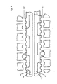
- the two center electrodes are divided into four center electrodes 41, 42 , 43, 44 .
- the electronic separation of the two optical lines enables the resolution to be changed from, for example, eight points per mm to four points per mm, which results in a shorter data transmission time in the case of digital data transmission with appropriate control.
- points a and b as well as c and d are controlled together and each represent only one point.
- an optical writing device With an optical writing device according to FIG. 5, less sensitive recording media can also be written without increasing the exposure time or the light intensity.
- the arrangement is chosen so that the two optical lines are shifted by one pixel relative to one another in the above-mentioned exemplary embodiments.
- the originally four points a, b, c and d form here only two points a and b, which are however double. This doubles the effective exposure time without increasing the printing time.
- the electrode ends 65 to 68 determining the pixel are referred to here as electrode tips.
- the electrode tips 65 of the electrodes 6 1 and 6 4 are shifted by a length s with respect to the electrode tips 66 of the electrodes 62 and 63.
- the corresponding electrode tips 67 and 68 of the electrodes 24 and 25 are also shifted by the length s, which again leads to a uniform electrode tip spacing 69.
- the optical line 22 is activated accordingly. This has the consequence that all the pixels of a recording line are at one level again.
- the advantage of this arrangement lies in the application of the electrodes 62 and 63, which are applied to the insulating layer 33 (see FIG. 3) and through the window 34 directly to the substrate 32 without touching the electrodes 61 and 63. This arrangement leaves enough space at the critical points and thus simplifies the manufacture of the electro-optical writing device.
Landscapes
- Physics & Mathematics (AREA)
- Chemical & Material Sciences (AREA)
- Engineering & Computer Science (AREA)
- Ceramic Engineering (AREA)
- Nonlinear Science (AREA)
- Crystallography & Structural Chemistry (AREA)
- General Physics & Mathematics (AREA)
- Optics & Photonics (AREA)
- Printers Or Recording Devices Using Electromagnetic And Radiation Means (AREA)
- Liquid Crystal (AREA)
- Devices For Indicating Variable Information By Combining Individual Elements (AREA)
- Electrochromic Elements, Electrophoresis, Or Variable Reflection Or Absorption Elements (AREA)
Abstract
Description
- Die Erfindung betrifft eine elektrooptische Schreibeinrichtung zur zeilenweise Aufzeichnung von Bildinformationen, wobei ein elektrisch steuerbares optisches Bauteil mit Bildpunktelementen vorhanden ist, von dem aus punktweise Licht entlang der Länge einer Aufzeichnungszeile auf einen Aufzeichnungsträger fällt.
- Derartige elektrooptische Schreibeinrichtungen sind bekannt (DE-OS 3113293). Sie sind als eine wesentliche Funktionseinheit in optischen Druckern eingebaut.
- Sie bestehen aus einem elektrooptischen Schalter, einer Lichtquelle und einem Aufzeichnungsträger.
- Die Wirkung einer elektrooptischen Schreibeinrichtung 10 wird nun anhand von Fig. 1 erläutert. Die relevante Baueinheit stellt der elektrooptische Schalter 11 dar, dessen Funktion auf einer optisch aktiven Schicht 14 beruht. Die Schicht besteht aus einer optischen aktiven Keramik, Z.B. einer PLZT-Keramik (Keramik, die aus den chemischen Elementen Blei, Lanthan, Zirkon und Titan besteht) und wird durch Anlegen eines elektrischen Feldes vom optisch isotropen in den optisch anisotropen Zustand versetzt. Optisch anisotrop bedeutet, der Brechungsindex ist anisotrop, was auch als optisch doppelbrechend bezeichnet wird. Tritt nun linear polarisiertes Licht durch die doppelbrechende Keramik 14, dreht sich seine Polarisationsebene. Durch die Montage eines Polarisators 15 vor und eines Analysators 16 hinter der doppelbrechenden Keramik kann diese Einheit als elektrooptischer Schalter 11 verwendet werden. Ein Bildpunkt wird dabei angesteuert, indem dem auf der optischen Keramik angebrachten Elektrodenpaar eine Spannung angelegt wird. Das somit entstehende elektrische Feld führt die Keramik vom optisch isotropen in den optisch doppelbrechenden Zustand über. Der elektrooptische Schalter wird für diesen Bildpunkt transparent
- Ein Problem liegt im Anlegen des elsktrischen Feldes. Da beim optischen Drucker in der Regel die Belichtung des Aufzeichnungsträgers zeilenweise erfolgt, muß der Schalter auch als Zeile aufgebaut sein. Andererseits wird auch eine hohe Auflösung gefordert, was zu einer entsprechend dichten Anordnung der Elektroden führt, über die das elektrische Feld angelegt wird. Diese Elektroden werden in Dünn- oder auch Dickschichttechnik aufgebracht Bei der herkömmlichen Technik und dem bekannten optisch aktiven Material sind ein Minimalabstand zwischen zwei benachbarten Elektroden und eine minimale Elektrodenbreite erforderlich, um die Funktionsfähigkeit zu gewährleisten. Die oben angegebene bekannte Schreibeinrichtung ermöglicht eine Auflösung von acht Punkten pro mm.
- Bei dieser Anordnung wird für jedes Elektrodenpaar ein Treiber zum Ansteuern benötigt und diese führt zu einer entsprechend hohen Anzahl von Transistoren. Da mit der Anzahl der Bauteile auch die Ausfallsrate steigt, sind die elektrooptischen Schalter mit hoher Auflösung störanfällig. Ein einziger nicht funktionsfähiger Bildpunkt der Schreibeinrichtung wirkt sich dabei derart störend aus, daß die Schreibeinrichtung ausgewechselt werden muß.
- Die Aufgabe der Erfindung besteht darin, eine Schreibeinrichtung zu schaffen, die eine geringere Anzahl von Treibern benötigt.
- Diese Aufgabe wird bei einer Schreibeinrichtung der eingangs genannten Art dadurch gelöst, daß die elektrooptische Schreibeinrichtung eine Elektrodenstruktur aufweist, die das Ansteuern von N Bildpunkten mit N/2 Treiberstufen benötigt.
- Die Unteransprüche zeigen vorteilhafte Ausgestaltungen des Erfindungsgegenstandes auf.
- Die durch die Erfindung erzielten Vorteile bestehen insbesondere darin, daß die Elektrodenstruktur eine Anzahl von Bildpunkten ermöglicht, die doppelt so groß ist, wie eine dazugehörige Anzahl von Treiberstufen. Als Konsequenz daraus steht den verbleibenden Treiberstufen mit Leitungen mehr Platz zur Verfügung und sie können dadurch größer dimensioniert werden, was die Funktionssicherheit jeder einzelnen Stufe vergrößert. Die Halbierung der Treiberstufen verdoppelt die Funktionssicherheit der elektrooptischen Schreibeinrichtung noch zusätzlich.
- Die Erfindung wird nachstehend anhand von Ausführungsbeispielen unter Bezugnahme auf die Zeichnungen näher erläutert. Es zeigen:
- Fig. 1 den prinzipiellen Aufbau einer elektrooptischen Schreibeinrichtung;
- Fig. 2 eine Schreibeinrichtung gemäß der Erfindung, in einer Draufsicht, aus der die Elektrodenstruktur ersichtlich ist
- Fig. 3 die Schreibeinrichtung nach Fig. 1, in einem Teilschnitt
- Fig. 4 eine Draufsicht einer Schreibeinrichtung mit einer anderen Elektrodenstruktur;
- Fig. 5 eine Schreibeinrichtung mit einer weiteren Elektrodenstruktur, in der Draufsicht, und
- Fig. 6 eine Schreibeinrichtung mit einer vierten Elektrodenstruktur, in der Draufsicht.
- Die Elektrodenstruktur 21 einer erfindungsgemäßen Schreibeinrichtung ist aus Fig. 2 ersichtlich. Eine Aufzeichnungszeile wird in diesem Fall durch die beiden optischen Zeilen 22 und 23 belichtet. Dabei werden vier aufeinanderfolgende Punkte a bis d von den Elektroden 24, 25 und den Mittelelektroden 26 und 27 angesteuert. Die Elektroden 24 steuern dabei mit den Mittelelektroden 26 und 27 beispielsweise die Punkte a und c, die Elektroden 25 zusammen mit den Mittelelektroden 26 und 27, den auf dem Aufzeichnungsträger zwischen den Punkten a und c liegenden Punkt b und den Punkt c nachfolgenden Punkt d. Punkt a wird gesteuert, wenn Spannung zwischen den Elektroden 24 und 26 anliegt, die anderen Punkte werden entsprechend gesteuert.
- In Fig. 3 ist der Schnitt durch die Elektrodenstruktur einschließlich des optisch doppelbrechenden Substrats 32 dargestellt. Die Elektroden 24 und 25 und die Mittelelektrode 26 sind direkt auf das Substrat 32 aufgebracht. Als zweite Schicht bedeckt eine Isolierschicht 33 die schon aufgebrachten Elektroden und fast die gesamte Fläche des Substrats. Es bleiben nur kleine Fenster 34 an den Stellen frei, durch die die obere Mittelelektrode 27 direkten Kontakt zum Substrat 32 hat. Die Isolierschicht 33 hat primär die Aufgabe, die Elektroden 26 und 27 elektrisch zu trennen. Die Isolierschicht 33 wird in ihrer Dicke so dimensioniert, daß sie an den Bildpunkten z.B. a bis d als λ /4-Schicht (λ = relevante Wellenlänge des Lichtes der Lichtquelle 12) und somit als Antireflexionsschicht wirkt. Bei herkömmlichen Anordnungen mußte diese Schicht zusätzlich aufgebracht werden.
- Bei dem aus Fig. 4 ersichtlichen Ausführungsbeispiel sind die beiden Mittelelektroden in vier Mittelelektroden 41, 42, 43, 44 aufgeteilt. Dies bedeutet eine vollkommene elektrische Trennung der beiden optischen Zeilen 22 und 23, die es ermöglicht einen Schlupf beim Transport des Aufzeichnungsträgers 13, oder Gleichlaufschwankungen eines Trommelplotters zu korrigieren. Weiter ermöglicht die elektronische Trennung der beiden optischen Zeilen eine Veränderung der Auflösung von beispielsweise acht Punkten pro mm auf vier Punkte pro mm, was bei einer digitalen Datenübermittlung mit entsprechender Ansteuerung eine kürzere Datenübertragungszeit zur Folge hat. Die Punkte a und b sowie c und d werden in diesem Fall gemeinsam angesteuert und stellen jeweils auch nur einen Punkt dar.
- Mit einer optischen Schreibeinrichtung nach Fig. 5 können auch weniger empfindliche Aufzeichnungsträger beschrieben werden, ohne die Belichtungszeit oder die Lichtintensität zu erhöhen. Die Anordnung ist so gewählt, daß die beiden optischen Zeilen gegenüber den in den obengenannten Ausführungsbeispielen um einen Bildpunkt zueinander verschoben sind. Die ursprünglich vier Punkte a, b, c und d bilden hier nur noch zwei Punkte a und b, die aber doppelt vorliegen. Die effektive Belichtungszeit wird hierdurch verdoppelt, ohne die Druckzeit zu erhöhen. Bei der in Fig. 6 dargestellten optischen Schreibeinrichtung liegen vier Mitteielektroden 61, 62, 63 und 64 vor. Die den Bildpunkt bestimmenden Elektrodenenden 65 bis 68 werden hier als Elektrodenspitzen bezeichnet. Dabei sind die Elektrodenspitzen 65 der Elektroden 61 und 64 gegenüber den Elektrodenspitzen 66 der Elektroden 62 und 63 um eine Länge s verschoben. Die entsprechenden Elektrodenspitzen 67 und 68 der Elektroden 24 und 25 sind ebenfalls um die Länge s verschoben, was wieder zu einem einheitlichen Elektrodenspitzenabstand 69 führt. Zur Belichtung der optischen Zeile 23 wird die Elektrode 63 nun um die Zeit t früher als die Elektrode 64 angesteuert, mit t = slv, wobei v die Vorschubgeschwindigkeit des Aufzeichnungsträgers ist. Entsprechend erfolgt die Ansteuerung der optischen Zeile 22. Das hat zur Folge, daß wieder alle Bildpunkte einer Aufzeichnungszeile auf einer Höhe liegen. Der Vorteil dieser Anordnung liegt in der Aufbringung der Elektroden 62 und 63, die auf die Isolierschicht 33 (siehe Fig. 3) und durch das Fenster 34 direkt auf das Substrat 32 aufgebracht werden, ohne die Elektroden 61 und 63 zu berühren. Diese Anordnung läßt an den kritischen Stellen genügend Platz und vereinfacht somit die Herstellung der elektrooptischen Schreibeinrichtung.
Claims (6)
Applications Claiming Priority (2)
| Application Number | Priority Date | Filing Date | Title |
|---|---|---|---|
| DE3440406 | 1984-11-06 | ||
| DE19843440406 DE3440406A1 (de) | 1984-11-06 | 1984-11-06 | Elektrooptische schreibeinrichtung |
Publications (3)
| Publication Number | Publication Date |
|---|---|
| EP0180929A2 true EP0180929A2 (de) | 1986-05-14 |
| EP0180929A3 EP0180929A3 (en) | 1987-11-04 |
| EP0180929B1 EP0180929B1 (de) | 1991-05-29 |
Family
ID=6249547
Family Applications (1)
| Application Number | Title | Priority Date | Filing Date |
|---|---|---|---|
| EP85113921A Expired - Lifetime EP0180929B1 (de) | 1984-11-06 | 1985-10-31 | Elektrooptische Schreibeinrichtung |
Country Status (4)
| Country | Link |
|---|---|
| US (1) | US4658271A (de) |
| EP (1) | EP0180929B1 (de) |
| JP (1) | JPS61117518A (de) |
| DE (2) | DE3440406A1 (de) |
Families Citing this family (2)
| Publication number | Priority date | Publication date | Assignee | Title |
|---|---|---|---|---|
| DE3617249A1 (de) * | 1986-05-22 | 1987-11-26 | Standard Elektrik Lorenz Ag | Elektrodenstruktur fuer einen druckkopf |
| DE4214036A1 (de) * | 1992-04-29 | 1993-11-04 | Abb Patent Gmbh | Vorrichtung zum empfang von fokussierter lichtstrahlung |
Family Cites Families (7)
| Publication number | Priority date | Publication date | Assignee | Title |
|---|---|---|---|---|
| JPS54152998A (en) * | 1978-05-24 | 1979-12-01 | Seiko Epson Corp | Matrix electrode structure |
| FR2483088A1 (fr) * | 1980-05-20 | 1981-11-27 | Commissariat Energie Atomique | Procede de fabrication de portes optiques et de leur circuit de commande |
| US4370030A (en) * | 1980-05-27 | 1983-01-25 | Xerox Corporation | Extended resolution light deflector using surface acoustic waves |
| US4560994A (en) * | 1981-10-08 | 1985-12-24 | Xerox Corporation | Two dimensional electro-optic modulator for printing |
| JPS5882222A (ja) * | 1981-11-11 | 1983-05-17 | Matsushita Electric Ind Co Ltd | 光シヤツタ−素子 |
| US4458989A (en) * | 1982-06-16 | 1984-07-10 | Eastman Kodak Company | Electro-optic addressing apparatus and novel modulator configurations for use therein |
| JP3478670B2 (ja) * | 1996-06-18 | 2003-12-15 | キヤノン株式会社 | 印刷制御装置と印刷装置及びそれらの方法と印刷システム |
-
1984
- 1984-11-06 DE DE19843440406 patent/DE3440406A1/de not_active Withdrawn
-
1985
- 1985-10-31 DE DE8585113921T patent/DE3583001D1/de not_active Expired - Lifetime
- 1985-10-31 EP EP85113921A patent/EP0180929B1/de not_active Expired - Lifetime
- 1985-11-06 US US06/796,040 patent/US4658271A/en not_active Expired - Fee Related
- 1985-11-06 JP JP60247290A patent/JPS61117518A/ja active Granted
Also Published As
| Publication number | Publication date |
|---|---|
| EP0180929B1 (de) | 1991-05-29 |
| DE3440406A1 (de) | 1986-05-07 |
| JPS61117518A (ja) | 1986-06-04 |
| EP0180929A3 (en) | 1987-11-04 |
| DE3583001D1 (de) | 1991-07-04 |
| US4658271A (en) | 1987-04-14 |
| JPH0263215B2 (de) | 1990-12-27 |
Similar Documents
| Publication | Publication Date | Title |
|---|---|---|
| DE3587443T2 (de) | Flüssigkristall-Anzeigebaustein. | |
| EP0025957B1 (de) | Optische Vorrichtung zum berührungslosen Schreiben, insbesondere zur Faksimilewiedergabe von Bildern und Text | |
| EP0078339B1 (de) | Tastkopfanordnung für Leiterzugüberprüfung mit mindestens einem, eine Vielzahl von federnden Kontakten aufweisenden Tastkopf | |
| DE2449543C3 (de) | Verfahren zum Treiben einer Flüssigkristall-Matrixanzeigeeinheit | |
| DE69111906T2 (de) | Verfahren zur Herstellung von Matrixen von MIM-Anordnungen und solche Matrixen enthaltende Anzeigevorrichtungen. | |
| DE10139095B4 (de) | Flüssigkristallanzeige | |
| DE102017205654A1 (de) | Array-Substrat, Anzeigetafel und Steuerungsverfahren | |
| DE1946815C3 (de) | Anordnung zur elektrostatischen Aufzeichnung | |
| DE3033520C2 (de) | Lese- und Aufzeichnungsvorrichtung | |
| DE2261786C3 (de) | ||
| DE4005494C2 (de) | Halbleiter-Vorrichtung sowie Bildlesegerät mit dieser Halbleitervorrichtung mit optimierten elektrischen Eigenschaften | |
| DE2301335C3 (de) | Faksimile-Verfahren mit abwechselnder Verwendung einer Endstation als Empfänger oder Sender | |
| DE3841601B4 (de) | Lichtverschlußvorrichtung | |
| DE3018452C2 (de) | Faksimile-Schreibeinrichtung | |
| DE69009033T2 (de) | Abtaster. | |
| DE2557254A1 (de) | Faksimile-schreibeinrichtung | |
| DE69430895T2 (de) | Anzeigevorrichtung mit Flüssigkristallen | |
| EP0180929A2 (de) | Elektrooptische Schreibeinrichtung | |
| DE69127588T2 (de) | Optisches Modulationselement und sein Herstellungsverfahren | |
| DE2712619A1 (de) | Schaltsystem, insbesondere eltktrographisches schreibsystem | |
| DE2110481B2 (de) | Thermodruckkopf | |
| DE3214584C2 (de) | Elektrooptische Vorrichtung | |
| DE68908988T2 (de) | Elektrooptische Zelle. | |
| DE4243653B4 (de) | Elektrodenstruktur eines Flüssigkristallanzeigefeldes | |
| DE3873651T2 (de) | Ladungsniederschlagssteuerung in einem elektrographischen duennschicht-druckkopf. |
Legal Events
| Date | Code | Title | Description |
|---|---|---|---|
| PUAI | Public reference made under article 153(3) epc to a published international application that has entered the european phase |
Free format text: ORIGINAL CODE: 0009012 |
|
| AK | Designated contracting states |
Kind code of ref document: A2 Designated state(s): DE FR GB IT NL |
|
| RAP1 | Party data changed (applicant data changed or rights of an application transferred) |
Owner name: STANDARD ELEKTRIK LORENZ AKTIENGESELLSCHAFT Owner name: ALCATEL N.V. |
|
| PUAL | Search report despatched |
Free format text: ORIGINAL CODE: 0009013 |
|
| AK | Designated contracting states |
Kind code of ref document: A3 Designated state(s): DE FR GB IT NL |
|
| RAP3 | Party data changed (applicant data changed or rights of an application transferred) |
Owner name: STANDARD ELEKTRIK LORENZ AKTIENGESELLSCHAFT Owner name: ALCATEL N.V. |
|
| 17P | Request for examination filed |
Effective date: 19880427 |
|
| 17Q | First examination report despatched |
Effective date: 19890714 |
|
| ITF | It: translation for a ep patent filed | ||
| GRAA | (expected) grant |
Free format text: ORIGINAL CODE: 0009210 |
|
| AK | Designated contracting states |
Kind code of ref document: B1 Designated state(s): DE FR GB IT NL |
|
| GBT | Gb: translation of ep patent filed (gb section 77(6)(a)/1977) | ||
| REF | Corresponds to: |
Ref document number: 3583001 Country of ref document: DE Date of ref document: 19910704 |
|
| ET | Fr: translation filed | ||
| PLBE | No opposition filed within time limit |
Free format text: ORIGINAL CODE: 0009261 |
|
| STAA | Information on the status of an ep patent application or granted ep patent |
Free format text: STATUS: NO OPPOSITION FILED WITHIN TIME LIMIT |
|
| 26N | No opposition filed | ||
| PGFP | Annual fee paid to national office [announced via postgrant information from national office to epo] |
Ref country code: DE Payment date: 19921212 Year of fee payment: 8 |
|
| PGFP | Annual fee paid to national office [announced via postgrant information from national office to epo] |
Ref country code: FR Payment date: 19930930 Year of fee payment: 9 |
|
| PGFP | Annual fee paid to national office [announced via postgrant information from national office to epo] |
Ref country code: GB Payment date: 19931021 Year of fee payment: 9 |
|
| PGFP | Annual fee paid to national office [announced via postgrant information from national office to epo] |
Ref country code: NL Payment date: 19931031 Year of fee payment: 9 |
|
| PG25 | Lapsed in a contracting state [announced via postgrant information from national office to epo] |
Ref country code: DE Effective date: 19940701 |
|
| PG25 | Lapsed in a contracting state [announced via postgrant information from national office to epo] |
Ref country code: GB Effective date: 19941031 |
|
| PG25 | Lapsed in a contracting state [announced via postgrant information from national office to epo] |
Ref country code: NL Effective date: 19950501 |
|
| NLV4 | Nl: lapsed or anulled due to non-payment of the annual fee | ||
| GBPC | Gb: european patent ceased through non-payment of renewal fee |
Effective date: 19941031 |
|
| PG25 | Lapsed in a contracting state [announced via postgrant information from national office to epo] |
Ref country code: FR Effective date: 19950630 |
|
| REG | Reference to a national code |
Ref country code: FR Ref legal event code: ST |