EP0181030B1 - Dispositif pour surveiller un convertisseur de code CMI - Google Patents
Dispositif pour surveiller un convertisseur de code CMI Download PDFInfo
- Publication number
- EP0181030B1 EP0181030B1 EP85201746A EP85201746A EP0181030B1 EP 0181030 B1 EP0181030 B1 EP 0181030B1 EP 85201746 A EP85201746 A EP 85201746A EP 85201746 A EP85201746 A EP 85201746A EP 0181030 B1 EP0181030 B1 EP 0181030B1
- Authority
- EP
- European Patent Office
- Prior art keywords
- signal
- cmi
- input
- output
- divider
- Prior art date
- Legal status (The legal status is an assumption and is not a legal conclusion. Google has not performed a legal analysis and makes no representation as to the accuracy of the status listed.)
- Expired
Links
- 230000005540 biological transmission Effects 0.000 claims description 4
- 238000010586 diagram Methods 0.000 description 6
- 238000006243 chemical reaction Methods 0.000 description 4
- 230000003111 delayed effect Effects 0.000 description 2
- 239000002131 composite material Substances 0.000 description 1
- 238000010276 construction Methods 0.000 description 1
- 230000002950 deficient Effects 0.000 description 1
- 238000000034 method Methods 0.000 description 1
Images

Classifications
-
- H—ELECTRICITY
- H04—ELECTRIC COMMUNICATION TECHNIQUE
- H04L—TRANSMISSION OF DIGITAL INFORMATION, e.g. TELEGRAPHIC COMMUNICATION
- H04L1/00—Arrangements for detecting or preventing errors in the information received
- H04L1/24—Testing correct operation
- H04L1/245—Testing correct operation by using the properties of transmission codes
- H04L1/246—Testing correct operation by using the properties of transmission codes two-level transmission codes, e.g. binary
-
- H—ELECTRICITY
- H04—ELECTRIC COMMUNICATION TECHNIQUE
- H04L—TRANSMISSION OF DIGITAL INFORMATION, e.g. TELEGRAPHIC COMMUNICATION
- H04L25/00—Baseband systems
- H04L25/38—Synchronous or start-stop systems, e.g. for Baudot code
- H04L25/40—Transmitting circuits; Receiving circuits
- H04L25/49—Transmitting circuits; Receiving circuits using code conversion at the transmitter; using predistortion; using insertion of idle bits for obtaining a desired frequency spectrum; using three or more amplitude levels ; Baseband coding techniques specific to data transmission systems
- H04L25/4906—Transmitting circuits; Receiving circuits using code conversion at the transmitter; using predistortion; using insertion of idle bits for obtaining a desired frequency spectrum; using three or more amplitude levels ; Baseband coding techniques specific to data transmission systems using binary codes
- H04L25/4908—Transmitting circuits; Receiving circuits using code conversion at the transmitter; using predistortion; using insertion of idle bits for obtaining a desired frequency spectrum; using three or more amplitude levels ; Baseband coding techniques specific to data transmission systems using binary codes using mBnB codes
- H04L25/491—Transmitting circuits; Receiving circuits using code conversion at the transmitter; using predistortion; using insertion of idle bits for obtaining a desired frequency spectrum; using three or more amplitude levels ; Baseband coding techniques specific to data transmission systems using binary codes using mBnB codes using 1B2B codes
- H04L25/4912—Transmitting circuits; Receiving circuits using code conversion at the transmitter; using predistortion; using insertion of idle bits for obtaining a desired frequency spectrum; using three or more amplitude levels ; Baseband coding techniques specific to data transmission systems using binary codes using mBnB codes using 1B2B codes using CMI or 2-HDB-3 code
Definitions
- the invention relates to an arrangement for supervising a CMI-code converter in a PCM-multiplex transmission system, in which a binary signal is converted into a CMI-signal or vice versa, the code converter having a first terminal for the CMI-signal and a second terminal for the binary signal.
- a digital signal is applied at the transmitting side to a CMI-encoding unit in which the digital signal is converted into the CMI-code format (coded mark inversion) recommended for the bit rate.
- the CMI-code is-a two- level code in which a logic 0 bit is encoded such that each of the two levels is present during half a bit time interval, first one level and thereafter the other level.
- a logic 1 bit is encoded by one of the two levels during an entire bit period interval and in such a manner that the level alternates for sequential logic 1 bits.
- the digital path comprises a CMI-decoder unit in which after equalization and recovering with the aid of the recovered system clock the received CMI-encoded signal is converted into the normal binary code.
- the original, composite digital signal is then available at the output of the CMI-decoding unit with the nominal bit rate and the original system clock.
- a supervision circuit of said type is to have any practical sense, then the restriction holds that the complexity of the supervision circuit must be low compared with the circuit it supervises. This excludes, for example, a bit-by-bit comparison. Also operating with twice the clock frequency of the input signal for transmitting the two levels in one bit period of a CMI-encoded signal at the clock frequency and to supervise the line encoding rule in that way, is impractical in view of the high clock frequency (140 MHz) of the CMI-input signal.
- the invention has for its object to provide a supervising circuit for a CMI-code converter which is of a simple construction and satisfies the requirements imposed.
- the invention is characterized in that the first input of the code converter is connected to a first input of a modulo-2 divider and also via a delay element to a second input of the modulo-2 divider, that the output of the modulo-2 divider is connected to a first input of a summing device, that the second terminal of the decoding unit is connected to a second input of the summing device and that the supervision signal occurs at the output of the summing device.
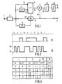
- reference numeral 5 denotes a CMI-decoder unit to whose first input 26 the CMI-encoded input signal, originating from the equalizer 2, is applied.
- the CMI-signal to be equalized is applied to the input 1 of the equalizer 2.
- the output of the equalizer 2 is connected to a first input 12 of a modulo-2 divider 4.
- the output of the equalizer 2 is further connected via a delay element 3 to a second input 13 of the divider 4 which may, for example, be in the form of a double-balanced modulator.
- the output of the equalizer 2 is also connected to an input of the clock regenerator 6, whose output signal controls the CMI-decoder unit 5.
- the output of the divider 4 is connected to a first input 16 of a summing device 7, whose second input 15 is connected to the second terminal 17, i.e. the output of the decoder unit 5.
- the output 14 of the summing device 7 is connected via an integrator 8 to the input of a level detector 9 which has two threshold levels. An alarm signal is supplied from the output 10 of the level detector 9 when the signal applied to its input exceeds one of these two levels.
- the time sequence diagrams give an example of the conversion of a binary signal with logic 1 bits and logic 0 bits (diagram a) into a CMI-encoded signal (diagram b).
- the CMI-code is a 2- level code in which a logic 0 bit is encoded such that each of the two levels E 1 and E 2 is present during half a bit period interval, first E 1 and then E 2 .
- a logic 1 bit is encoded by one of the two levels E 1 or E 2 during an entire bit period interval, and that such that the level changes for consecutive logic 1 bits.
- a CMI-signal of a shape as shown in Fig. 2b is applied to the first input 12 of the divider 4.
- the same signal but delayed through an entire bit period interval is applied to the second input 13 of the divider 4.
- the modulo-2 sum of the two CMI-input signals of the divider 4 is applied to the first input 16 of the summing device 7.
- the decoded CMI-signal which has a shape as shown in Fig. 2a is applied to the second input 15 of the summing device 7.
- the invention is based on the recognition that when the running digital sum of the difference between said binary signal and said modulo-2 sum is determined at the output 14 of the summing device 7, this running digital sum will always be between 0 and 1 for a correctly operating decoder unit 5. This fact is used as the supervision criterium, which will be described in greater detail with reference to Fig. 3.
- the supervision criterium which will be described in greater detail with reference to Fig. 3.
- column I all the possible combinations of the binary signal present at the second input 15 of the summing device 7 are shown in two adjacent entire bit period intevals n.T and (n+1)T, n and (n+1) being the numbers of the time intervals considered and T being the duration of an entire bit period interval.
- Column II (nT) shows the CMI-signal which corresponds to the binary signal shown in column I (nT).
- Column II (n+1 ).T shows the SMI-signal which corresponds to the binary signal shown in column I (n+1 )T.
- the signal from column II ((n+1).T) is applied to the first input 12 of the divider 4 whilst the signal from column 11 (n.T) is applied to the second input 13 of the divider 4, this being the signal supplied T seconds earlier to the first input 12 of the divider 4.
- Column III shows in each square the two modulo-2 sums in the two half-bit period intervals of the CMI-signals of the columns 11 (n+T) and 11 ((n+1).T).
- Column IV shows the running digital sum in the two half-bit intervals of the CMI-signal from column III minus the binary signal from column I (n+1).T.
- Fig. 4a shows any random CMI-signal such as it is applied to the first input 12 of the divider 4. This same CMI-signal is now applied, delayed by a whole bit interval T, to the second input 13 of the divider 4.
- the resultant signal at the output 16 of the divider 4 is shown in Fig. 4c and is equal to the modulo-2 sum of the CMI-signals such as they are shown in Figs. 4a and 4b.
- Fig. 4d shows the decoded binary signal, such as it is present at the output 17 of the decoding unit 5. Let it now be assumed that in the bit intervals T 1 and T 2 an incorrect conversion is effected. In the bit interval T 1 the binary signal should have had the value 0 instead of 1, as shown.
- the binary signal In the bit interval T 2 the binary signal should have had the value 1 instead of 0 as shown.
- the signal occurring at the output 14 of the summing device 7 is shown in Fig. 4e and is the difference between the signals shown in Figs. 4c and 4d.
- This signal is integrated over a number of bit intervals, for example 7 intervals, with the aid of integrator 8.
- the integrated signal has a shape as shown in Fig. 4f by means of a solid line.
- the limits U and L are the two voltage levels to which the level detector 9 is set. Now the level detector 9 will supply an alarm signal from its output 10 at the occurrence of the hatched areas A, B, C and D.
- Fig. 4f shows by means of a dotted line the variation of the integrated signal at the output of the integrator 8 when the decoding unit 5 operates correctly. Consequently, in that case the logic 0 in CMI-code format in the bit period T 1 is converted into a binary logic 0, see Fig. 4d, dotted line. In addition, the logic 1 in CMI-code format in the bit interval T 2 is converted into a binary logic 1, see Fig. 4d, dotted line in bit interval T 2 . Consequently the signal integrated by the integrator 8 remains within the two limits U and L, so that the level detector 9 will not supply an alarm signal from its output 10.
- Fig. 1 shows an embodiment of a method of supervising a CMI-decoding unit. It will be obvious that this manner of supervision is also possible for a CMI-encoding unit in which a binary input signal is converted into a CMI-output signal. In that case the signal flow is from 11 to 1 instead of from 1 to 11, as shown in Fig. 1 for a CMI-decoding unit.
Landscapes
- Engineering & Computer Science (AREA)
- Computer Networks & Wireless Communication (AREA)
- Signal Processing (AREA)
- Physics & Mathematics (AREA)
- Spectroscopy & Molecular Physics (AREA)
- Dc Digital Transmission (AREA)
Claims (2)
Applications Claiming Priority (2)
| Application Number | Priority Date | Filing Date | Title |
|---|---|---|---|
| NL8403366 | 1984-11-06 | ||
| NL8403366A NL8403366A (nl) | 1984-11-06 | 1984-11-06 | Inrichting voor het bewaken van een cmi-codeomvormer. |
Publications (2)
| Publication Number | Publication Date |
|---|---|
| EP0181030A1 EP0181030A1 (fr) | 1986-05-14 |
| EP0181030B1 true EP0181030B1 (fr) | 1990-01-24 |
Family
ID=19844713
Family Applications (1)
| Application Number | Title | Priority Date | Filing Date |
|---|---|---|---|
| EP85201746A Expired EP0181030B1 (fr) | 1984-11-06 | 1985-10-28 | Dispositif pour surveiller un convertisseur de code CMI |
Country Status (5)
| Country | Link |
|---|---|
| US (1) | US4651328A (fr) |
| EP (1) | EP0181030B1 (fr) |
| JP (1) | JPH0824312B2 (fr) |
| DE (1) | DE3575647D1 (fr) |
| NL (1) | NL8403366A (fr) |
Families Citing this family (7)
| Publication number | Priority date | Publication date | Assignee | Title |
|---|---|---|---|---|
| AU621536B2 (en) * | 1987-02-24 | 1992-03-19 | General Electric Capital Corporation | Partial response channel signaling systems |
| JP2550985B2 (ja) * | 1987-04-21 | 1996-11-06 | 日本電気株式会社 | Cmi符号復号器 |
| US4860312A (en) * | 1988-04-12 | 1989-08-22 | Motorola, Inc. | Quality improvement for a digitally transmitted information signal |
| US4928289A (en) * | 1988-12-19 | 1990-05-22 | Systran Corporation | Apparatus and method for binary data transmission |
| JPH02312329A (ja) * | 1989-05-27 | 1990-12-27 | Fujitsu Ltd | 信号伝送方式 |
| US5195110A (en) * | 1991-04-01 | 1993-03-16 | Nec America, Inc. | Clock recovery and decoder circuit for a CMI-encoded signal |
| JP3746232B2 (ja) * | 2001-12-20 | 2006-02-15 | 株式会社日立コミュニケーションテクノロジー | Cmi符号の符号化および復号化方法、cmi符号化回路、およびcmi復号化回路 |
Family Cites Families (10)
| Publication number | Priority date | Publication date | Assignee | Title |
|---|---|---|---|---|
| FR2139665B1 (fr) * | 1971-05-28 | 1973-05-25 | Labo Cent Telecommunicat | |
| US3828346A (en) * | 1972-05-30 | 1974-08-06 | Int Standard Electric Corp | Pcm transmission system |
| GB1489177A (en) * | 1973-10-16 | 1977-10-19 | Gen Electric Co Ltd | Digital data signalling systems and apparatus therefor |
| GB1512700A (en) * | 1975-10-23 | 1978-06-01 | Standard Telephones Cables Ltd | Data transmission |
| GB1563848A (en) * | 1977-02-09 | 1980-04-02 | Hewlett Packard Ltd | Cmi-encoder |
| FR2412990A1 (fr) * | 1977-12-05 | 1979-07-20 | Legras Jacques | Evaluation de la qualite d'une liaison numerique, d'un repeteur regenerateur ou d'un recepteur dans une telle liaison |
| FR2432246A1 (fr) * | 1978-07-26 | 1980-02-22 | Cit Alcatel | Procede et circuit de decodage d'un signal binaire code en cmi |
| DE2836445C2 (de) * | 1978-08-19 | 1979-11-15 | Te Ka De Felten & Guilleaume Fernmeldeanlagen Gmbh, 8500 Nuernberg | Schaltungsanordnung zur Fehlererkennung in Digitalsignalen |
| JPS5825750A (ja) * | 1981-08-07 | 1983-02-16 | Fujitsu Ltd | 二重化時分割通話路の動作照合試験方式 |
| DE3245845A1 (de) * | 1982-12-10 | 1984-06-14 | Siemens AG, 1000 Berlin und 8000 München | Cmi-decoder |
-
1984
- 1984-11-06 NL NL8403366A patent/NL8403366A/nl not_active Application Discontinuation
-
1985
- 1985-10-28 DE DE8585201746T patent/DE3575647D1/de not_active Expired - Lifetime
- 1985-10-28 EP EP85201746A patent/EP0181030B1/fr not_active Expired
- 1985-11-04 US US06/794,864 patent/US4651328A/en not_active Expired - Fee Related
- 1985-11-05 JP JP60246432A patent/JPH0824312B2/ja not_active Expired - Lifetime
Also Published As
| Publication number | Publication date |
|---|---|
| JPS61114637A (ja) | 1986-06-02 |
| DE3575647D1 (de) | 1990-03-01 |
| EP0181030A1 (fr) | 1986-05-14 |
| US4651328A (en) | 1987-03-17 |
| NL8403366A (nl) | 1986-06-02 |
| JPH0824312B2 (ja) | 1996-03-06 |
Similar Documents
| Publication | Publication Date | Title |
|---|---|---|
| US4122300A (en) | Data transmission system and application thereof to the transmission of analog signals and of data in a network with delta modulation | |
| US4267595A (en) | AMI Decoder apparatus | |
| US5394410A (en) | Differentially coded and guard pulse position modulation for communication networks | |
| CA1198824A (fr) | Systeme de transmission de salves | |
| EP0054583B1 (fr) | Méthode pour la transmission de séquences de données binaires et dispositif permettant la détermination rapide de la fin d'une séquence de données binaires transmise | |
| GB2243269A (en) | Decoding binary-coded transmissions | |
| US4425666A (en) | Data encoding and decoding communication system for three frequency FSK modulation and method therefor | |
| EP0166741A1 (fr) | Systeme de communication numerique. | |
| JP2621884B2 (ja) | 通信方法及び符号化装置 | |
| US4651328A (en) | Arrangement for supervising a CMI-code converter | |
| US4276649A (en) | Receiver for digital signals in line code | |
| US4550403A (en) | Method for transmitting a HDBn code signal with an auxiliary binary signal in a digital transmission line and system for monitoring repeaters in the line by means of auxiliary signals | |
| US3457510A (en) | Modified duobinary data transmission | |
| US3953673A (en) | Digital data signalling systems and apparatus therefor | |
| EP0066620B1 (fr) | Circuit de recuperation de signaux d'horloge | |
| US4930127A (en) | Method and device for transmitting a digital engineering service channel by means of the parity channel of a digital bit stream transmitted in a code with parity checking | |
| US4503546A (en) | Pulse signal transmission system | |
| EP0122655B1 (fr) | Système de transmission numérique | |
| US3339142A (en) | Adaptive pulse transmission system with modified delta modulation and redundant pulse elimination | |
| CA2031494C (fr) | Systeme de transmission a codes a correlation | |
| US4876695A (en) | Digital data transmission system having additional bits for auxiliary data | |
| US4928289A (en) | Apparatus and method for binary data transmission | |
| EP0284164B1 (fr) | Unité de décodage pour des signaux à codage CMI | |
| US4110691A (en) | Apparatus and method for detecting errors in a 7-level correlative signal | |
| US5386436A (en) | Synchronization system for use in digital transmission system |
Legal Events
| Date | Code | Title | Description |
|---|---|---|---|
| PUAI | Public reference made under article 153(3) epc to a published international application that has entered the european phase |
Free format text: ORIGINAL CODE: 0009012 |
|
| AK | Designated contracting states |
Kind code of ref document: A1 Designated state(s): CH DE FR GB LI |
|
| 17P | Request for examination filed |
Effective date: 19861105 |
|
| 17Q | First examination report despatched |
Effective date: 19881221 |
|
| GRAA | (expected) grant |
Free format text: ORIGINAL CODE: 0009210 |
|
| AK | Designated contracting states |
Kind code of ref document: B1 Designated state(s): CH DE FR GB LI |
|
| REF | Corresponds to: |
Ref document number: 3575647 Country of ref document: DE Date of ref document: 19900301 |
|
| ET | Fr: translation filed | ||
| PLBE | No opposition filed within time limit |
Free format text: ORIGINAL CODE: 0009261 |
|
| STAA | Information on the status of an ep patent application or granted ep patent |
Free format text: STATUS: NO OPPOSITION FILED WITHIN TIME LIMIT |
|
| 26N | No opposition filed | ||
| REG | Reference to a national code |
Ref country code: CH Ref legal event code: PFA Free format text: PHILIPS ELECTRONICS N.V. |
|
| REG | Reference to a national code |
Ref country code: FR Ref legal event code: CD |
|
| PGFP | Annual fee paid to national office [announced via postgrant information from national office to epo] |
Ref country code: GB Payment date: 19960930 Year of fee payment: 12 |
|
| PGFP | Annual fee paid to national office [announced via postgrant information from national office to epo] |
Ref country code: FR Payment date: 19961022 Year of fee payment: 12 |
|
| PGFP | Annual fee paid to national office [announced via postgrant information from national office to epo] |
Ref country code: DE Payment date: 19961218 Year of fee payment: 12 |
|
| PGFP | Annual fee paid to national office [announced via postgrant information from national office to epo] |
Ref country code: CH Payment date: 19970121 Year of fee payment: 12 |
|
| PG25 | Lapsed in a contracting state [announced via postgrant information from national office to epo] |
Ref country code: GB Free format text: LAPSE BECAUSE OF NON-PAYMENT OF DUE FEES Effective date: 19971028 |
|
| PG25 | Lapsed in a contracting state [announced via postgrant information from national office to epo] |
Ref country code: LI Free format text: LAPSE BECAUSE OF NON-PAYMENT OF DUE FEES Effective date: 19971031 Ref country code: FR Free format text: THE PATENT HAS BEEN ANNULLED BY A DECISION OF A NATIONAL AUTHORITY Effective date: 19971031 Ref country code: CH Free format text: LAPSE BECAUSE OF NON-PAYMENT OF DUE FEES Effective date: 19971031 |
|
| REG | Reference to a national code |
Ref country code: CH Ref legal event code: PL |
|
| GBPC | Gb: european patent ceased through non-payment of renewal fee |
Effective date: 19971028 |
|
| PG25 | Lapsed in a contracting state [announced via postgrant information from national office to epo] |
Ref country code: DE Free format text: LAPSE BECAUSE OF NON-PAYMENT OF DUE FEES Effective date: 19980701 |
|
| REG | Reference to a national code |
Ref country code: FR Ref legal event code: ST |