EP0181043A1 - Feldsensitives Anzeigegerät - Google Patents
Feldsensitives Anzeigegerät Download PDFInfo
- Publication number
- EP0181043A1 EP0181043A1 EP85201788A EP85201788A EP0181043A1 EP 0181043 A1 EP0181043 A1 EP 0181043A1 EP 85201788 A EP85201788 A EP 85201788A EP 85201788 A EP85201788 A EP 85201788A EP 0181043 A1 EP0181043 A1 EP 0181043A1
- Authority
- EP
- European Patent Office
- Prior art keywords
- electrodes
- spaced
- field sensitive
- sensitive material
- impedance
- Prior art date
- Legal status (The legal status is an assumption and is not a legal conclusion. Google has not performed a legal analysis and makes no representation as to the accuracy of the status listed.)
- Withdrawn
Links
- 239000000463 material Substances 0.000 claims abstract description 96
- 230000001939 inductive effect Effects 0.000 claims abstract description 7
- 239000004973 liquid crystal related substance Substances 0.000 claims description 37
- 239000004988 Nematic liquid crystal Substances 0.000 claims description 14
- 230000000903 blocking effect Effects 0.000 claims 1
- 210000004027 cell Anatomy 0.000 description 41
- 210000002858 crystal cell Anatomy 0.000 description 7
- 230000005669 field effect Effects 0.000 description 5
- 239000000203 mixture Substances 0.000 description 4
- 239000004986 Cholesteric liquid crystals (ChLC) Substances 0.000 description 3
- 238000010586 diagram Methods 0.000 description 3
- 230000003287 optical effect Effects 0.000 description 3
- 230000010287 polarization Effects 0.000 description 3
- 239000003989 dielectric material Substances 0.000 description 2
- 239000011521 glass Substances 0.000 description 2
- 230000003068 static effect Effects 0.000 description 2
- 108010010803 Gelatin Proteins 0.000 description 1
- PWHULOQIROXLJO-UHFFFAOYSA-N Manganese Chemical compound [Mn] PWHULOQIROXLJO-UHFFFAOYSA-N 0.000 description 1
- 241000220317 Rosa Species 0.000 description 1
- 239000005083 Zinc sulfide Substances 0.000 description 1
- 230000003213 activating effect Effects 0.000 description 1
- 238000003491 array Methods 0.000 description 1
- 230000005540 biological transmission Effects 0.000 description 1
- 239000000919 ceramic Substances 0.000 description 1
- 230000003098 cholesteric effect Effects 0.000 description 1
- 239000004020 conductor Substances 0.000 description 1
- 230000003467 diminishing effect Effects 0.000 description 1
- 230000000694 effects Effects 0.000 description 1
- 238000005401 electroluminescence Methods 0.000 description 1
- -1 for example Substances 0.000 description 1
- 229920000159 gelatin Polymers 0.000 description 1
- 239000008273 gelatin Substances 0.000 description 1
- 235000019322 gelatine Nutrition 0.000 description 1
- 235000011852 gelatine desserts Nutrition 0.000 description 1
- 238000003384 imaging method Methods 0.000 description 1
- HFGPZNIAWCZYJU-UHFFFAOYSA-N lead zirconate titanate Chemical compound [O-2].[O-2].[O-2].[O-2].[O-2].[Ti+4].[Zr+4].[Pb+2] HFGPZNIAWCZYJU-UHFFFAOYSA-N 0.000 description 1
- 229910052451 lead zirconate titanate Inorganic materials 0.000 description 1
- 239000011344 liquid material Substances 0.000 description 1
- 229910052748 manganese Inorganic materials 0.000 description 1
- 239000011572 manganese Substances 0.000 description 1
- 230000002688 persistence Effects 0.000 description 1
- DRDVZXDWVBGGMH-UHFFFAOYSA-N zinc;sulfide Chemical compound [S-2].[Zn+2] DRDVZXDWVBGGMH-UHFFFAOYSA-N 0.000 description 1
Images

Classifications
-
- G—PHYSICS
- G02—OPTICS
- G02F—OPTICAL DEVICES OR ARRANGEMENTS FOR THE CONTROL OF LIGHT BY MODIFICATION OF THE OPTICAL PROPERTIES OF THE MEDIA OF THE ELEMENTS INVOLVED THEREIN; NON-LINEAR OPTICS; FREQUENCY-CHANGING OF LIGHT; OPTICAL LOGIC ELEMENTS; OPTICAL ANALOGUE/DIGITAL CONVERTERS
- G02F1/00—Devices or arrangements for the control of the intensity, colour, phase, polarisation or direction of light arriving from an independent light source, e.g. switching, gating or modulating; Non-linear optics
- G02F1/01—Devices or arrangements for the control of the intensity, colour, phase, polarisation or direction of light arriving from an independent light source, e.g. switching, gating or modulating; Non-linear optics for the control of the intensity, phase, polarisation or colour
- G02F1/13—Devices or arrangements for the control of the intensity, colour, phase, polarisation or direction of light arriving from an independent light source, e.g. switching, gating or modulating; Non-linear optics for the control of the intensity, phase, polarisation or colour based on liquid crystals, e.g. single liquid crystal display cells
- G02F1/133—Constructional arrangements; Operation of liquid crystal cells; Circuit arrangements
- G02F1/1333—Constructional arrangements; Manufacturing methods
- G02F1/1343—Electrodes
- G02F1/134309—Electrodes characterised by their geometrical arrangement
- G02F1/134336—Matrix
-
- G—PHYSICS
- G02—OPTICS
- G02F—OPTICAL DEVICES OR ARRANGEMENTS FOR THE CONTROL OF LIGHT BY MODIFICATION OF THE OPTICAL PROPERTIES OF THE MEDIA OF THE ELEMENTS INVOLVED THEREIN; NON-LINEAR OPTICS; FREQUENCY-CHANGING OF LIGHT; OPTICAL LOGIC ELEMENTS; OPTICAL ANALOGUE/DIGITAL CONVERTERS
- G02F1/00—Devices or arrangements for the control of the intensity, colour, phase, polarisation or direction of light arriving from an independent light source, e.g. switching, gating or modulating; Non-linear optics
- G02F1/01—Devices or arrangements for the control of the intensity, colour, phase, polarisation or direction of light arriving from an independent light source, e.g. switching, gating or modulating; Non-linear optics for the control of the intensity, phase, polarisation or colour
- G02F1/13—Devices or arrangements for the control of the intensity, colour, phase, polarisation or direction of light arriving from an independent light source, e.g. switching, gating or modulating; Non-linear optics for the control of the intensity, phase, polarisation or colour based on liquid crystals, e.g. single liquid crystal display cells
- G02F1/133—Constructional arrangements; Operation of liquid crystal cells; Circuit arrangements
- G02F1/1333—Constructional arrangements; Manufacturing methods
- G02F1/1345—Conductors connecting electrodes to cell terminals
-
- G—PHYSICS
- G02—OPTICS
- G02F—OPTICAL DEVICES OR ARRANGEMENTS FOR THE CONTROL OF LIGHT BY MODIFICATION OF THE OPTICAL PROPERTIES OF THE MEDIA OF THE ELEMENTS INVOLVED THEREIN; NON-LINEAR OPTICS; FREQUENCY-CHANGING OF LIGHT; OPTICAL LOGIC ELEMENTS; OPTICAL ANALOGUE/DIGITAL CONVERTERS
- G02F1/00—Devices or arrangements for the control of the intensity, colour, phase, polarisation or direction of light arriving from an independent light source, e.g. switching, gating or modulating; Non-linear optics
- G02F1/01—Devices or arrangements for the control of the intensity, colour, phase, polarisation or direction of light arriving from an independent light source, e.g. switching, gating or modulating; Non-linear optics for the control of the intensity, phase, polarisation or colour
- G02F1/13—Devices or arrangements for the control of the intensity, colour, phase, polarisation or direction of light arriving from an independent light source, e.g. switching, gating or modulating; Non-linear optics for the control of the intensity, phase, polarisation or colour based on liquid crystals, e.g. single liquid crystal display cells
- G02F1/133—Constructional arrangements; Operation of liquid crystal cells; Circuit arrangements
- G02F1/1333—Constructional arrangements; Manufacturing methods
- G02F1/1347—Arrangement of liquid crystal layers or cells in which the final condition of one light beam is achieved by the addition of the effects of two or more layers or cells
Definitions
- the present invention relates to a field sensitive display device for forming a display when subjected to visible light comprising a field sensitive material, spaced electrodes for inducing a field therebetween, means for containing the field sensitive material and the spaced electrodes with the field sensitive material being relatively disposed between the spaced electrodes in order that a field induced by the spaced electrodes across the field sensitive material is capable of affecting the field sensitive material, a first of the spaced electrodes including an elongated impedance element and a plurality of elongated conductive, substantially low impedance portions spaced with respect to one another along their length, the plurality of low impedance portions being connected to different electrical locations disposed along the length of the impedance element and extending therefrom, first terminal means connected to the ends of the elongated impedance element for applying a first electrical signal thereto, a second of the spaced electrodes including a conductive substantially low impedance layer, and a second terminal means connected to the second electrode for applying a second electrical signal thereto
- the invention is therefore in the field of field sensitive optical displays, particularly of the field effect and field excited types, and to the generation of the fields for activating the displays and to the scanning of displays. More particularly, the invention concerns liquid crystal, optoceramic and electroluminescence displays, and electrode and scanning arrangements therefor.
- the present invention contemplates utilization of liquid crystal materials in which the propagation or characteristics of light incidence thereon can be altered by inducing an electric or magnetic field in the liquid crystal material.
- liquid crystal materials include, but are not limited to, nematic liquid crystal materials possessing dynamic or quiescent scattering, or twisted field-effect electro-optical properties, and the mixtures of those nematic liquid crystal materials with cholesteric liquid crystal materials.
- a dynamic scattering liquid crystal material In a dynamic scattering liquid crystal material, light is transmitted substantially unaffected through the material in the absence of a field. When a field of sufficient magnitude is induced in the liquid crystal material, light incident upon the material is optically scattered and transmission of light through the material is substantially prevented.
- a quiescent scattering liquid crystal material possesses field effect electro-optical properties which are the converse of those of the dynamic scattering liquid crystal, that is, in the absence of a field, the quiescent scattering liquid crystal material scatters incident light, while a field induced in the quiescent liquid crystal material causes it to transmit incident light therethrough.
- a twisted nematic liquid crystal material layers of molecules at opposed surfaces of the material can be caused to be aligned at an angle with each other in the absence of a field.
- the molecules between the opposed surfaces have varying angular alignments with the result that the molecular orientation through the material from one surface to the other is helical or "twisted".
- the plane of polarization of plane polarized light is rotated by the angle formed by the opposed surface molecules as the light passes through the liquid crystal material in the absence of a field.
- the application of a field to the material destroys the twisted alignment of the molecules with the result that the material transmits incident plane polarized light therethrough without substantial rotation of the plane of polarization.
- nematic and cholesteric liquid crystal materials provide a storage characteristic to the scattering nematic liquid crystal materials. Such mixtures retain field-induced electro-optical characteristics after the field is removed. The application of an appropriate ac (alternating current) field returns the material to the state it normally possesses in the absence of a field.
- ac alternating current
- Liquid crystal materials of the types referred to, as well as others, are well known in the prior art. See, for example, S. Sherr, “Electronic Displays”, John Wiley & Sons, New York, 1979; G. Heilmeier, “Liquid-Crystal Display Device”, Scientific American, April, 1970, pp. 100-106; G. Heilmeier, L. Zanoni & L. Barton, "Dynamic Scattering: A New Electrooptic Effect in Certain Classes of Nematic Liquid Crystals", Proceedings of the IEEE, Vol. 56, No. 7, July 1968, pp. 1162-1171; and U.S. Patent No. 3,918,796 on November 11, 1975 to Fergason.
- Nematic scattering liquid crystal electro-optical elements are well known in the prior art, as described, for example, in U.S. Patent No. 3,322,458, issued on May 30, 1967, to Williams. Twisted liquid crystal electro-optical elements which require the use of polarizing elements, are also well known in the prior art, as described, for example, in the aforementioned '796 Fergason patent.
- the Fergason '796 patent and U.S. Patent No. 3,834,792, issued on September 10, 1976, to Janning, describe two arrangements for aligning liquid crystal molecules in a display in order that polarized light passing through the material in the absence of a field is rotated.
- the Fergason '796 patent teaches rubbing each of the glass plates which enclose the liquid crystal material in a single predetermined direction and thereafter positioning the plates with the directions of rubbing of the plates forming an angle through which the polarized light is to be rotated.
- the Janning '792 patent teaches the growth of an alignment film on each plate and then the arranging of the plates with the directions of growth on each of the plates forming a desired angle with respect to one another.
- Both the Fergason '796 and the Janning '792 patents disclose arrangements of polarizers and twisted liquid crystal cells.
- the '875 patent also discloses scanning devices incorporating such dielectrics.
- the disclosure of the '875 patent is incorporated herein by reference.
- the '875 patent also discloses display cells having both a resistive electrode in which a voltage gradient can be generated and a conductive electrode. By applying suitable control voltages to such cells and combination of such cells, displays can be formed which include those having a movable dot or line. Sequential scanning of such cells can provide displays comprising patterns or images.
- U.S. Patent No. 3,675,988, issued on July 11, 1972, to Soref discloses liquid crystal display devices in which a variety of images, such as a moving bright spot, a variable length bar, a moving arrow and a moving window, can be generated.
- the Soref '988 patent discloses a liquid crystal display device which includes transparent electrodes uniformly coated on the surface of opposed plates enclosing the liquid crystal material.
- One of the electrodes has high resistivity with the result that a voltage gradient can be generated along the extent of the electrode, i.e. each line location of the electrode will have a different voltage level.
- U.S. Patent No. 3,807,831 issued on April 30, 1974 to Soref discloses a liquid crystal display device which includes interleaved arrays of alternate parallel electrodes. A field is induced between interleaved electrodes.
- a field sensitive display device for forming a display when subjected to visible light comprising a field sensitive material, first and second spaced electrodes each of the spaced electrodes being disposed in a different plane spaced apart from one another for inducing a field therebetween, means for containing the field sensitive material and the spaced electrodes with the field sensitive material being relatively disposed between the spaced electrodes in order that a field induced by the spaced electrodes across the field sensitive material is capable of affecting the field sensitive material, a first of the spaced electrodes including an elongated impedance element and a plurality of elongated conductive, substantially low impedance portions spaced with respect to one another along their length, the plurality of low impedance portions being connected to different electrical locations disposed along the length of the impedance element and extending therefrom, first terminal means connected to the ends of the elongated impedance element for applying a first electrical signal thereto, a second of the spaced electrodes including an elongated im
- the description which follows hereinafter, of embodiments of the invention indicates how the invention provides simplified field sensitive optical devices for displaying, inter alia, a movable dot, having a reduced number of terminals for selectively inducing fields in such display devices for scanning such devices to provide desired images, e.g. intersecting line images which can be moved independently of one another or a line image capable of pivotal movement.
- the present invention also enables the response time and life of liquid crystal display devices to be improved, the electrode structures and address arrangements for the devices to be simplified and the superimposition of varying and dc fields in the field sensitive material.
- the invention yields displays which utilize field sensitive materials and relatively simple addressing arrangements comprising a reduced number of terminals for inducing fields in or upon the material.
- Each of the electrodes includes an impedance portion disposed in a non-active region in order to avoid affecting the field sensitive material, and a plurality of conductive, substantially low impedance elements extending in an active region in order to affect directly the field sensitive material.
- Each low impedance portion is in electrical contact with the impedance portion at a different impedance location thereof and extends therefrom. Only two terminals are required for the impedance electrode, i.e. one at each end of the impedance portion. An additional terminal may be provided for a capacitance disposed directly in contract with the low impedance portions.
- Devices having arrangements of such electrodes can provide a plurality of different displays by utilizing relatively simple addressing and scanning arrangements.
- the impedance portion is substantially resistive and the low impedance portions are substantially non-resistive.
- respective electrodes and portions may be impedance or low impedance, respectively.
- opposed plates contain the field sensitive material and the electrodes are disposed in, on or adjacent the plates or in, on or adjacent the field sensitive material. The electrodes may be spaced with the field sensitive material therebetween, or substantially co-planar and disposed in or adjacent to the field sensitive material.
- both of the electrodes include a resistive portion with conductive, substantially non-resistive elements or portions connected thereto disposed in, on or adjacent to opposed plates, the conductive elements extending either transversely to each other in a grid pattern or parallel to each other.
- Selectively addressing the electrodes in accordance with the invention provides selected regions bounded by conductive elements to be made to contrast other regions.
- the electrodes are disposed substantially in a common plane in or adjacent to the field sensitive material with the non-resistive elements of one electrode interleaved with those of the other electrode. Selectively addressing the electrodes provides selected regions extending transversely of adjacent interleaved non-resistive elements to be made to contrast other regions.
- the aforementioned display embodiments may provide displays of a movable dot, individually movable intersecting lines, a pivoting line and other displays by means of various addressing schemes and various arrangements of the cells alone or with other optical elements, such as polarizers.
- Liquid crystal material may be utilized as the field sensitive material.
- the field sensitive material is an optoceramic or an electroluminescent material.
- various electrode structures are described for use with field-effect material, in particular, liquid crystal and optoceramic material. It will, however, be understood that such electrode structures can also be used in other field-sensitive materials, for example, field-excited materials such as, for example, electroluminescent materials.
- Liquid crystal cells are illustrated in Fig. 1 and optoceramic cells are illustrated in Figs. 5,6 and 7 which include improved electrode structures.
- Various display patterns in accordance with the invention can be obtained utilizing cells according to the invention as illustrated in Figs. 2,3,3A and 4. Such illustrated displays and others described herein are intended to be exemplary and not exhaustive.
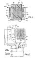
- a field sensitive cell 90 is depicted in which electrodes 14A,14B are disposed on each of the plates 91 and 92.
- the conductive strips 28 of the opposed electrodes 14A,14B extend perpendicular to each other, thereby forming a grid pattern.
- Capacitances 34' are disposed in contact with the strips 28 of the respective electrode.
- Terminals 30A,30B and 31A,31B are connected to ends of respective resistive portion 24A,24B of each of the electrodes, while terminals 38A,38B are connected to the respective capacitance strips 34' disposed on each of the electrodes.
- the opposed plates 91,92 are offset in order that the capacitance strips 34' are in the non-active region of the cell 90.
- capacitances 34 and 36 can be provided for cell 90 as described in EP-A-0044637.
- FIG. 2 an embodiment of the invention is schematically illustrated in which the cell 90 is utilized.
- the terminals 30A,31A,30B,31B of each of the resistive portions 24A,24B of each of the electrodes 14A,14B are connected to respective poles of switches 93-96.
- the switches 93-96 are ganged to operate in unison.
- Contact 97 of switch 93 is connected to the positive supply 99 and contact 101 of switch 93 is connected to a variable dc supply 103.
- Contact 105 of switch 94 is also connected to the variable dc supply 103 and to contact 101.
- Contact 107 of switch 94 is connected to the negative dc supply 109.
- switch 95 has a contact connected to the positive supply and a contact connected to the variable dc supply.
- Switch 96 has a contact connected to the negative supply and a contact connected to the variable dc supply with the contacts 112,113 of switches 95 and 96 being connected together and to the variable dc supply.
- switches 93-96 In operation, in one position of switches 93-96, one of the electrodes is operated as an address electrode while the other electrode is operated on the load electrode. In the other position of switches 93-96, the load and address electrodes are reversed.
- a twisted nematic liquid crystal material is contained in cell 90 and the magnitude of the positive and negative voltage supplies can be five volts.
- electrode 14A is the address electrode and electrode 14B is the load electrode.
- Positive 5 volts is applied to terminal 30A of resistive portion 24A of electrode 14A and negative 5 volts is imposed at electrode 31A of resistive portion 24A.
- ten conductive strips have been shown for each of the electrodes. The voltage at each of the conductive strips for electrode 14A is indicated, +5 and -5 volts being present at the right-most and left-most conductive strips, respectively, with the voltages on each of the other strips diminishing toward the center.
- the central strip has zero volts.
- Terminals 30B and 31B of electrode 14B are connected together and to the variable dc source 103. Since essentially no current flows through the electrode 14B from source 103, each of the conductive strips and each portion of the resistive portion 24B will be at the same voltage. The variable dc voltage applied to electrode 14B therefore appears simultaneously across all of the conductive strips.
- a series of zero potential points is generated at the intersection of conductive strips which are at the same potential.
- a series of zero potential points is generated extending vertically through the center of the cell.
- the moving point or dot can be used as a scanning device. In one switch position, scanning in the X direction is carried out, while in the other switch position, scanning in the Y direction is carried out.
- the turn-off time of the liquid crystal material is relatively slow compared to the turn-on time, the turn-off time acts like a persistence, and the entire display can be scanned before the liquid crystal material turns off.
- This feature of the invention permits operation of the display for imaging.
- Computer or microprocessor controls can be utilized for voltage generation and switching to provide scanning and image display.
- terminals 30A,31B of each of the electrodes 14A,14B of cell 90 are connected together and to ground.
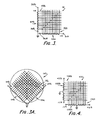
- the cell 90 in Fig. 3 is capable of providing a pivoting or swinging line display.
- Each of the terminals 31A,30B is connected to a variable dc source of the same polarity.
- an equal voltage of sufficient magnitude for example 5 volts for twisted nematic liquid crystal material
- a series of zero potential points are generated at the intersection of the conductive strips along the diagonal of the cell.
- the cell 90 in Fig. 3 can be used as a meter 110 as shown in Fig. 3A in which the line formed by the dots is the meter needle.
- Static information such as values of the parameter being measured associated with the indication lines 112 can be disposed on the cell.
- the static information can be provided in the display by removing selected areas of the polarizers. Thus, light passing through the selected areas in the polarizers will not be blocked.
- a cell 20 can be utilized as a meter display.
- Cell 120 includes electrodes 114A and 114B in which the resistive portions 124A,124B thereof are grounded in the center.
- Cell 120 can provide a pivoting line display which pivots 360° about the center of the display rather than 90° about a corner of the display as in Fig. 3.
- the display of Fig. 4 can be used for a meter in which the needle is pivotable over a full 360° range. Only half of the needle in Fig. 4 is displayed, one half of the needle being blocked out when it is an inactive quadrant. A positive and a negative voltage is applied to respective terminals of the resistive portions. Otherwise, the display of Fig. 4 operates similarly to the display of Fig. 3.
- the display device 150 utilizes an optoceramic material 152, for example piezoelectric lead zirconate titanate (PLZT), as the field sensitive material.
- PZT piezoelectric lead zirconate titanate
- the optoceramic material rotates the plane of plane polarized light passing therethrough by 90° in the presence of a field and transmits plane polarized light therethrough substantially unrotated in the absence of an appropriate field.
- cell 150 includes opposed, transparent spaced plates 154,155 preferably of glass. Interposed between the plates is a gelatin material 157 which supports therein a wafer 152 of optoceramic material. Electrodes 14 are disposed on opposed surfaces of or imbedded within opposed sides of the wafer. The conductive portions 28 of electrodes 14 face and extend parallel to each other and induce fields in wafer regions bounded on each side by pairs of the conductive strips. The resistive portions 24 are disposed in non-active regions of the cell.
- Polarizers can be disposed adjacent the sides of cell 150 to provide desired displays, the polarizers being positioned so that the planes of polarization are at a 45° angle.
- Cell 150 is addressed as above described in connection with other cells to obtain displays as described above and other displays.
- the magnitude of the voltage applied to the cell electrodes to induce a field in the presence of which plane polarized light is transmitted unrotated is from about 0 to about 800 volts, depending on the thickness of the wafer and the particular optoceramic material.
- the electrodes 14 of cell 150A may both be disposed in the same plane on a surface of or imbedded within the optoceramic material with the conductive strips 28 interleaved. This arrangement induces transverse fields between adjacent interleaved strips, the fields extending into the optoceramic material between adjacent conductive strips.
- Cells 150 and 150A may also comprise other electrode arrangements as described above and the cells described above may comprise the electrode arrangements of cells 150,150A.
- Certain cells have been described in connection with twisted nematic liquid crystal material. It will be understood that such cells may operate with a dynamic or quiescent scattering liquid crystal material to obtain certain of the display patterns described herein and other display patterns.
- electroluminescent materials which can be employed include zinc sulphide doped with manganese. Such materials can generate light at 300 volts ac while being unexcited at dc voltages and at lower ac voltages.
- the displays can otherwise be generated as described above.
Landscapes
- Physics & Mathematics (AREA)
- Nonlinear Science (AREA)
- Mathematical Physics (AREA)
- Chemical & Material Sciences (AREA)
- Crystallography & Structural Chemistry (AREA)
- General Physics & Mathematics (AREA)
- Optics & Photonics (AREA)
- Geometry (AREA)
- Liquid Crystal (AREA)
- Liquid Crystal Display Device Control (AREA)
- Control Of Indicators Other Than Cathode Ray Tubes (AREA)
Applications Claiming Priority (2)
| Application Number | Priority Date | Filing Date | Title |
|---|---|---|---|
| US16575380A | 1980-07-03 | 1980-07-03 | |
| US165753 | 1980-07-03 |
Related Parent Applications (1)
| Application Number | Title | Priority Date | Filing Date |
|---|---|---|---|
| EP81302985.7 Division | 1981-07-01 |
Publications (1)
| Publication Number | Publication Date |
|---|---|
| EP0181043A1 true EP0181043A1 (de) | 1986-05-14 |
Family
ID=22600312
Family Applications (2)
| Application Number | Title | Priority Date | Filing Date |
|---|---|---|---|
| EP85201788A Withdrawn EP0181043A1 (de) | 1980-07-03 | 1981-07-01 | Feldsensitives Anzeigegerät |
| EP19810302985 Expired EP0044637B1 (de) | 1980-07-03 | 1981-07-01 | Feldstärkeabhängige optische Anzeigen, Erzeugung der elektrischen Felder und Abtastung der Anzeigen |
Family Applications After (1)
| Application Number | Title | Priority Date | Filing Date |
|---|---|---|---|
| EP19810302985 Expired EP0044637B1 (de) | 1980-07-03 | 1981-07-01 | Feldstärkeabhängige optische Anzeigen, Erzeugung der elektrischen Felder und Abtastung der Anzeigen |
Country Status (4)
| Country | Link |
|---|---|
| EP (2) | EP0181043A1 (de) |
| JP (1) | JPS5774786A (de) |
| CA (1) | CA1197638A (de) |
| DE (1) | DE3176485D1 (de) |
Families Citing this family (1)
| Publication number | Priority date | Publication date | Assignee | Title |
|---|---|---|---|---|
| GB2327797A (en) * | 1997-07-31 | 1999-02-03 | Sharp Kk | Spatial light modulator and display |
Citations (6)
| Publication number | Priority date | Publication date | Assignee | Title |
|---|---|---|---|---|
| US3645604A (en) * | 1970-08-10 | 1972-02-29 | Bell Telephone Labor Inc | Liquid crystal display |
| US3675988A (en) * | 1969-11-25 | 1972-07-11 | Sperry Rand Corp | Liquid crystal electro-optical measurement and display devices |
| FR2145910A5 (de) * | 1971-07-15 | 1973-02-23 | Int Liquid Xtal Co | |
| US3820875A (en) * | 1972-04-14 | 1974-06-28 | W Bohmer | Scanner devices utilizing field effect light scattering dielectrics |
| US3834794A (en) * | 1973-06-28 | 1974-09-10 | Beckman Instruments Inc | Liquid crystal electric field sensing measurement and display device |
| US3918796A (en) * | 1971-02-09 | 1975-11-11 | Hoffmann La Roche | Liquid-crystal non-linear light modulators using electric and magnetic fields |
-
1981
- 1981-06-30 CA CA000380960A patent/CA1197638A/en not_active Expired
- 1981-07-01 EP EP85201788A patent/EP0181043A1/de not_active Withdrawn
- 1981-07-01 EP EP19810302985 patent/EP0044637B1/de not_active Expired
- 1981-07-01 DE DE8181302985T patent/DE3176485D1/de not_active Expired
- 1981-07-03 JP JP10434881A patent/JPS5774786A/ja active Pending
Patent Citations (6)
| Publication number | Priority date | Publication date | Assignee | Title |
|---|---|---|---|---|
| US3675988A (en) * | 1969-11-25 | 1972-07-11 | Sperry Rand Corp | Liquid crystal electro-optical measurement and display devices |
| US3645604A (en) * | 1970-08-10 | 1972-02-29 | Bell Telephone Labor Inc | Liquid crystal display |
| US3918796A (en) * | 1971-02-09 | 1975-11-11 | Hoffmann La Roche | Liquid-crystal non-linear light modulators using electric and magnetic fields |
| FR2145910A5 (de) * | 1971-07-15 | 1973-02-23 | Int Liquid Xtal Co | |
| US3820875A (en) * | 1972-04-14 | 1974-06-28 | W Bohmer | Scanner devices utilizing field effect light scattering dielectrics |
| US3834794A (en) * | 1973-06-28 | 1974-09-10 | Beckman Instruments Inc | Liquid crystal electric field sensing measurement and display device |
Also Published As
| Publication number | Publication date |
|---|---|
| DE3176485D1 (en) | 1987-11-19 |
| EP0044637A1 (de) | 1982-01-27 |
| EP0044637B1 (de) | 1987-10-14 |
| JPS5774786A (en) | 1982-05-11 |
| CA1197638A (en) | 1985-12-03 |
Similar Documents
| Publication | Publication Date | Title |
|---|---|---|
| US4493531A (en) | Field sensitive optical displays, generation of fields therefor and scanning thereof | |
| JP4523083B2 (ja) | 液晶表示装置 | |
| KR100531928B1 (ko) | 액정디스플레이 | |
| US4529271A (en) | Matrix addressed bistable liquid crystal display | |
| US4917475A (en) | Flexoelectric liquid crystal device | |
| KR970028772A (ko) | 액티브 매트릭스형 액정표시소자 | |
| US3781085A (en) | Liquid crystal display | |
| US4449125A (en) | Matrix display device | |
| US3834794A (en) | Liquid crystal electric field sensing measurement and display device | |
| JPH09197420A (ja) | 液晶素子 | |
| KR101499241B1 (ko) | 액정 표시 장치 | |
| EP0083822A1 (de) | Flüssigkristall-Anzeigevorrichtung | |
| US7599036B2 (en) | In-plane switching active matrix liquid crystal display apparatus | |
| US4641923A (en) | Field sensitive optical displays with electrodes with high and low impedance portions | |
| TWI237728B (en) | Liquid crystal display | |
| US4113352A (en) | Electro-optic matrix display | |
| EP0181043A1 (de) | Feldsensitives Anzeigegerät | |
| JP2001083521A (ja) | 液晶表示装置 | |
| US4116543A (en) | Control electro-optical device utilizing liquid crystal | |
| JP3013260B2 (ja) | 液晶装置 | |
| RU2017184C1 (ru) | Способ управления многоэлементным электрооптическим преобразователем и многоэлементный электрооптический преобразователь | |
| CA1230945A (en) | Field sensitive optical displays, generation of fields therefor and scanning thereof | |
| RU2017183C1 (ru) | Способ управления многоэлементным электрооптическим преобразователем и многоэлементный электрооптический преобразователь | |
| JPH11258616A (ja) | 液晶表示素子 | |
| JPH04502066A (ja) | 隣接画像素子間の可視的間隙のない液晶表示装置 |
Legal Events
| Date | Code | Title | Description |
|---|---|---|---|
| PUAI | Public reference made under article 153(3) epc to a published international application that has entered the european phase |
Free format text: ORIGINAL CODE: 0009012 |
|
| 17P | Request for examination filed |
Effective date: 19851114 |
|
| AC | Divisional application: reference to earlier application |
Ref document number: 44637 Country of ref document: EP |
|
| AK | Designated contracting states |
Kind code of ref document: A1 Designated state(s): BE CH DE FR GB IT LI NL SE |
|
| 17Q | First examination report despatched |
Effective date: 19880114 |
|
| RAP1 | Party data changed (applicant data changed or rights of an application transferred) |
Owner name: CONTROL INTERFACE CORPORATION |
|
| STAA | Information on the status of an ep patent application or granted ep patent |
Free format text: STATUS: THE APPLICATION IS DEEMED TO BE WITHDRAWN |
|
| 18D | Application deemed to be withdrawn |
Effective date: 19890201 |
|
| RIN1 | Information on inventor provided before grant (corrected) |
Inventor name: HOFFMAN, LOUIS S. Inventor name: BETANCOURT, WALTER J. Inventor name: BOHMER, WILLIAM |