EP0181187A2 - Appareil de conversion de puissance - Google Patents
Appareil de conversion de puissance Download PDFInfo
- Publication number
- EP0181187A2 EP0181187A2 EP85307998A EP85307998A EP0181187A2 EP 0181187 A2 EP0181187 A2 EP 0181187A2 EP 85307998 A EP85307998 A EP 85307998A EP 85307998 A EP85307998 A EP 85307998A EP 0181187 A2 EP0181187 A2 EP 0181187A2
- Authority
- EP
- European Patent Office
- Prior art keywords
- output
- error amplifier
- signal
- chopper
- produces
- Prior art date
- Legal status (The legal status is an assumption and is not a legal conclusion. Google has not performed a legal analysis and makes no representation as to the accuracy of the status listed.)
- Granted
Links
Images

Classifications
-
- H—ELECTRICITY
- H02—GENERATION; CONVERSION OR DISTRIBUTION OF ELECTRIC POWER
- H02M—APPARATUS FOR CONVERSION BETWEEN AC AND AC, BETWEEN AC AND DC, OR BETWEEN DC AND DC, AND FOR USE WITH MAINS OR SIMILAR POWER SUPPLY SYSTEMS; CONVERSION OF DC OR AC INPUT POWER INTO SURGE OUTPUT POWER; CONTROL OR REGULATION THEREOF
- H02M7/00—Conversion of AC power input into DC power output; Conversion of DC power input into AC power output
- H02M7/42—Conversion of DC power input into AC power output without possibility of reversal
- H02M7/44—Conversion of DC power input into AC power output without possibility of reversal by static converters
- H02M7/48—Conversion of DC power input into AC power output without possibility of reversal by static converters using discharge tubes with control electrode or semiconductor devices with control electrode
Definitions
- This invention relates to power converter apparatus which utilises a DC power source having large fluctuations in voltage such as a solar battery or the like.
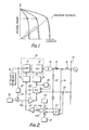
- a solar battery has voltage-current characteristics and power-current characteristics as shown in Figure 1 of the accompanying drawings, wherein insolation quantities are defined as parameters.
- the voltage current characteristics are shown by solid lines and the power-current characteristics are shown by dotted lines and both sets of characteristics indicate that both the current and power increase as the insolation quantity increases.
- a solar battery has the disadvantages that, due to its large fluctuations in voltage, power to be supplied decreases when excessive amount of current is drawn.
- power to be supplied decreases when excessive amount of current is drawn.
- the maximum voltage for various insolation quantities is maintained substantially constant.
- a power converter apparatus constituted by a chopper and an inverter to utilise a solar battery in order to supply power to a load or power system.
- Installation of the chopper at the DC input of the inverter allows the chopper to perform a constant output voltage control, and the inverter to perform such a control that a pulse width is maintained at a specified value, whereby the harmonics components in the output voltage of the inverter are reduced.
- a solar battery In a power converter system that utilises a solar battery for a power source, there is substantially no period throughout the year in which the power converter apparatus receives an output of maximum power from the solar battery, i.e., the period to perform a full load operation, and the averaged load factor thereof throughout a year is approximately 20 to 80 %, so that the efficiency in a light-load operation of the power converter apparatus is regarded as of major importance.
- a solar battery has an extremely high manufacturing cost per kw, so that it is particularly significant to reduce the loss of the power converter apparatus as compared to a system that utilises a power source, such as a storage battery.
- the chopper can achieve advantages, such as compactness of the output filter circuit and simplification of the contral circuit, whereas this produces disadvantages, such that the loss developed by switching the DC circuit with the chopper is not reduced, even in a light-load operation.
- the total loss P T of the switching elements can be expressed by the following equation: where P S represents a loss in steady ON state,
- the steady ON state loss P s of the second term is proportional to a steady ON current
- the first term (P ON + P OFF ) x f is a component proportional to the switching frequency f.
- the loss of the chopper can be separated into a fixed loss of the first term and a load loss of the second term, and there is provided such a disadvantage that, when the power converter apparatus is in a light-load operation, the proportion of the fixed loss becomes greater, whereby the efficiency of the power converter apparatus is reduced.
- a power converter apparatus comprises a chopper connectible to a DC power source; and an inverter connected to receive the DC output of the chopper and to supply converted AC power to a load; characterised in that an error amplifier is connected to detect the output voltage of the apparatus and to compare it with a predetermined reference value; an oscillator serves to produce a signal having a frequency representative of the output of the error amplifier; and a phase shifter produces a signal of variable pulse width varied in synchronism with the output signal of the oscillator for controlling the chopper.
- the power converter apparatus 13 is constituted by a chopper 11 and an inverter 12. Connection of the chopper 11 at the DC input of the inverter 12 allows the chopper 11 to perform a constant output voltage control, and the inverter 12 is to perform such a control that a pulse width is maintained to a specified value, whereby the harmonics components in the output voltage of the inverter 12 are reduced.
- a voltage reference 40 and an inverter output voltage 22 are compared-so as to produce a difference signal on line 44a which, in turn, is fed through a changeover switch 44 into an error amplifier 43.
- a reactive power reference 41 and an output of a reactive power transducer 42 are compared so as to produce a difference signal on line 44b which, in turn, is fed through the changeover switch 44 into the error amplifier 43, an output of which is fed into a voltage control circuit 45 which generates a gate signal for the chopper 11.
- numerals 455 and 456 represent function generators that convert the output signal of the error amplifier circuit 43.
- Reference 457 is a V/F converter that converts the output signal from the function generator 456 into a frequency proportional thereto
- 452 is a triangular waveform generator that generates a triangular waveform signal in synchronism with the frequency from the V/F converter 457
- 451 is a comparator that compares the output signals of the triangular waveform generator 452 and the function generator 455, respectively.
- the comparator 451 and the triangular waveform generator 452 together constitute a phase shifter 50.
- the function generator 456 has characteristics as shown in Figure 4. Within a region in which the output of the error amplifier 43 is smaller than a specified input level e o , the function generator 456 produces an output that increases in proportion to the output of the error amplifier 43, while, above the specified level e o , a constant output signal e 1 is produced.
- the V/F converter 457 produces a frequency proportional to the output signal of the function generator 456, namely its output frequency increases or remains constant depending upon whether the output of the error amplifier 43 is below or above the specified level e o .
- the function generator 455 has characteristics as shown in Figure 5 where, within a region in which the output of the error amplifier 43 is smaller than the specified input level e o , the function generator 455 produces a constant output signal e 2 while, above the specified level e o , it produces an output that increases in proportion to the output from the error amplifier 43.
- the triangular waveform generator 452 receives an output signal from an oscillator so as to produce a triangular waveform signal in synchronism with the output signal as shown in Figure 6.
- the output signals of the triangular waveform generator 452 and the error amplifier 43 are fed into the comparator 451 so as to be compared in magnitude with each other.
- f shows the output signal of the V/F converter 457 and the frequency thereof is varied in accordance with characteristics shown in Figure 4.
- G shows an output signal G 2 of the triangular waveform generator 452 and an output signal G 1 of the function generator 455 that has the characteristics shown in Figure 5, and, during periods when the latter is greater than the former, the comparator 451 produces an output signal of "1" state, as shown in Figure 6 H.
- the output signal H of the comparator 451 is in "1" state, it causes the switching elements of the chopper 11 to be conductive through a drive circuit 454.
- the output signal of the triangular waveform generator 452 has a constant slope so that, in accordance with the magnitude of the output signal of the error amplifier 43, the comparison threshold level of the comparator 451 varies such that the conduction period of the switching element is varied.
- the solar battery voltage is detected through a DC amplifier 20 that insulates the control circuit 100 from the main circuit and also adjusts the voltage gain.
- the thus detected DC voltage value 21 is compared with a DC voltage reference 30 so as to produce a difference signal on line 31a which, in turn, is fed into an error amplifier 31.
- Reference numeral 32 designates a so-called PLL (phase locked loop) circuit that receives three separate signals such as a signal a which is an output of the error amplifier 31, a signal b which is a phase reference signal derived from a voltage 23 of the power system 17, and a signal c which is an output of a frequency divider 33 that divides the output frequency of the PLL circuit 32.
- PLL phase locked loop
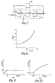
- FIG. 7 is a block diagram illustrating an example of the PLL circuit 32, which is constituted by a phase error detector PHP, a low pass filter LPF, and a voltage controlled oscillator VCO.
- the phase error detector PHD produces a signal d proportional to a phase difference between a phase reference signal b and a phase feedback signal c.
- the signal d proportional to the phase difference is fed into the low pass filter LPF that eliminates the harmonics components thereof, and also amplifies the phase error.
- the voltage controlled oscillator VCO produces a frequency proportional to the output e of the low pass filter LPF.
- Output f of the voltage controlled oscillator VCO is fed into the frequency divider 33. If the number of stages in the frequency divider 33 is defined as N, an oscillating frequency of the voltage controlled oscillator VCO is N times the frequency of the phase reference signal b.
- N is determined as arbitrary integer in accordance with the number of phases of the inverter 12 within the power converter apparatus 13.
- the output of the frequency divider 33 is fed into the phase error detector PHD as the phase feedback signal c, so that the oscillating frequency of the voltage controlled oscillator VCO is automatically controlled such that the phase of the phase reference signal b coincides with the phase of the phase feedback signal c.
- the signal a of the PLL circuit 32 which is fed.into the low pass filter LPF, functions such that a phase difference between the phase reference signal b and the phase feedback signal .c can be arbitrarily determined.
- a phase of the power system 17 is supplied as the phase reference signal b of the PLL circuit 32 so that the output frequency of the PLL circuit is in synchronism with the phase of the power system 17, thus, the phase of the power converter apparatus 13 is also in synchronism with the phase of the power system 17.
- the input and output terminals of the error amplifier 31 is shortcircuited by a switching device (not shown), as a result, there is not constituted the DC constant voltage control circuit that controls the phase of the inverter 122 by use of the DC voltage difference 31a.
- the phase of the power converter apparatus 13 is automatically controlled such that the solar battery voltage becomes equal to the DC voltage reference 30.
- the changeover switch 44 is switched so as to select the difference signal on line 44a
- the inverter output voltage 22 of the transformer 14 is automatically controlled so as to equal the voltage reference 40.
- the output voltage of the power converter apparatus 13 is automatically controlled such that the reactive power of the power converter apparatus 13 becomes equal to the reactive power reference 41.
- the relationship between the output signal of the error amplifier 43 and a load factor of the power converter apparatus 13 is as follows.
- the output voltage 22 of the inverter 12 is lowered due to a voltage drop developed in proportion to the output current, so that the error amplifier 43 operates so as to increase the output voltage of the chopper 11, whereby the output signal of the error amplifier 43 is increased.
- the relationship between the solar battery voltage Ed 1 and the output voltage Ed 2 of the chopper 11 can be held as follows: where F represents a known function that increases monotonously with respect to the input signal, tw is the pulse width of the output signal of the comparator 451, and fo is the frequency of the output signal of the V/F converter 457.
- the pulse width tw is limited to a constant value by means of the function generator 455, and the input variables of the function F are proportional to the frequency fo.
- the output signal of the function generator 456 decreases and the frequency fo in the equation (2) also decreases.
- the frequency fo is constant and the pulse width tw is proportional to the output signal e c of the error amplifier 43 as shown in Figure 3, and the output voltage Ed 2 can be expressed by use of the equation (2) as follows: where K 2 represents a proportional constant.
- the input variables of the function F are varied in proportion to the output signal e . of the error amplifier 43. Therefore, the input variables of the function F are varied, in either case of equation (3) or equation (4), in proportion to the output signal e c of the error amplifier 43, and should K 1 and K 2 be selected as the same value, the output voltage of the chopper 11 can be modified into a linear relation to the output signal e c of the error amplifier 43.
- the changeover switch 44 is caused to select the difference signal on line 44b
- application of a specified bias voltage to the function generators 455 and 456 in accordance with the reactive power reference 42 can achieve similar advantages.
- the function generator 456 shown in Figure 3 now has characteristics as shown in Figure 9. Within a region in which the output of the error amplifier 43 is smaller than a specified input level e o , the function generator 456 produces an output that increases with a characteristic that is the reverse of the curve shown in Figure 8, while above the specified level e produces a constant output signal e 1 .
- the V/F converter 457 produces a frequency proportional to the output signal of the function generator 456, namely its output frequency increases or remains constant depending upon whether the output of the error amplifier 43 is below or above the specified level e o .
- the function generator 455 has characteristics as shown in Figure 10 where, within a region in which the output of the error amplifier 43 is smaller than the specified input level e o , the function generator 455 produces a constant output signal e 2 while above the specified level e o produces an output that increases with a characteristic that is the reverse of the curve shown in Figure 8.
- the gain of the output voltage of the booster chopper can be a constant value, and that the output voltage of the chopper can be proportional to the output of the error amplifier 43. Further, in this embodiment, it is naturally possible to achieve the same advantage such that the output power of the solar battery can be more efficient as the embodiment shown in Figure 4 and Figure 5.
- the switching elements of the chopper 11 have not specifically been described, however, it is naturally possible to achieve the same advantages by use of such switching elements as transistors, thyristors and gate- turn-off (GTO) thyristors that are generally available.
- GTO gate- turn-off
- a power converter apparatus constituted such that the chopper frequency can be varied in accordance with the output signal of the error amplifier, thus, the efficiency of the power converter apparatus can be improved by lowering the chopper frequency in the case of a light-load operation, whereby the output power of a solar battery or the like can be more efficiently utilised as compared to the conventional power converter apparatus that utilises a solar battery or the like as a power source.
Landscapes
- Engineering & Computer Science (AREA)
- Power Engineering (AREA)
- Inverter Devices (AREA)
- Dc-Dc Converters (AREA)
Applications Claiming Priority (2)
| Application Number | Priority Date | Filing Date | Title |
|---|---|---|---|
| JP59236265A JPH0773426B2 (ja) | 1984-11-09 | 1984-11-09 | 電力変換装置の制御装置 |
| JP236265/84 | 1984-11-09 |
Publications (3)
| Publication Number | Publication Date |
|---|---|
| EP0181187A2 true EP0181187A2 (fr) | 1986-05-14 |
| EP0181187A3 EP0181187A3 (en) | 1987-08-19 |
| EP0181187B1 EP0181187B1 (fr) | 1992-09-16 |
Family
ID=16998216
Family Applications (1)
| Application Number | Title | Priority Date | Filing Date |
|---|---|---|---|
| EP85307998A Expired - Lifetime EP0181187B1 (fr) | 1984-11-09 | 1985-11-04 | Appareil de conversion de puissance |
Country Status (5)
| Country | Link |
|---|---|
| US (1) | US4667283A (fr) |
| EP (1) | EP0181187B1 (fr) |
| JP (1) | JPH0773426B2 (fr) |
| AU (1) | AU569424B2 (fr) |
| DE (1) | DE3586648T2 (fr) |
Cited By (1)
| Publication number | Priority date | Publication date | Assignee | Title |
|---|---|---|---|---|
| EP0947904A3 (fr) * | 1998-03-30 | 2000-08-02 | Sanyo Electric Co. Ltd | Alimentation en courant alternatif utilisant la lumière du soleil |
Families Citing this family (16)
| Publication number | Priority date | Publication date | Assignee | Title |
|---|---|---|---|---|
| JPS6277833A (ja) * | 1985-09-30 | 1987-04-10 | 株式会社東芝 | 自励式変換装置の制御方法 |
| JPH01144361A (ja) * | 1987-11-30 | 1989-06-06 | Toshiba Corp | 電力供給装置 |
| US4984148A (en) * | 1990-05-29 | 1991-01-08 | Westinghouse Electric Corp. | Two-phase bang-bang current control synchronizer |
| JP2766407B2 (ja) * | 1991-08-20 | 1998-06-18 | 株式会社東芝 | 太陽光発電用インバータの制御装置 |
| US5371667A (en) * | 1993-06-14 | 1994-12-06 | Fuji Electrochemical Co., Ltd. | Electric power supply |
| US6064579A (en) * | 1998-06-15 | 2000-05-16 | Northrop Grumman Corporation | Shifted drive inverter for multiple loads |
| JP3547355B2 (ja) * | 1999-12-28 | 2004-07-28 | 株式会社日立製作所 | 電力変換システム |
| JP2002112553A (ja) * | 2000-09-29 | 2002-04-12 | Canon Inc | 電力変換装置およびその制御方法、並びに、発電装置 |
| DE10235162A1 (de) * | 2002-08-01 | 2004-02-19 | Robert Bosch Gmbh | Steuergerät in einem Fahrzeug |
| US8014181B2 (en) * | 2009-09-29 | 2011-09-06 | General Electric Company | Power conversion control system |
| US7990743B2 (en) * | 2009-10-20 | 2011-08-02 | General Electric Company | System and method for decreasing solar collector system losses |
| US7855906B2 (en) * | 2009-10-26 | 2010-12-21 | General Electric Company | DC bus voltage control for two stage solar converter |
| US8050062B2 (en) * | 2010-02-24 | 2011-11-01 | General Electric Company | Method and system to allow for high DC source voltage with lower DC link voltage in a two stage power converter |
| EP2774254A4 (fr) * | 2011-11-04 | 2015-08-26 | Zbb Energy Corp | Système et procédé destinés à la conversion de puissance pour des sources d'énergie renouvelable |
| TWI556555B (zh) * | 2013-02-07 | 2016-11-01 | Variable flow control module with suppression of harmonic action | |
| DE102014119502B3 (de) * | 2014-12-23 | 2016-03-24 | Sma Solar Technology Ag | Netzgekoppelter Wechselrichter, Wechselrichteranordnung und Betriebsverfahren für eine Wechselrichteranordnung |
Family Cites Families (12)
| Publication number | Priority date | Publication date | Assignee | Title |
|---|---|---|---|---|
| US3736516A (en) * | 1971-06-14 | 1973-05-29 | Lorain Prod Corp | Variable frequency pulse generating circuit |
| JPS5549509B2 (fr) * | 1973-12-28 | 1980-12-12 | ||
| DE2543537C3 (de) * | 1975-09-30 | 1979-05-17 | Messerschmitt-Boelkow-Blohm Gmbh, 8000 Muenchen | Anordnung zur Spannungsregelung eines Solargenerators |
| US4050006A (en) * | 1976-11-22 | 1977-09-20 | Allis-Chalmers Corporation | Inverter having constant frequency chopper synchronized to modulation frequency |
| US4048554A (en) * | 1976-11-22 | 1977-09-13 | Allis-Chalmers Corporation | Variable frequency, variable voltage power supply |
| DE2703309C2 (de) * | 1977-01-27 | 1979-03-22 | Danfoss A/S, Nordborg (Daenemark) | Anordnung zur Steuerung der Drehzahl und der Drehrichtung eines Dreiphasen-Asynchronmotors |
| JPS5426420A (en) * | 1977-07-28 | 1979-02-28 | Kin Tokai | Accac converter circuit |
| JPS5446333A (en) * | 1977-09-20 | 1979-04-12 | Toshiba Corp | Inverter device |
| US4251857A (en) * | 1979-02-21 | 1981-02-17 | Sperry Corporation | Loss compensation regulation for an inverter power supply |
| JPS57170076A (en) * | 1981-04-08 | 1982-10-20 | Mitsubishi Electric Corp | Power invertor |
| DE3130310A1 (de) * | 1981-07-31 | 1983-02-17 | Ver Flugtechnische Werke | "schaltungsanordnung zur erzeugung einer regelbaren wechselspannung" |
| US4488101A (en) * | 1982-12-23 | 1984-12-11 | Borg-Warner Corporation | Starting system for chopper controlled motor-commutated thyristor inverter |
-
1984
- 1984-11-09 JP JP59236265A patent/JPH0773426B2/ja not_active Expired - Lifetime
-
1985
- 1985-11-04 DE DE8585307998T patent/DE3586648T2/de not_active Expired - Fee Related
- 1985-11-04 EP EP85307998A patent/EP0181187B1/fr not_active Expired - Lifetime
- 1985-11-08 AU AU49879/85A patent/AU569424B2/en not_active Ceased
- 1985-11-12 US US06/796,735 patent/US4667283A/en not_active Expired - Fee Related
Cited By (1)
| Publication number | Priority date | Publication date | Assignee | Title |
|---|---|---|---|---|
| EP0947904A3 (fr) * | 1998-03-30 | 2000-08-02 | Sanyo Electric Co. Ltd | Alimentation en courant alternatif utilisant la lumière du soleil |
Also Published As
| Publication number | Publication date |
|---|---|
| DE3586648T2 (de) | 1993-02-11 |
| AU569424B2 (en) | 1988-01-28 |
| JPS61116973A (ja) | 1986-06-04 |
| JPH0773426B2 (ja) | 1995-08-02 |
| AU4987985A (en) | 1986-05-15 |
| EP0181187B1 (fr) | 1992-09-16 |
| EP0181187A3 (en) | 1987-08-19 |
| DE3586648D1 (de) | 1992-10-22 |
| US4667283A (en) | 1987-05-19 |
Similar Documents
| Publication | Publication Date | Title |
|---|---|---|
| EP0181187B1 (fr) | Appareil de conversion de puissance | |
| US4529927A (en) | Apparatus for the control of a switched power regulator | |
| US5268832A (en) | DC/AC inverter controller for solar cell, including maximum power point tracking function | |
| US5041959A (en) | Control system for a current source converter supplying an AC bus | |
| US4251735A (en) | Dual speed control circuit for power flow through an inverter | |
| US5532918A (en) | High power factor switched DC power supply | |
| CA1140992A (fr) | Commande pour generateur var avec bande | |
| US6295215B1 (en) | AC power supply apparatus with economy mode and methods of operation thereof | |
| US6058035A (en) | Method and apparatus for supplying AC power to commercial power line by using sunlight | |
| US11601006B2 (en) | Control of DC voltage distribution system | |
| JPH06343261A (ja) | スイッチング電源回路 | |
| US5485075A (en) | Reactive power compensating apparatus and method for reducing in switching loss in steady state operation thereof | |
| US6373730B1 (en) | Switching power supply | |
| US3372326A (en) | High efficiency low iron ac-to-regulated dc converter | |
| US5327336A (en) | Constant voltage constant frequency inverter and method for controlling the same | |
| KR910008549B1 (ko) | 교류전원장치 | |
| Sekino et al. | Inverter output voltage waveform closed-loop control technique | |
| JP3367737B2 (ja) | 系統連系インバータの制御装置 | |
| JPS6118405B2 (fr) | ||
| US4562407A (en) | Automatic regulation of the output power of an amplifier | |
| JPS5839298A (ja) | 主軸駆動発電装置 | |
| JPH1141817A (ja) | 系統連系インバータ | |
| JP2852351B2 (ja) | 太陽電池用電力変換装置 | |
| JPS60219920A (ja) | 燃料電池発電システムの制御装置 | |
| RU3177U1 (ru) | Вторичный источник питания |
Legal Events
| Date | Code | Title | Description |
|---|---|---|---|
| PUAI | Public reference made under article 153(3) epc to a published international application that has entered the european phase |
Free format text: ORIGINAL CODE: 0009012 |
|
| 17P | Request for examination filed |
Effective date: 19851115 |
|
| AK | Designated contracting states |
Kind code of ref document: A2 Designated state(s): DE FR GB IT SE |
|
| PUAL | Search report despatched |
Free format text: ORIGINAL CODE: 0009013 |
|
| AK | Designated contracting states |
Kind code of ref document: A3 Designated state(s): DE FR GB IT SE |
|
| 17Q | First examination report despatched |
Effective date: 19891212 |
|
| GRAA | (expected) grant |
Free format text: ORIGINAL CODE: 0009210 |
|
| AK | Designated contracting states |
Kind code of ref document: B1 Designated state(s): DE FR GB IT SE |
|
| ET | Fr: translation filed | ||
| REF | Corresponds to: |
Ref document number: 3586648 Country of ref document: DE Date of ref document: 19921022 |
|
| ITF | It: translation for a ep patent filed | ||
| PLBE | No opposition filed within time limit |
Free format text: ORIGINAL CODE: 0009261 |
|
| STAA | Information on the status of an ep patent application or granted ep patent |
Free format text: STATUS: NO OPPOSITION FILED WITHIN TIME LIMIT |
|
| 26N | No opposition filed | ||
| PGFP | Annual fee paid to national office [announced via postgrant information from national office to epo] |
Ref country code: GB Payment date: 19941025 Year of fee payment: 10 |
|
| PGFP | Annual fee paid to national office [announced via postgrant information from national office to epo] |
Ref country code: FR Payment date: 19941109 Year of fee payment: 10 |
|
| EAL | Se: european patent in force in sweden |
Ref document number: 85307998.6 |
|
| PG25 | Lapsed in a contracting state [announced via postgrant information from national office to epo] |
Ref country code: GB Effective date: 19951104 |
|
| PGFP | Annual fee paid to national office [announced via postgrant information from national office to epo] |
Ref country code: SE Payment date: 19951116 Year of fee payment: 11 |
|
| GBPC | Gb: european patent ceased through non-payment of renewal fee |
Effective date: 19951104 |
|
| PG25 | Lapsed in a contracting state [announced via postgrant information from national office to epo] |
Ref country code: FR Effective date: 19960731 |
|
| REG | Reference to a national code |
Ref country code: FR Ref legal event code: ST |
|
| PG25 | Lapsed in a contracting state [announced via postgrant information from national office to epo] |
Ref country code: SE Effective date: 19961105 |
|
| PGFP | Annual fee paid to national office [announced via postgrant information from national office to epo] |
Ref country code: DE Payment date: 19961108 Year of fee payment: 12 |
|
| EUG | Se: european patent has lapsed |
Ref document number: 85307998.6 |
|
| PG25 | Lapsed in a contracting state [announced via postgrant information from national office to epo] |
Ref country code: DE Free format text: LAPSE BECAUSE OF NON-PAYMENT OF DUE FEES Effective date: 19980801 |