EP0181416A1 - Verfahren zur Herstellung eines elektrischen Bauelementes - Google Patents
Verfahren zur Herstellung eines elektrischen Bauelementes Download PDFInfo
- Publication number
- EP0181416A1 EP0181416A1 EP84113849A EP84113849A EP0181416A1 EP 0181416 A1 EP0181416 A1 EP 0181416A1 EP 84113849 A EP84113849 A EP 84113849A EP 84113849 A EP84113849 A EP 84113849A EP 0181416 A1 EP0181416 A1 EP 0181416A1
- Authority
- EP
- European Patent Office
- Prior art keywords
- alloy
- copper
- layer
- composite
- aluminum
- Prior art date
- Legal status (The legal status is an assumption and is not a legal conclusion. Google has not performed a legal analysis and makes no representation as to the accuracy of the status listed.)
- Withdrawn
Links
Images
Classifications
-
- H—ELECTRICITY
- H10—SEMICONDUCTOR DEVICES; ELECTRIC SOLID-STATE DEVICES NOT OTHERWISE PROVIDED FOR
- H10W—GENERIC PACKAGES, INTERCONNECTIONS, CONNECTORS OR OTHER CONSTRUCTIONAL DETAILS OF DEVICES COVERED BY CLASS H10
- H10W70/00—Package substrates; Interposers; Redistribution layers [RDL]
- H10W70/60—Insulating or insulated package substrates; Interposers; Redistribution layers
- H10W70/67—Insulating or insulated package substrates; Interposers; Redistribution layers characterised by their insulating layers or insulating parts
- H10W70/68—Shapes or dispositions thereof
- H10W70/6875—Shapes or dispositions thereof being on a metallic substrate, e.g. insulated metal substrates [IMS]
-
- C—CHEMISTRY; METALLURGY
- C23—COATING METALLIC MATERIAL; COATING MATERIAL WITH METALLIC MATERIAL; CHEMICAL SURFACE TREATMENT; DIFFUSION TREATMENT OF METALLIC MATERIAL; COATING BY VACUUM EVAPORATION, BY SPUTTERING, BY ION IMPLANTATION OR BY CHEMICAL VAPOUR DEPOSITION, IN GENERAL; INHIBITING CORROSION OF METALLIC MATERIAL OR INCRUSTATION IN GENERAL
- C23C—COATING METALLIC MATERIAL; COATING MATERIAL WITH METALLIC MATERIAL; SURFACE TREATMENT OF METALLIC MATERIAL BY DIFFUSION INTO THE SURFACE, BY CHEMICAL CONVERSION OR SUBSTITUTION; COATING BY VACUUM EVAPORATION, BY SPUTTERING, BY ION IMPLANTATION OR BY CHEMICAL VAPOUR DEPOSITION, IN GENERAL
- C23C8/00—Solid state diffusion of only non-metal elements into metallic material surfaces; Chemical surface treatment of metallic material by reaction of the surface with a reactive gas, leaving reaction products of surface material in the coating, e.g. conversion coatings, passivation of metals
- C23C8/06—Solid state diffusion of only non-metal elements into metallic material surfaces; Chemical surface treatment of metallic material by reaction of the surface with a reactive gas, leaving reaction products of surface material in the coating, e.g. conversion coatings, passivation of metals using gases
- C23C8/08—Solid state diffusion of only non-metal elements into metallic material surfaces; Chemical surface treatment of metallic material by reaction of the surface with a reactive gas, leaving reaction products of surface material in the coating, e.g. conversion coatings, passivation of metals using gases only one element being applied
- C23C8/10—Oxidising
-
- H—ELECTRICITY
- H05—ELECTRIC TECHNIQUES NOT OTHERWISE PROVIDED FOR
- H05K—PRINTED CIRCUITS; CASINGS OR CONSTRUCTIONAL DETAILS OF ELECTRIC APPARATUS; MANUFACTURE OF ASSEMBLAGES OF ELECTRICAL COMPONENTS
- H05K1/00—Printed circuits
- H05K1/02—Details
- H05K1/03—Use of materials for the substrate
- H05K1/05—Insulated conductive substrates, e.g. insulated metal substrate
- H05K1/053—Insulated conductive substrates, e.g. insulated metal substrate the metal substrate being covered by an inorganic insulating layer
-
- H—ELECTRICITY
- H10—SEMICONDUCTOR DEVICES; ELECTRIC SOLID-STATE DEVICES NOT OTHERWISE PROVIDED FOR
- H10W—GENERIC PACKAGES, INTERCONNECTIONS, CONNECTORS OR OTHER CONSTRUCTIONAL DETAILS OF DEVICES COVERED BY CLASS H10
- H10W70/00—Package substrates; Interposers; Redistribution layers [RDL]
- H10W70/01—Manufacture or treatment
- H10W70/02—Manufacture or treatment of conductive package substrates serving as an interconnection, e.g. of metal plates
-
- H—ELECTRICITY
- H05—ELECTRIC TECHNIQUES NOT OTHERWISE PROVIDED FOR
- H05K—PRINTED CIRCUITS; CASINGS OR CONSTRUCTIONAL DETAILS OF ELECTRIC APPARATUS; MANUFACTURE OF ASSEMBLAGES OF ELECTRICAL COMPONENTS
- H05K1/00—Printed circuits
- H05K1/02—Details
- H05K1/03—Use of materials for the substrate
- H05K1/0306—Inorganic insulating substrates, e.g. ceramic, glass
-
- H—ELECTRICITY
- H05—ELECTRIC TECHNIQUES NOT OTHERWISE PROVIDED FOR
- H05K—PRINTED CIRCUITS; CASINGS OR CONSTRUCTIONAL DETAILS OF ELECTRIC APPARATUS; MANUFACTURE OF ASSEMBLAGES OF ELECTRICAL COMPONENTS
- H05K2203/00—Indexing scheme relating to apparatus or processes for manufacturing printed circuits covered by H05K3/00
- H05K2203/03—Metal processing
- H05K2203/0315—Oxidising metal
-
- H—ELECTRICITY
- H05—ELECTRIC TECHNIQUES NOT OTHERWISE PROVIDED FOR
- H05K—PRINTED CIRCUITS; CASINGS OR CONSTRUCTIONAL DETAILS OF ELECTRIC APPARATUS; MANUFACTURE OF ASSEMBLAGES OF ELECTRICAL COMPONENTS
- H05K2203/00—Indexing scheme relating to apparatus or processes for manufacturing printed circuits covered by H05K3/00
- H05K2203/03—Metal processing
- H05K2203/0323—Working metal substrate or core, e.g. by etching, deforming
-
- H—ELECTRICITY
- H05—ELECTRIC TECHNIQUES NOT OTHERWISE PROVIDED FOR
- H05K—PRINTED CIRCUITS; CASINGS OR CONSTRUCTIONAL DETAILS OF ELECTRIC APPARATUS; MANUFACTURE OF ASSEMBLAGES OF ELECTRICAL COMPONENTS
- H05K3/00—Apparatus or processes for manufacturing printed circuits
- H05K3/10—Apparatus or processes for manufacturing printed circuits in which conductive material is applied to the insulating support in such a manner as to form the desired conductive pattern
- H05K3/105—Apparatus or processes for manufacturing printed circuits in which conductive material is applied to the insulating support in such a manner as to form the desired conductive pattern by conversion of non-conductive material on or in the support into conductive material, e.g. by using an energy beam
-
- Y—GENERAL TAGGING OF NEW TECHNOLOGICAL DEVELOPMENTS; GENERAL TAGGING OF CROSS-SECTIONAL TECHNOLOGIES SPANNING OVER SEVERAL SECTIONS OF THE IPC; TECHNICAL SUBJECTS COVERED BY FORMER USPC CROSS-REFERENCE ART COLLECTIONS [XRACs] AND DIGESTS
- Y10—TECHNICAL SUBJECTS COVERED BY FORMER USPC
- Y10T—TECHNICAL SUBJECTS COVERED BY FORMER US CLASSIFICATION
- Y10T428/00—Stock material or miscellaneous articles
- Y10T428/12—All metal or with adjacent metals
- Y10T428/12493—Composite; i.e., plural, adjacent, spatially distinct metal components [e.g., layers, joint, etc.]
- Y10T428/12535—Composite; i.e., plural, adjacent, spatially distinct metal components [e.g., layers, joint, etc.] with additional, spatially distinct nonmetal component
- Y10T428/12583—Component contains compound of adjacent metal
- Y10T428/1259—Oxide
-
- Y—GENERAL TAGGING OF NEW TECHNOLOGICAL DEVELOPMENTS; GENERAL TAGGING OF CROSS-SECTIONAL TECHNOLOGIES SPANNING OVER SEVERAL SECTIONS OF THE IPC; TECHNICAL SUBJECTS COVERED BY FORMER USPC CROSS-REFERENCE ART COLLECTIONS [XRACs] AND DIGESTS
- Y10—TECHNICAL SUBJECTS COVERED BY FORMER USPC
- Y10T—TECHNICAL SUBJECTS COVERED BY FORMER US CLASSIFICATION
- Y10T428/00—Stock material or miscellaneous articles
- Y10T428/12—All metal or with adjacent metals
- Y10T428/12493—Composite; i.e., plural, adjacent, spatially distinct metal components [e.g., layers, joint, etc.]
- Y10T428/12736—Al-base component
- Y10T428/1275—Next to Group VIII or IB metal-base component
Definitions
- metal core boards To alleviate some of the problems associated with thermal stress, the industry uses two distinct types of metal core boards. One is an epoxy or other organic insulation over a metal core (either steel or aluminum), and the other is porcelain enameled steel.
- the metal core-organic type boards typically, the metal core, such as .050" thick aluminum, is drilled with oversized holes. The holes are filled with the epoxy to match the epoxy coating on the core. Copper foil is then bonded to one or both surfaces of the core and the holes are redrilled leaving a liner of epoxy (or other organic) in each hole.
- the finished metal core board compares to and may be processed as a standard plastic board. The metal core board provides better heat dissipation as compared to the rather poor thermal conductivity of the glass fiber reinforced epoxy type boards.
- the second type of board, porcelain enameled steel is considered either a metal core board or a metal clad board depending on the terminology.
- the construction requires first applying porcelain enamel (essentially a glassy material) to a sheet of steel. A circuit pattern is then screen printed on the surface of the porcelain enamel with one of the thick film "conductive inks". Next, the board is refired to create a continuous pattern of metallic conductive elements. Through-holes cannot be used due to problems with short circuiting and, therefore, multi-layer boards are generally not manufactured in this manner.
- the porcelain is rather thick and its thermal conductivity is relatively poor; in fact, it is even poorer than the thermal conductivity of plastics used in plastic boards or as a coating in metal core boards described above. It follows that the heat dissipation characteristics of the porcelain board are relatively poor.
- circuitry for interconnecting various devices mounted upon a printed circuit board often requires that both surfaces of the board contain conductive patterns. Some of the interconnections are provided by the circuit pattern on the obverse face of the board (the ⁇ surface to which the components are mounted), while other interconnections are provided upon the reverse side of the board.
- the interconnection between the obverse and reverse sides of the board may be provided by solder filled through-holes. Conventional two sided copper foil-organic boards of this general configuration are widely used.
- the dual-in-line (DIP) package becomes impractical.
- DIP dual-in-line
- the width-of the completed package is approximately one- third its length.
- DIP packages with more than 64 leads are considered impractical to manufacture.
- large-scale integrated circuits often require more interconnections than provided by DIP packages.
- the circuits are spaced together on the printed circuit board as closely as possible. Obviously, the package size limits the closeness of the spacing. Therefore, the semiconductor industry has a growing interest in "chip carriers".
- Chip carriers deal with the problems of large-scale circuits requiring more interconnections than provided by a DIP package as well as reduction of package size for intermediate sized integrated circuits to increase component density on the printed circuit board.
- the term chip carrier in its broadest sense, relates to packages, both ceramic and plastic.
- the configuration of a chip carrier may be essentially square and leads emerge from within the package on all four aides.
- U.S. Patent Nos. 3,546,363; 3,618,203; 3,676,292; 3,726,987; 3,826,627; 3,826,629; 3,837,895; 3,852,148; and 4,149,910 disclose glass or ceramic to metal composites or seals wherein the glass or ceramic is bonded to a base alloy having a thin film of refractory oxide on its surface.
- an electrical component from an alloy having an alloy component of about .5 to 12% aluminum and a matrix selected from a material of the group consisting of copper, iron or nickel.
- the alloy is heated in an oxygen-rich atmosphere to form a material oxide-rich layer on a surface of the.alloy.
- the alloy is then heated in a reducing atmosphere to reduce the material oxide-rich layer to form an aluminum oxide layer on the surface of the alloy and a material-rich layer on the aluminum oxide layer,
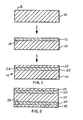
- the present invention is directed to a process for forming a composite 16.
- an alloy 10 comprising a first alloy component of about .5 to 12% aluminum and the matrix selected from a material of the group consisting of copper, iron or nickel is provided.
- the alloy 10 is heated in an oxygen-rich atmosphere to form a material oxide-rich layer 12 on a surface 18 of the alloy 10.
- the alloy 10 is heated in a reducing atmosphere to reduce the material oxide-rich layer 12 and form an aluminum oxide layer 20 on the surface of the alloy and a Material-rich layer 22 on a surface 24 of the aluminum oxide layer.
- the preferred alloy for use in the embodiments of the present invention is a copper base alloy containing from about .5 to 12% aluminum and the balance copper.
- the alloy contains from 2 to 10% aluminum, 0.001 to 6% silicon and if desired, a dispersion forming element selected from the group consisting of iron up to 4.5%, chromium up to 1%, zirconium up to 0.5%, cobalt up to 1% and mixtures of these grain refining elements and.the balance copper.
- CDA alloy C6381 as described in U.S. Patent Nos. 3,341,369 and 3,475,227 to Caule et al., containing 2.5 to 3.1% aluminum, 1.5 to 2.1% silicon, and the balance copper is useful as a substrate for this invention. Impurities may be present which do not prevent bonding in a desired environment.
- the present invention is not restricted to applications of alloy C6381 but includes the broad field of metals or alloys which have the ability to form a conductor layer separated by a continuous refractory oxide layer.
- alloy C6381 includes the broad field of metals or alloys which have the ability to form a conductor layer separated by a continuous refractory oxide layer.
- other metal alloys such as nickel base and iron base alloys are disclosed in U.S. Patent Nos. 3,698,964, 3,730,779 and 3,810,754.
- Alloy C6381 is particularly suitable for this invention because it is a commercial alloy which forms the desired composite when processed as described herein.
- the metal or alloy substrate may also include composite metals in which either the conductor layer or metal or alloy substrate is clad upon another metal by any conventional technique. This other metal may be another copper alloy or any other metal whose bulk properties are desired for a specific application.
- the process disclosed herein begins with preferably cleaning the selected alloy from any impurities in accordance with any desired technique such as for example, the cleaning process taught in U.S. Patent No. 4,361,445 to Pryor et al.
- the latter cleaning process begins with immersing the article to be cleaned in a stirred aqueous alkaline solution, as of sodium, potassium'or lithium hydroxide, having a pH above 10, for at least 2 seconds at a temperature between about 40°C and the boiling point. After draining and rinsing the article with water, it is submerged in a stirred aqueous solution of ferric sulfate or similar ferric salt of a mineral acid having a concentration of about 0.5 to 3.0 N.
- the material is submerged in the ferric sulfate for about 5 to 60 seconds at a temperature of about 25° to 95°C and preferably 60° to.90°C.
- Each step of the process should be followed by draining the solution from the article or subjecting it to blowing with airstreams and removing the residual solution by rinsing with water.
- the particular cleaning technique for removing the outer film on the surface of the alloy is not a part of the present invention and, therefore, any other desired cleaning technique may be used in place of the techniques set out hereinabove.
- the alloy is next annealed in an oxidizing environment, such as air, at a temperature of below about 500°C for a period of less than about 10 hours.
- the oxidizing atmosphere may be in the range of 0.1% to 100% oxygen but is preferably in the range of 1% to 25% oxygen: Further, the preferred temperature range for the annealing is between about 200° and 350°C at a preferred time of about 1 to 2 hours.
- a copper-rich layer 12 which is primarily copper oxide but may include other material such as copper aluminate.
- This copper oxide is a combination of cupric oxide and cuprous oxide although for purposes of this invention, they are collectiyely considered to be copper oxide.
- the thickness of the copper-rich layer is determined according to the desired thickness of the final copper-rich conductor layer 22 described hereinbelow.
- the copper alloy with the copper oxide-rich layer is now heated in a reducing atmosphere to reduce the copper oxide layer 12 and to form an aluminum oxide layer 20 on the surface 18 of the alloy and a copper-rich conductor layer 22 on the aluminum oxide layer 20.
- the alloy is subjected to a reducing atmosphere at a temperature of between approximately 500° to 850°C and optimally in the preferred range of from about 600° to 800°C.
- the time of holding the alloy at this elevated temperature should be for practical purposes less than 2 days, although longer heating times may be utilized if desired.
- the optimum heating time is from about 1 hour to 10 hours.
- the annealing is preferably performed in a wet reducing atmosphere of approximately 96% N 2 + 4% H 2 . Since the temperature is approximately 600° to 800°C, the copper oxide is in an unstable condition and cannot stay in the same state or form more copper oxide. Therefore, the copper oxide begins to reduce into a layer of substantially copper oxide plus pure copper. Simultaneous with this reaction, oxygen from the environment is able to diffuse through the copper oxide and copper layer and interact with the substrate to form a layer 20 of aluminum oxide. The oxygen primarily interacts with the aluminum because the oxygen potential or thermodynamics of the reaction is not favorable for the formation of copper oxide. As the process continues, the top layer 22 becomes copper-rich to an extent that it is a good electrical conductor while the aluminum oxide layer 20 becomes thick enough to be an electrical insulator. This 0 thickness is thought to be more than 100 A although it may be thinner if desired.
- the composite 16 of a copper alloy substrate 10 having an aluminum oxide insulator 20 sandwiched between a surface 18 of the substrate and a copper-rich conductor layer 22 has many potential uses for electronic devices.
- this article may provide an excellent alternative to the prior art printed circuit boards by simply etching a circuit into the conductor layer 22.
- a printed circuit board of this construction would have the advantages of being very durable, not being subject to stresses from thermal cycling, having high thermal conductivity characteristics and being relatively inexpensive to manufacture.
- the article 16 may also be adapted to provide a chip carrier which has the advantages as set forth above with regard to printed circuit. Other uses of this article, not enumerated herein, may be adapted to by direct application or slight modification of the herein described article.
- the process of the present invention has primarily been describing the formation of conductor and insulator layers on one surface of a substrate 10. However, as shown in Figure 2, it is also within the terms and scope of the present invention to form the same conductor and insulator layers on a second surface 26 of the substrate 10.
Landscapes
- Chemical & Material Sciences (AREA)
- Engineering & Computer Science (AREA)
- Inorganic Chemistry (AREA)
- Microelectronics & Electronic Packaging (AREA)
- Chemical Kinetics & Catalysis (AREA)
- Materials Engineering (AREA)
- Mechanical Engineering (AREA)
- Metallurgy (AREA)
- Organic Chemistry (AREA)
- Laminated Bodies (AREA)
Priority Applications (2)
| Application Number | Priority Date | Filing Date | Title |
|---|---|---|---|
| US06/467,616 US4500605A (en) | 1983-02-17 | 1983-02-17 | Electrical component forming process |
| EP84113849A EP0181416A1 (de) | 1983-02-17 | 1984-11-15 | Verfahren zur Herstellung eines elektrischen Bauelementes |
Applications Claiming Priority (2)
| Application Number | Priority Date | Filing Date | Title |
|---|---|---|---|
| US06/467,616 US4500605A (en) | 1983-02-17 | 1983-02-17 | Electrical component forming process |
| EP84113849A EP0181416A1 (de) | 1983-02-17 | 1984-11-15 | Verfahren zur Herstellung eines elektrischen Bauelementes |
Publications (1)
| Publication Number | Publication Date |
|---|---|
| EP0181416A1 true EP0181416A1 (de) | 1986-05-21 |
Family
ID=26092413
Family Applications (1)
| Application Number | Title | Priority Date | Filing Date |
|---|---|---|---|
| EP84113849A Withdrawn EP0181416A1 (de) | 1983-02-17 | 1984-11-15 | Verfahren zur Herstellung eines elektrischen Bauelementes |
Country Status (2)
| Country | Link |
|---|---|
| US (1) | US4500605A (de) |
| EP (1) | EP0181416A1 (de) |
Cited By (3)
| Publication number | Priority date | Publication date | Assignee | Title |
|---|---|---|---|---|
| EP0243709A1 (de) * | 1986-05-01 | 1987-11-04 | International Business Machines Corporation | Verfahren zur Herstellung eines Substrats für die gedruckte Schaltungstechnik |
| EP0366082A3 (de) * | 1988-10-28 | 1991-03-13 | Sumitomo Electric Industries, Ltd. | Träger für eine Halbleiteranordnung |
| EP0683243A3 (de) * | 1994-05-19 | 1996-12-04 | Wieland Werke Ag | Korrosionsbeständiges Rohr mit inneren Oxidschichten. |
Families Citing this family (24)
| Publication number | Priority date | Publication date | Assignee | Title |
|---|---|---|---|---|
| USRE32942E (en) * | 1983-10-06 | 1989-06-06 | Olin Corporation | Low thermal expansivity and high thermal conductivity substrate |
| US4736236A (en) * | 1984-03-08 | 1988-04-05 | Olin Corporation | Tape bonding material and structure for electronic circuit fabrication |
| US4805009A (en) * | 1985-03-11 | 1989-02-14 | Olin Corporation | Hermetically sealed semiconductor package |
| US4840654A (en) * | 1985-03-04 | 1989-06-20 | Olin Corporation | Method for making multi-layer and pin grid arrays |
| US4905074A (en) * | 1985-11-29 | 1990-02-27 | Olin Corporation | Interdiffusion resistant Fe-Ni alloys having improved glass sealing property |
| US4816216A (en) * | 1985-11-29 | 1989-03-28 | Olin Corporation | Interdiffusion resistant Fe--Ni alloys having improved glass sealing |
| US4771537A (en) * | 1985-12-20 | 1988-09-20 | Olin Corporation | Method of joining metallic components |
| US4743299A (en) * | 1986-03-12 | 1988-05-10 | Olin Corporation | Cermet substrate with spinel adhesion component |
| US4793967A (en) * | 1986-03-12 | 1988-12-27 | Olin Corporation | Cermet substrate with spinel adhesion component |
| US4767049A (en) * | 1986-05-19 | 1988-08-30 | Olin Corporation | Special surfaces for wire bonding |
| US4839716A (en) * | 1987-06-01 | 1989-06-13 | Olin Corporation | Semiconductor packaging |
| US4796083A (en) * | 1987-07-02 | 1989-01-03 | Olin Corporation | Semiconductor casing |
| US4888449A (en) * | 1988-01-04 | 1989-12-19 | Olin Corporation | Semiconductor package |
| US5213638A (en) * | 1990-07-27 | 1993-05-25 | Olin Corporation | Surface modified copper alloys |
| US5209787A (en) * | 1990-07-27 | 1993-05-11 | Olin Corporation | Surface modification of copper alloys |
| US5320689A (en) * | 1990-07-27 | 1994-06-14 | Olin Corporation | Surface modified copper alloys |
| US5096508A (en) * | 1990-07-27 | 1992-03-17 | Olin Corporation | Surface modified copper alloys |
| JPH05222471A (ja) * | 1991-12-16 | 1993-08-31 | Toshiba Corp | 装飾用銅鉄合金 |
| JP3493844B2 (ja) * | 1994-11-15 | 2004-02-03 | 住友電気工業株式会社 | 半導体基板材料とその製造方法及び該基板を用いた半導体装置 |
| JPH11509372A (ja) * | 1995-07-14 | 1999-08-17 | オリン コーポレイション | 金属ボール・グリッド電子パッケージ |
| US5965274A (en) * | 1997-11-13 | 1999-10-12 | Lockheed Martin Energy Research Corporation | Electronic circuits having NiAl and Ni3 Al substrates |
| US6283195B1 (en) | 1999-02-02 | 2001-09-04 | Metal Casting Technology, Incorporated | Passivated titanium aluminide tooling |
| DE102011119740A1 (de) | 2011-11-30 | 2013-06-06 | Emitec Gesellschaft Für Emissionstechnologie Mbh | Diffusionssperrschicht bei einer Abgasbehandlungseinheit |
| WO2019005989A1 (en) * | 2017-06-28 | 2019-01-03 | Arconic Inc. | PREPARATION METHODS FOR THE ADHESIVE BONDING OF 7XXX ALUMINUM ALLOYS AND PRODUCTS RELATED THERETO |
Citations (4)
| Publication number | Priority date | Publication date | Assignee | Title |
|---|---|---|---|---|
| US3914517A (en) * | 1971-02-23 | 1975-10-21 | Owens Illinois Inc | Method of forming a conductively coated crystalline glass article and product produced thereby |
| US3925579A (en) * | 1974-05-24 | 1975-12-09 | Armco Steel Corp | Method of coating low alloy steels |
| US4328048A (en) * | 1979-08-30 | 1982-05-04 | Murata Manufacturing Co., Ltd. | Method of forming copper conductor |
| EP0092020A2 (de) * | 1982-04-19 | 1983-10-26 | Olin Corporation | Zusammengesetzte Struktur insbesondere zur Benutzung als gedruckte Leiterplatte |
Family Cites Families (22)
| Publication number | Priority date | Publication date | Assignee | Title |
|---|---|---|---|---|
| US1851573A (en) * | 1932-03-29 | elsey | ||
| US1156170A (en) * | 1910-01-21 | 1915-10-12 | William Marshall Page | Alloy-surfaced wire and process of producing the same. |
| US3259526A (en) * | 1962-04-24 | 1966-07-05 | Honeywell Inc | Method of heat treatment |
| US3345218A (en) * | 1964-04-02 | 1967-10-03 | Owens Illinois Inc | Preoxidation of stainless steel for glass-to-metal sealing |
| US3341369A (en) * | 1965-03-03 | 1967-09-12 | Olin Mathieson | Copper base alloys and process for preparing same |
| US3475227A (en) * | 1966-10-04 | 1969-10-28 | Olin Mathieson | Copper base alloys and process for preparing same |
| US3546363A (en) * | 1967-01-11 | 1970-12-08 | Olin Corp | Composite glass-to-metal seal |
| US3618203A (en) * | 1969-08-25 | 1971-11-09 | Olin Mathieson | Method of making a glass or ceramic-to-composite metal seal |
| US3906125A (en) * | 1970-08-05 | 1975-09-16 | Scm Corp | Process of treating sheet steel |
| US3730779A (en) * | 1970-08-25 | 1973-05-01 | E Caule | Oxidation resistant iron base alloy |
| US3676292A (en) * | 1970-10-07 | 1972-07-11 | Olin Corp | Composites of glass-ceramic-to-metal,seals and method of making same |
| US3726987A (en) * | 1970-10-07 | 1973-04-10 | Olin Corp | Glass or ceramic-to-metal seals |
| US3826629A (en) * | 1970-10-07 | 1974-07-30 | Olin Corp | Products formed of glass or ceramicmetal composites |
| US3852148A (en) * | 1970-10-07 | 1974-12-03 | Olin Corp | Architectural products formed of glass or ceramic-to-metal composites |
| US3826627A (en) * | 1970-10-07 | 1974-07-30 | Olin Corp | Decorative composite articles |
| US3698964A (en) * | 1970-11-04 | 1972-10-17 | Olin Corp | Oxidation-resistant articles of an iron base alloy containing chromium and aluminum and/or silicon |
| US3837895A (en) * | 1972-05-18 | 1974-09-24 | Olin Corp | Organic resin-glass-metal composite |
| US3810754A (en) * | 1973-03-16 | 1974-05-14 | Olin Corp | Oxidation resistant nickel base alloys |
| US4149910A (en) * | 1975-05-27 | 1979-04-17 | Olin Corporation | Glass or ceramic-to-metal composites or seals involving iron base alloys |
| US4189331A (en) * | 1978-06-22 | 1980-02-19 | Canada Wire And Cable Limited | Oxidation resistant barrier coated copper based substrate and method for producing the same |
| US4361445A (en) * | 1978-09-13 | 1982-11-30 | Olin Corporation | Copper alloy cleaning process |
| US4229234A (en) * | 1978-12-29 | 1980-10-21 | Exxon Research & Engineering Co. | Passivated, particulate high Curie temperature magnetic alloys |
-
1983
- 1983-02-17 US US06/467,616 patent/US4500605A/en not_active Expired - Fee Related
-
1984
- 1984-11-15 EP EP84113849A patent/EP0181416A1/de not_active Withdrawn
Patent Citations (4)
| Publication number | Priority date | Publication date | Assignee | Title |
|---|---|---|---|---|
| US3914517A (en) * | 1971-02-23 | 1975-10-21 | Owens Illinois Inc | Method of forming a conductively coated crystalline glass article and product produced thereby |
| US3925579A (en) * | 1974-05-24 | 1975-12-09 | Armco Steel Corp | Method of coating low alloy steels |
| US4328048A (en) * | 1979-08-30 | 1982-05-04 | Murata Manufacturing Co., Ltd. | Method of forming copper conductor |
| EP0092020A2 (de) * | 1982-04-19 | 1983-10-26 | Olin Corporation | Zusammengesetzte Struktur insbesondere zur Benutzung als gedruckte Leiterplatte |
Cited By (3)
| Publication number | Priority date | Publication date | Assignee | Title |
|---|---|---|---|---|
| EP0243709A1 (de) * | 1986-05-01 | 1987-11-04 | International Business Machines Corporation | Verfahren zur Herstellung eines Substrats für die gedruckte Schaltungstechnik |
| EP0366082A3 (de) * | 1988-10-28 | 1991-03-13 | Sumitomo Electric Industries, Ltd. | Träger für eine Halbleiteranordnung |
| EP0683243A3 (de) * | 1994-05-19 | 1996-12-04 | Wieland Werke Ag | Korrosionsbeständiges Rohr mit inneren Oxidschichten. |
Also Published As
| Publication number | Publication date |
|---|---|
| US4500605A (en) | 1985-02-19 |
Similar Documents
| Publication | Publication Date | Title |
|---|---|---|
| US4500605A (en) | Electrical component forming process | |
| US4649083A (en) | Electrical component forming process | |
| US4491622A (en) | Composites of glass-ceramic to metal seals and method of making the same | |
| US5014159A (en) | Semiconductor package | |
| US4997722A (en) | Composition and method for improving adherence of copper foil to resinous substrates | |
| US4570337A (en) | Method of assembling a chip carrier | |
| US4997516A (en) | Method for improving adherence of copper foil to resinous substrates | |
| US4997698A (en) | Ceramic coated metal substrates for electronic applications | |
| KR101089201B1 (ko) | 도체 기재, 반도체 장치 및 이들의 제조 방법 | |
| US8021920B2 (en) | Method for producing a metal-ceramic substrate for electric circuits on modules | |
| US4851615A (en) | Printed circuit board | |
| EP0681322A2 (de) | Aus Keramik und Metall zusammengesetzte Substrate und damit konstruierte Schaltungsplatten | |
| US5716713A (en) | Stacked planar transformer | |
| EP0508195B1 (de) | Verfahren zur Herstellung mikroelektronischer Gehäuse mit Kupfersubstrat | |
| US6033764A (en) | Bumped substrate assembly | |
| US4853491A (en) | Chip carrier | |
| EP0139030B1 (de) | Gedruckte Schaltungsplatte | |
| EP0078582B1 (de) | Elektrische Schaltkreise | |
| JPH069290B2 (ja) | プリント回路用の金属基板 | |
| US4750262A (en) | Method of fabricating a printed circuitry substrate | |
| EP0092019A2 (de) | Halbleiterpackung | |
| EP0139029A1 (de) | Halbleiterpackung | |
| JPS61124560A (ja) | 複合材をつくる方法 | |
| JPH0528517B2 (de) | ||
| JP3663636B2 (ja) | プリント配線板とその製造方法 |
Legal Events
| Date | Code | Title | Description |
|---|---|---|---|
| PUAI | Public reference made under article 153(3) epc to a published international application that has entered the european phase |
Free format text: ORIGINAL CODE: 0009012 |
|
| AK | Designated contracting states |
Kind code of ref document: A1 Designated state(s): BE DE FR GB IT NL |
|
| STAA | Information on the status of an ep patent application or granted ep patent |
Free format text: STATUS: THE APPLICATION IS DEEMED TO BE WITHDRAWN |
|
| 18D | Application deemed to be withdrawn |
Effective date: 19870122 |
|
| RIN1 | Information on inventor provided before grant (corrected) |
Inventor name: BREEDIS, JOHN F. Inventor name: FISTER, JULIUS C. |