EP0181766A1 - Nichtinduktiver Schichtwiderstand für Hochspannung und Verfahren zu seiner Herstellung - Google Patents
Nichtinduktiver Schichtwiderstand für Hochspannung und Verfahren zu seiner Herstellung Download PDFInfo
- Publication number
- EP0181766A1 EP0181766A1 EP85308064A EP85308064A EP0181766A1 EP 0181766 A1 EP0181766 A1 EP 0181766A1 EP 85308064 A EP85308064 A EP 85308064A EP 85308064 A EP85308064 A EP 85308064A EP 0181766 A1 EP0181766 A1 EP 0181766A1
- Authority
- EP
- European Patent Office
- Prior art keywords
- line
- adjacent
- substrate
- film
- laser
- Prior art date
- Legal status (The legal status is an assumption and is not a legal conclusion. Google has not performed a legal analysis and makes no representation as to the accuracy of the status listed.)
- Granted
Links
- 238000004519 manufacturing process Methods 0.000 title claims abstract description 6
- 239000000758 substrate Substances 0.000 claims abstract description 42
- 239000000463 material Substances 0.000 claims abstract description 22
- 239000011248 coating agent Substances 0.000 claims abstract description 12
- 238000000576 coating method Methods 0.000 claims abstract description 12
- 230000000694 effects Effects 0.000 claims abstract description 5
- 238000000034 method Methods 0.000 claims description 13
- 239000011521 glass Substances 0.000 claims description 2
- 239000011159 matrix material Substances 0.000 claims description 2
- 229910044991 metal oxide Inorganic materials 0.000 claims description 2
- 150000004706 metal oxides Chemical class 0.000 claims description 2
- 239000010408 film Substances 0.000 description 25
- WYTGDNHDOZPMIW-RCBQFDQVSA-N alstonine Natural products C1=CC2=C3C=CC=CC3=NC2=C2N1C[C@H]1[C@H](C)OC=C(C(=O)OC)[C@H]1C2 WYTGDNHDOZPMIW-RCBQFDQVSA-N 0.000 description 9
- 238000012216 screening Methods 0.000 description 7
- 238000003698 laser cutting Methods 0.000 description 5
- 238000005538 encapsulation Methods 0.000 description 4
- PNEYBMLMFCGWSK-UHFFFAOYSA-N Alumina Chemical compound [O-2].[O-2].[O-2].[Al+3].[Al+3] PNEYBMLMFCGWSK-UHFFFAOYSA-N 0.000 description 3
- 230000015556 catabolic process Effects 0.000 description 3
- 230000001965 increasing effect Effects 0.000 description 3
- 238000005520 cutting process Methods 0.000 description 2
- 229930091051 Arenine Natural products 0.000 description 1
- 239000000919 ceramic Substances 0.000 description 1
- 230000007423 decrease Effects 0.000 description 1
- 230000003247 decreasing effect Effects 0.000 description 1
- 239000012777 electrically insulating material Substances 0.000 description 1
- 230000001939 inductive effect Effects 0.000 description 1
- 239000011810 insulating material Substances 0.000 description 1
- 238000002955 isolation Methods 0.000 description 1
- 230000000873 masking effect Effects 0.000 description 1
- 230000000750 progressive effect Effects 0.000 description 1
- 239000010409 thin film Substances 0.000 description 1
- 238000009834 vaporization Methods 0.000 description 1
- 230000008016 vaporization Effects 0.000 description 1
Images

Classifications
-
- H—ELECTRICITY
- H01—ELECTRIC ELEMENTS
- H01C—RESISTORS
- H01C7/00—Non-adjustable resistors formed as one or more layers or coatings; Non-adjustable resistors made from powdered conducting material or powdered semi-conducting material with or without insulating material
- H01C7/22—Elongated resistive element being bent or curved, e.g. sinusoidal, helical
-
- Y—GENERAL TAGGING OF NEW TECHNOLOGICAL DEVELOPMENTS; GENERAL TAGGING OF CROSS-SECTIONAL TECHNOLOGIES SPANNING OVER SEVERAL SECTIONS OF THE IPC; TECHNICAL SUBJECTS COVERED BY FORMER USPC CROSS-REFERENCE ART COLLECTIONS [XRACs] AND DIGESTS
- Y10—TECHNICAL SUBJECTS COVERED BY FORMER USPC
- Y10T—TECHNICAL SUBJECTS COVERED BY FORMER US CLASSIFICATION
- Y10T29/00—Metal working
- Y10T29/49—Method of mechanical manufacture
- Y10T29/49002—Electrical device making
- Y10T29/49082—Resistor making
Definitions
- Noninductive film-type resistors made by the silk screening of thick-film resistive material onto substrates are known.
- US-A-3,858,147 and corresponding GB-A-1,482,164 describe silk screening a serpentine pattern of such material onto a cylindrical substrate.
- GB-A-1,314,388, describes the silk screening of resistive material in a zigzag pattern onto a cylindrical substrate.
- serpentine resistors by cutting grooves with a laser in resistive material deposited by silk screening. This is often done, for example, relative to thick-film flat resistors, on which the films are fused before they are removed with the laser beam.
- US-A-4,159,459 describes a thin-film cylindrical resistor that is laser cut into a serpentine noninductive pattern.
- a method of making a high-voltage, noninductive film-type resistor comprises providing on an insulating substrate, a coating of resistive material, and selectively removing the coating using a laser beam to leave a zigzag line of the resistive material on the substrate, adjacent portions of the zigzag line converging towards each other at an angle sufficiently small that, in use, there is a major inductance cancellation effect between current flowing in them.
- the coating is selectively removed by removing the resistive material from a series of parallel adjacent regions of different length to provide the zig-zag line with a stepped edge.
- a high-voltage film type resistor comprises
- the resulting high-voltage resistor can be and is much more compact than is a conventional noninductive film-type resistor having the same voltage capability. Furthermore, and very importantly, the amount of laser time required to manufacture each high-voltage resistor is small in comparison to what would be the case if the laser-cut pattern were serpentine instead of zigzag.
- the pattern is generated by making parallel laser cuts in stepped relationship to each other.
- the adjacent cuts are progressively longer and longer and/or shorter and __ shorter. There are, therefore, stepped side portions of the resistive line.
- the regions between adjacent zigs and zags are generally triangular, they being either isosceles or right (or other) triangles, as shown in the drawings.
- the resulting zigzag line of resistive film can be, and preferably is, substantially less wide than is practical when a patterned film is printed by silk screening.
- the line width has a preferred range of from about one-half of the gap to about the full width of the gap between adjacent apex regions of the zigzag line.
- the maximum compactness of the resistor is achieved when line width is one-half of the gap width.
- the word "serpentine” is used not in its broader sense but instead narrowly, to denote resistive film patterns wherein adjacent lengths or arms of the resistive line are parallel to each other except at their apexes.
- zigzag is used to denote angular, not parallel, relationships between adjacent lengths or arms called zigs and zags of the resistive line.
- line denotes the strip of resistive film through which the current flows.
- the word "gap” denotes the spacing between adjacent apexes of the zigzag line.
- the present film-type resistor may be flat, cylindrical, or of any other shape such as ellipsoidal. For purposes of simplicity of illustration, the present resistors are shown flat. Whether flat or cylindrical or other each resistor has end terminations, encapsulation means, etc. As typical examples of end terminations and encapsulation, reference is made to elements 23, 24, 26, 27, and 28 of US-A-3,858,147, which patent is hereby incorporated by reference herein. This specification relates to a cylindrical resistor, but the same terminations and encapsulation could be employed for flat resistors, except that the termination films 23 and 24 ( Figure 8 of US-A-3,858,147) and end caps 26 (Fig. 9 thereof) are flat instead of cylindrical. Any suitable termination and encapsulation means known in the art may be employed.
- the first steps in the method are to provide a substrate 10 of desired size and shape and to coat such substrate with a film of resistive material.
- the illustrated substrate 10 is rectangular, and is formed of electrically insulating material.
- such insulating material is a suitable heat-resistant ceramic, such as aluminium oxide.
- the resistive material is a thick film and is preferably provided on the substrate 10 by silk screening.
- the film is applied to one side of the substrate 10, for example by the apparatus and method described in US-A-3,880,609, the disclosure of which is incorporated by reference herein.
- the film which is preferably a complex oxide resistive material consisting of electrically conductive complex metal oxides in a glass matrix, is fired and fused as stated in US-A-3,880,609.
- the coated substrate is placed in a suitable laser apparatus.
- a laser is indicated schematically in US-A-3388461 the disclosure of which is hereby incorporated by reference herein.
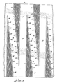
- the laser is employed to remove from the coated substrate all of the coating except that present along a zigzag line of resistive film.
- Such line is indicated generally by the number 11.
- Line 11 is formed by removing, from between adjacent zigs and zags of the zigzag line, progressively longer and longer, and then shorter and shorter, strips or paths of cut regions created by vaporization of the fused resistive film where struck by the laser beam.
- a first laser cut is shown at 12 and is relatively short.
- the next laser cut, numbered 13, is much longer, and subsequent laser cuts 14, 15, 16, and 17 are all progressively longer.
- progressively shorter and shorter laser cuts 18, 19, 20, 21 and 22 are made. Each such cut extends to the lower edge of substrate 10.
- each triangle or pyramid is relatively wide at the base, that is to say at the lower edge of the substrate, and tapers or converges in stepped manner, along the equal sides of the isosceles triangle away from such base toward the upper edge until the narrowest point, in this case the inner end of laser cut 17, is reached.
- the triangle is symmetrical about its central axis, namely the axis of laser cut 17.
- the outermost laser cuts 12 and 22 have the same lengths, as do the next cuts 13 and 21, the next 14 and 20, etc.
- next laser cut 23 is generally opposite cut 22 but extends from the upper edge of substrate 10 instead of the lower edge thereof.
- Progressively longer and longer laser cuts are then made from such upper edge to form the cut regions 24 through 28, following which progressively shorter laser cuts are made from such upper edge to form the cut regions 29-33.
- the triangle or pyramid formed by laser cuts 23-33 is identical to that formed by laser cuts 12-22, except that it extends from the opposite edge and in the opposite direction.
- Additional laser cuts are made at other portions of the substrate to create as many zigs and zags of line 11 as desired. Such additional laser cuts correspond, respectively, to cuts 12-22 and to cuts 23-33, being therefore so numbered.
- the described triangle or pyramids of laser-cut regions are interleaved, as shown, to define zigs and zags lla, llb, llc, etc.
- the zigs and zags of line 11 meet at apex regions 29a, 30a, 31a, etc. Such apexes are between the longest cuts 17, 28, etc., and the opposed edges of substrate 10. _
- the spacing between zig lla and zag 11b decreases progressively, in stepped relationship, as apex 29a for example is approached.
- the inner ends of laser cuts 26 and 30 combine with the laser cuts therebetween to create a space which is much less than gap G.
- this is not harmful because the voltage drop or tension between those line regions adjacent the inner ends of cuts 26 and 30 is greatly less than is the voltage drop across gap G.
- the present compact resistor has a highly desirable low-inductance characteristic. This is because the angle between each zig and the adjacent zag is sufficiently small that the current flowing in opposite directions therethrough will effectively cancel inductance.
- each laser cut 12-16 and 18-22 (for example) would have to be as long as is the illustrated centre cut 17. Instead, the outer cuts 12 and 22, for example, are only a small fraction of the length of such centre cut 17.
- the width of the resistive film line 11 at regions other than the apexes be in a range of from about one-half gap G to about one gap G (that is to say that, at the high end of the range, line width about equals gap width).
- the width of line 11 is (except at the apexes) about 60% of gap G.
- line width is slightly greater than the width of gap G' of that figure. For maximum compactness of the substrate, line width is caused to be 50% of gap width.
- the adjacent ends of oppositely-directed laser cuts terminate along lines parallel to the axis of the resistor.
- the inner ends of lines 18 and 24 (or 19 and 25, etc) end at the same imaginary horizontal line.
- both side edges of the line “step” horizontally at substantially the same points, which means that the entire line is stepped as shown. The result is that the line has a substantially uniform width.
- the altitudes of the pyramids or triangles be perpendicular to the edges of the substrate.
- all of the laser cuts may be along the same helix, the axis of which is coincident with the axis of the substrate.
- the substrate is then rotated about its axis, and the laser beam is turned on and off in such programmed manner as to generate the desired substantially triangular or pyramidal regions where the resistive film is totally removed. There is also thus generated a line of exposed substrate that corresponds to gap 13 shown in Figure 1 of US-A-3,858,147).
- the laser is a YAG laser apparatus having a focused beam.
- the diameter of the beam is, for example, 1.5 mils (40 ⁇ m).
- the machine will shift the beam laterally by a certain increment, after making each of the parallel cuts shown in Figure 1, not necessarily by an physical movement of any table or support or beam generator, but instead optically.
- the lateral beam shifting may be effected by masking, by movement of a table, etc.
- Other diameter beams may be employed, for example, one having a diameter of 2 mils (50 ⁇ m).
- each such increment is 0.4 mil (10 ⁇ m) .
- the machine is caused to shift three times before the making of each cut.
- a 0.3 mil( ⁇ 10 ⁇ m) overlap between adjacent cuts to assure that there will be complete removal of resistive film and thus maximized insurance against any breakdown.
- Typical overlap regions are shown at 32a at upper portions of Figure 1.
- a highly efficient, compact, stable, non-inductive resistor pattern is provided.
- the resistive film is cut away by successive passes of the laser to form the V-shaped or zigzag resistance path.
- the laser cuts a 1.5 mil (40 ⁇ m) wide path in the Y direction, that is to say generally perpendicular to the horizontal edge of the illustrated substrate, and there are stop and start points relative to laser operation and which are appropriate to provide a stepped, sloped edge as each cut is indexed in the X direction, that is to say generally horizontally.
- Optimum high-voltage capability is permitted because the stress between adjacent line portions is graduated, this being contrasted to what would be the case if the laser cuts were parallel and the same length, as would be the case if the pattern were serpentine.
- each line portion that is to say each zig 11a or llc, and each zag llb, is determined by the heights of the laser cuts (lengths thereof).
- each laser cut may be relatively short, or it may have a length at least 50, 100, or even more times the width of the cut (diameter of the laser beam).
- Figure 3 there is shown (in a scale which is intermediate that of Figures 1 and 2) a resistor in which the triangles are right triangles instead of isosceles. (There may also be forms wherein the triangles are neither isosceles nor right). Except as specifically stated, the embodiment of Figure 3 is identical to that of Figures 1 and 2.
- the right-triangle embodiment is preferred.
- the showing of Figure 3 is preferred except that for increased resistor compactness the width of the line is preferably caused to be about one-half the gap G' shown in Figure 3 (instead of being slightly larger as shown).
- all embodiments achieve stable, practical, high-precision, compact, high-voltage resistors that are extremely desirable for many applications.
- the resistive coating need not necessarily cover the entire substrate before laser cutting commences.
- a longitudinal gap may be left unprinted during the silk screening.
Landscapes
- Engineering & Computer Science (AREA)
- Microelectronics & Electronic Packaging (AREA)
- Physics & Mathematics (AREA)
- Electromagnetism (AREA)
- Apparatuses And Processes For Manufacturing Resistors (AREA)
- Non-Adjustable Resistors (AREA)
Priority Applications (1)
| Application Number | Priority Date | Filing Date | Title |
|---|---|---|---|
| AT85308064T ATE34635T1 (de) | 1984-11-14 | 1985-11-06 | Nichtinduktiver schichtwiderstand fuer hochspannung und verfahren zu seiner herstellung. |
Applications Claiming Priority (2)
| Application Number | Priority Date | Filing Date | Title |
|---|---|---|---|
| US671333 | 1984-11-14 | ||
| US06/671,333 US4670734A (en) | 1984-11-14 | 1984-11-14 | Method of making a compact, high-voltage, noninductive, film-type resistor |
Publications (2)
| Publication Number | Publication Date |
|---|---|
| EP0181766A1 true EP0181766A1 (de) | 1986-05-21 |
| EP0181766B1 EP0181766B1 (de) | 1988-05-25 |
Family
ID=24694082
Family Applications (1)
| Application Number | Title | Priority Date | Filing Date |
|---|---|---|---|
| EP85308064A Expired EP0181766B1 (de) | 1984-11-14 | 1985-11-06 | Nichtinduktiver Schichtwiderstand für Hochspannung und Verfahren zu seiner Herstellung |
Country Status (5)
| Country | Link |
|---|---|
| US (1) | US4670734A (de) |
| EP (1) | EP0181766B1 (de) |
| JP (1) | JPH0630294B2 (de) |
| AT (1) | ATE34635T1 (de) |
| DE (1) | DE3562959D1 (de) |
Families Citing this family (16)
| Publication number | Priority date | Publication date | Assignee | Title |
|---|---|---|---|---|
| DE3710286A1 (de) * | 1987-03-28 | 1988-10-06 | Preh Elektro Feinmechanik | Weg- bzw. positionsgeber |
| US4881057A (en) * | 1987-09-28 | 1989-11-14 | Ranco Incorporated | Temperature sensing apparatus and method of making same |
| US5133732A (en) | 1987-10-19 | 1992-07-28 | Medtronic, Inc. | Intravascular stent |
| US5360140A (en) * | 1988-12-16 | 1994-11-01 | The Cornelius Company | Low cost control circuit for sensing the operation of an electrically operable device |
| US6344053B1 (en) | 1993-12-22 | 2002-02-05 | Medtronic Ave, Inc. | Endovascular support device and method |
| US5119538A (en) * | 1990-08-10 | 1992-06-09 | Ranco Incorporated Of Delaware | Method of making a temperature sensor |
| US5231372A (en) * | 1991-10-09 | 1993-07-27 | Caddock Electronics, Inc. | Method of manufacturing high-voltage and/or high-power thick-film screen-printed cylindrical resistors having small sizes, low voltage coefficients, and low inductance, and resistor thus manufactured |
| US5922514A (en) | 1997-09-17 | 1999-07-13 | Dale Electronics, Inc. | Thick film low value high frequency inductor, and method of making the same |
| US6967312B2 (en) * | 2000-07-19 | 2005-11-22 | Ibiden Co., Ltd. | Semiconductor manufacturing/testing ceramic heater, production method for the ceramic heater and production system for the ceramic heater |
| EP1255284A1 (de) * | 2000-07-19 | 2002-11-06 | Ibiden Co., Ltd. | Keramischer heizkörper für die bearbeitung bzw. das testen von halbleitern |
| US6452477B1 (en) * | 2000-09-06 | 2002-09-17 | Marconi Medical Systems, Inc. | High voltage low inductance circuit protection resistor |
| US20040035846A1 (en) * | 2000-09-13 | 2004-02-26 | Yasuji Hiramatsu | Ceramic heater for semiconductor manufacturing and inspecting equipment |
| SG119230A1 (en) * | 2004-07-29 | 2006-02-28 | Micron Technology Inc | Interposer including at least one passive element at least partially defined by a recess formed therein method of manufacture system including same and wafer-scale interposer |
| JP5179155B2 (ja) * | 2007-12-07 | 2013-04-10 | 太陽社電気株式会社 | チップ抵抗器 |
| US10575973B2 (en) | 2018-04-11 | 2020-03-03 | Abbott Cardiovascular Systems Inc. | Intravascular stent having high fatigue performance |
| US10297373B1 (en) * | 2018-04-19 | 2019-05-21 | Littelfuse, Inc. | Jelly roll-type positive temperature coefficient device |
Citations (2)
| Publication number | Priority date | Publication date | Assignee | Title |
|---|---|---|---|---|
| FR2477829A1 (fr) * | 1980-03-07 | 1981-09-11 | Labo Electronique Physique | Realisation d'un circuit hyperfrequence en couches serigraphiees |
| DE3021288A1 (de) * | 1980-06-06 | 1981-12-24 | Licentia Patent-Verwaltungs-Gmbh, 6000 Frankfurt | Abgleichbarer schichtwiderstand, insbesondere fuer hochspannungsanwendung |
Family Cites Families (33)
| Publication number | Priority date | Publication date | Assignee | Title |
|---|---|---|---|---|
| US1318030A (en) * | 1919-10-07 | John thomson | ||
| US1068907A (en) * | 1910-12-10 | 1913-07-29 | Westinghouse Electric & Mfg Co | Resister. |
| US1321682A (en) * | 1918-10-07 | 1919-11-11 | John Thomson | Zigzag carbon electric resister. |
| US2056928A (en) * | 1930-05-31 | 1936-10-06 | Resistelite Corp | Method of making resistance units |
| US1975410A (en) * | 1931-12-12 | 1934-10-02 | Pittsburgh Res Corp | Electric heating furnace |
| US2680184A (en) * | 1951-02-07 | 1954-06-01 | Duncan B Cox | Method for severing or slitting metal foil |
| US2736852A (en) * | 1955-01-10 | 1956-02-28 | Eldred C Nelson | Automatic digital motor control system for machine tools |
| US2838427A (en) * | 1956-10-23 | 1958-06-10 | Int Resistance Co | Method and apparatus for flame spiralling |
| US3074042A (en) * | 1959-11-25 | 1963-01-15 | Gen Electric | Low-inductance resistor |
| US3289139A (en) * | 1964-02-24 | 1966-11-29 | Dale Electronics | Film resistance unit |
| US3388461A (en) * | 1965-01-26 | 1968-06-18 | Sperry Rand Corp | Precision electrical component adjustment method |
| US3293587A (en) * | 1965-10-20 | 1966-12-20 | Sprague Electric Co | Electrical resistor and the like |
| US3530573A (en) * | 1967-02-24 | 1970-09-29 | Sprague Electric Co | Machined circuit element process |
| NL6707448A (de) * | 1967-05-30 | 1968-12-02 | ||
| US3486221A (en) * | 1967-06-14 | 1969-12-30 | Sprague Electric Co | High energy beam trimming of electrical components |
| US3539309A (en) * | 1967-07-11 | 1970-11-10 | Sprague Electric Co | Circuit component machining |
| US3699649A (en) * | 1969-11-05 | 1972-10-24 | Donald A Mcwilliams | Method of and apparatus for regulating the resistance of film resistors |
| US3675317A (en) * | 1970-05-13 | 1972-07-11 | Welwya Canada Ltd | Method for spiralling electrical resistors |
| GB1314388A (en) * | 1970-07-13 | 1973-04-18 | Fasterr Transformers Ltd | Resistors |
| DE2036663B2 (de) * | 1970-07-23 | 1973-08-02 | Siemens AG, 1000 Berlin u 8000 München | Verfahren zur herstellung belagfreier laengsrandstreifen auf unterlagen, welche mit einem elektrisch leitfaehigen belag versehen sind |
| US3683213A (en) * | 1971-03-09 | 1972-08-08 | Statek Corp | Microresonator of tuning fork configuration |
| JPS4825076U (de) * | 1971-07-31 | 1973-03-24 | ||
| US3758745A (en) * | 1971-09-07 | 1973-09-11 | Microsystems Int Ltd | Substrate positioned determination structure and method |
| US3845443A (en) * | 1972-06-14 | 1974-10-29 | Bailey Meter Co | Thin film resistance thermometer |
| US3858147A (en) * | 1972-12-14 | 1974-12-31 | R Caddock | Non-inductive film-type cylindrical resistor |
| US3880609A (en) * | 1972-12-14 | 1975-04-29 | Richard E Caddock | Method and apparatus for manufacturing cylindrical resistors by thick-film silk-screening |
| JPS5043834U (de) * | 1973-08-20 | 1975-05-02 | ||
| US3881162A (en) * | 1974-04-01 | 1975-04-29 | Richard E Caddock | Film-type cylindrical resistor and method of manufacturing |
| JPS5286150A (en) * | 1976-01-12 | 1977-07-18 | Hitachi Ltd | Method of forming pattern for thinnfilm resistors |
| US4072921A (en) * | 1976-04-27 | 1978-02-07 | Amf Incorporated | Low inductance precision resistor deposited on an adhesive backing and wound on a bobbin |
| US4132971A (en) * | 1977-02-28 | 1979-01-02 | Caddock Jr Richard E | Noninductive film-type cylindrical resistor and method of making it |
| US4159459A (en) * | 1977-06-23 | 1979-06-26 | Angstrohm Precision, Inc. | Non-inductive cylindrical thin film resistor |
| JPS54101339U (de) * | 1977-12-27 | 1979-07-17 |
-
1984
- 1984-11-14 US US06/671,333 patent/US4670734A/en not_active Expired - Lifetime
-
1985
- 1985-11-06 DE DE8585308064T patent/DE3562959D1/de not_active Expired
- 1985-11-06 AT AT85308064T patent/ATE34635T1/de not_active IP Right Cessation
- 1985-11-06 EP EP85308064A patent/EP0181766B1/de not_active Expired
- 1985-11-11 JP JP60252581A patent/JPH0630294B2/ja not_active Expired - Fee Related
Patent Citations (2)
| Publication number | Priority date | Publication date | Assignee | Title |
|---|---|---|---|---|
| FR2477829A1 (fr) * | 1980-03-07 | 1981-09-11 | Labo Electronique Physique | Realisation d'un circuit hyperfrequence en couches serigraphiees |
| DE3021288A1 (de) * | 1980-06-06 | 1981-12-24 | Licentia Patent-Verwaltungs-Gmbh, 6000 Frankfurt | Abgleichbarer schichtwiderstand, insbesondere fuer hochspannungsanwendung |
Non-Patent Citations (1)
| Title |
|---|
| 23RD ELECTRONIC COMPONENTS CONFERENCE, 14th-16th May 1973, pages 38-44, Washington, D.C., US; L. GROTH et al.: "Laser trimming thin film precision resistor networks with an automated system" * |
Also Published As
| Publication number | Publication date |
|---|---|
| US4670734A (en) | 1987-06-02 |
| DE3562959D1 (en) | 1988-06-30 |
| JPS61136202A (ja) | 1986-06-24 |
| JPH0630294B2 (ja) | 1994-04-20 |
| EP0181766B1 (de) | 1988-05-25 |
| ATE34635T1 (de) | 1988-06-15 |
Similar Documents
| Publication | Publication Date | Title |
|---|---|---|
| EP0181766B1 (de) | Nichtinduktiver Schichtwiderstand für Hochspannung und Verfahren zu seiner Herstellung | |
| US4453199A (en) | Low cost thin film capacitor | |
| US5548268A (en) | Fine-line thick film resistors and resistor networks and method of making same | |
| DE69833193T2 (de) | Verfahren zur herstellung mehrerer elektronischer bauteile | |
| DE112006002516B4 (de) | Chip-Widertand und Befestigungsstruktur für einen Chip-Widerstand | |
| DE69125307T2 (de) | Kleinstsicherung für niedere Stromstärke | |
| DE3720189C1 (de) | Taupunkt-Sensor | |
| US4463338A (en) | Electrical network and method for producing the same | |
| EP0033739B1 (de) | Verfahren zum herstellen eines widerstandes | |
| DE112006002517T5 (de) | Chip-Widerstand | |
| US6724295B2 (en) | Chip resistor with upper electrode having nonuniform thickness and method of making the resistor | |
| JPH10289803A (ja) | 抵抗器およびその製造方法 | |
| DE19848832B4 (de) | Thermistoren und Verfahren zum Einstellen und Erzeugen von Thermistoren | |
| EP0242461A1 (de) | Monolitischer elektrischer Miniatur-Kondensator | |
| EP0536895B1 (de) | Durch Siebdruck hergestellter zylindrischer Widerstand und sein Herstellungsverfahren | |
| US4794367A (en) | Circuit arrangement | |
| KR20030088496A (ko) | 다련 칩 저항기의 제조방법 | |
| US4630025A (en) | Small-sized precision high-voltage resistor in thick-film technology | |
| US5639391A (en) | Laser formed electrical component and method for making the same | |
| DE2700946C2 (de) | Abgleichbarer Schichtwiderstand mit möglichst geringer Induktivität | |
| DE3040930C2 (de) | Verfahren zur serienmäßigen Herstellung von elektrischen Bauelementen oder Netzwerken in Chip-Bauweise | |
| DE3117957A1 (de) | Verfahren zur herstellung eines schichtwiderstandes und nach diesem verfahren hergestellter schichtwiderstand | |
| JP3476849B2 (ja) | ヒユーズ抵抗器およびその製造方法 | |
| JPH0636675A (ja) | ヒユーズ抵抗器およびその製造方法 | |
| JPH0347289Y2 (de) |
Legal Events
| Date | Code | Title | Description |
|---|---|---|---|
| PUAI | Public reference made under article 153(3) epc to a published international application that has entered the european phase |
Free format text: ORIGINAL CODE: 0009012 |
|
| AK | Designated contracting states |
Kind code of ref document: A1 Designated state(s): AT BE CH DE FR GB IT LI LU NL SE |
|
| 17P | Request for examination filed |
Effective date: 19860819 |
|
| 17Q | First examination report despatched |
Effective date: 19870811 |
|
| GRAA | (expected) grant |
Free format text: ORIGINAL CODE: 0009210 |
|
| AK | Designated contracting states |
Kind code of ref document: B1 Designated state(s): AT BE CH DE FR GB IT LI LU NL SE |
|
| REF | Corresponds to: |
Ref document number: 34635 Country of ref document: AT Date of ref document: 19880615 Kind code of ref document: T |
|
| REF | Corresponds to: |
Ref document number: 3562959 Country of ref document: DE Date of ref document: 19880630 |
|
| ITF | It: translation for a ep patent filed | ||
| ET | Fr: translation filed | ||
| PLBE | No opposition filed within time limit |
Free format text: ORIGINAL CODE: 0009261 |
|
| STAA | Information on the status of an ep patent application or granted ep patent |
Free format text: STATUS: NO OPPOSITION FILED WITHIN TIME LIMIT |
|
| 26N | No opposition filed | ||
| ITTA | It: last paid annual fee | ||
| PGFP | Annual fee paid to national office [announced via postgrant information from national office to epo] |
Ref country code: FR Payment date: 19931011 Year of fee payment: 9 |
|
| PGFP | Annual fee paid to national office [announced via postgrant information from national office to epo] |
Ref country code: CH Payment date: 19931014 Year of fee payment: 9 |
|
| PGFP | Annual fee paid to national office [announced via postgrant information from national office to epo] |
Ref country code: LU Payment date: 19931015 Year of fee payment: 9 |
|
| PGFP | Annual fee paid to national office [announced via postgrant information from national office to epo] |
Ref country code: AT Payment date: 19931018 Year of fee payment: 9 |
|
| PGFP | Annual fee paid to national office [announced via postgrant information from national office to epo] |
Ref country code: SE Payment date: 19931020 Year of fee payment: 9 |
|
| PGFP | Annual fee paid to national office [announced via postgrant information from national office to epo] |
Ref country code: DE Payment date: 19931022 Year of fee payment: 9 |
|
| PGFP | Annual fee paid to national office [announced via postgrant information from national office to epo] |
Ref country code: BE Payment date: 19931025 Year of fee payment: 9 |
|
| PGFP | Annual fee paid to national office [announced via postgrant information from national office to epo] |
Ref country code: GB Payment date: 19931028 Year of fee payment: 9 |
|
| PGFP | Annual fee paid to national office [announced via postgrant information from national office to epo] |
Ref country code: NL Payment date: 19931130 Year of fee payment: 9 |
|
| EPTA | Lu: last paid annual fee | ||
| PG25 | Lapsed in a contracting state [announced via postgrant information from national office to epo] |
Ref country code: LU Free format text: LAPSE BECAUSE OF NON-PAYMENT OF DUE FEES Effective date: 19941106 Ref country code: GB Effective date: 19941106 Ref country code: AT Effective date: 19941106 |
|
| PG25 | Lapsed in a contracting state [announced via postgrant information from national office to epo] |
Ref country code: SE Effective date: 19941107 |
|
| PG25 | Lapsed in a contracting state [announced via postgrant information from national office to epo] |
Ref country code: LI Effective date: 19941130 Ref country code: CH Effective date: 19941130 Ref country code: BE Effective date: 19941130 |
|
| EAL | Se: european patent in force in sweden |
Ref document number: 85308064.6 |
|
| BERE | Be: lapsed |
Owner name: CADDOCK RICHARD E. Effective date: 19941130 |
|
| PG25 | Lapsed in a contracting state [announced via postgrant information from national office to epo] |
Ref country code: NL Effective date: 19950601 |
|
| GBPC | Gb: european patent ceased through non-payment of renewal fee |
Effective date: 19941106 |
|
| NLV4 | Nl: lapsed or anulled due to non-payment of the annual fee | ||
| PG25 | Lapsed in a contracting state [announced via postgrant information from national office to epo] |
Ref country code: FR Effective date: 19950731 |
|
| REG | Reference to a national code |
Ref country code: CH Ref legal event code: PL |
|
| PG25 | Lapsed in a contracting state [announced via postgrant information from national office to epo] |
Ref country code: DE Effective date: 19950801 |
|
| EUG | Se: european patent has lapsed |
Ref document number: 85308064.6 |
|
| REG | Reference to a national code |
Ref country code: FR Ref legal event code: ST |