EP0181801A1 - Oszillator sehr hoher Frequenz mit gyromagnetischen Resonatoren - Google Patents
Oszillator sehr hoher Frequenz mit gyromagnetischen Resonatoren Download PDFInfo
- Publication number
- EP0181801A1 EP0181801A1 EP85402047A EP85402047A EP0181801A1 EP 0181801 A1 EP0181801 A1 EP 0181801A1 EP 85402047 A EP85402047 A EP 85402047A EP 85402047 A EP85402047 A EP 85402047A EP 0181801 A1 EP0181801 A1 EP 0181801A1
- Authority
- EP
- European Patent Office
- Prior art keywords
- oscillator
- ball
- resonator
- yig
- transistor
- Prior art date
- Legal status (The legal status is an assumption and is not a legal conclusion. Google has not performed a legal analysis and makes no representation as to the accuracy of the status listed.)
- Granted
Links
- 230000005669 field effect Effects 0.000 claims abstract description 19
- 239000000463 material Substances 0.000 claims abstract description 4
- 239000002223 garnet Substances 0.000 claims description 8
- 239000004020 conductor Substances 0.000 claims description 6
- XEEYBQQBJWHFJM-UHFFFAOYSA-N iron Substances [Fe] XEEYBQQBJWHFJM-UHFFFAOYSA-N 0.000 claims description 2
- 229910052742 iron Inorganic materials 0.000 claims description 2
- MTRJKZUDDJZTLA-UHFFFAOYSA-N iron yttrium Chemical compound [Fe].[Y] MTRJKZUDDJZTLA-UHFFFAOYSA-N 0.000 claims description 2
- 239000000696 magnetic material Substances 0.000 claims 2
- 230000008878 coupling Effects 0.000 abstract description 4
- 238000010168 coupling process Methods 0.000 abstract description 4
- 238000005859 coupling reaction Methods 0.000 abstract description 4
- 230000010355 oscillation Effects 0.000 description 12
- 238000010586 diagram Methods 0.000 description 8
- CAWXEEYDBZRFPE-UHFFFAOYSA-N Hexazinone Chemical compound O=C1N(C)C(N(C)C)=NC(=O)N1C1CCCCC1 CAWXEEYDBZRFPE-UHFFFAOYSA-N 0.000 description 6
- 230000001939 inductive effect Effects 0.000 description 5
- 229910052727 yttrium Inorganic materials 0.000 description 5
- VWQVUPCCIRVNHF-UHFFFAOYSA-N yttrium atom Chemical compound [Y] VWQVUPCCIRVNHF-UHFFFAOYSA-N 0.000 description 5
- 238000006243 chemical reaction Methods 0.000 description 4
- 239000013078 crystal Substances 0.000 description 2
- 238000001228 spectrum Methods 0.000 description 2
- 239000011324 bead Substances 0.000 description 1
- 230000000295 complement effect Effects 0.000 description 1
- 230000003247 decreasing effect Effects 0.000 description 1
- 230000000694 effects Effects 0.000 description 1
- SBXWKPKGSPXIKG-UHFFFAOYSA-N gallium yttrium Chemical compound [Ga].[Y] SBXWKPKGSPXIKG-UHFFFAOYSA-N 0.000 description 1
- 239000004065 semiconductor Substances 0.000 description 1
Images


Classifications
-
- H—ELECTRICITY
- H03—ELECTRONIC CIRCUITRY
- H03B—GENERATION OF OSCILLATIONS, DIRECTLY OR BY FREQUENCY-CHANGING, BY CIRCUITS EMPLOYING ACTIVE ELEMENTS WHICH OPERATE IN A NON-SWITCHING MANNER; GENERATION OF NOISE BY SUCH CIRCUITS
- H03B5/00—Generation of oscillations using amplifier with regenerative feedback from output to input
- H03B5/18—Generation of oscillations using amplifier with regenerative feedback from output to input with frequency-determining element comprising distributed inductance and capacitance
- H03B5/1882—Generation of oscillations using amplifier with regenerative feedback from output to input with frequency-determining element comprising distributed inductance and capacitance the frequency-determining element being a magnetic-field sensitive resonator, e.g. a Yttrium Iron Garnet or a magnetostatic surface wave resonator
- H03B5/1888—Generation of oscillations using amplifier with regenerative feedback from output to input with frequency-determining element comprising distributed inductance and capacitance the frequency-determining element being a magnetic-field sensitive resonator, e.g. a Yttrium Iron Garnet or a magnetostatic surface wave resonator the active element in the amplifier being a semiconductor device
- H03B5/1894—Generation of oscillations using amplifier with regenerative feedback from output to input with frequency-determining element comprising distributed inductance and capacitance the frequency-determining element being a magnetic-field sensitive resonator, e.g. a Yttrium Iron Garnet or a magnetostatic surface wave resonator the active element in the amplifier being a semiconductor device the semiconductor device being a field-effect device
-
- H—ELECTRICITY
- H03—ELECTRONIC CIRCUITRY
- H03B—GENERATION OF OSCILLATIONS, DIRECTLY OR BY FREQUENCY-CHANGING, BY CIRCUITS EMPLOYING ACTIVE ELEMENTS WHICH OPERATE IN A NON-SWITCHING MANNER; GENERATION OF NOISE BY SUCH CIRCUITS
- H03B2201/00—Aspects of oscillators relating to varying the frequency of the oscillations
- H03B2201/02—Varying the frequency of the oscillations by electronic means
- H03B2201/0225—Varying the frequency of the oscillations by electronic means the means being associated with an element comprising distributed inductances and capacitances
- H03B2201/0241—Varying the frequency of the oscillations by electronic means the means being associated with an element comprising distributed inductances and capacitances the element being a magnetically variable element, e.g. an Yttrium Iron Garnet
-
- H—ELECTRICITY
- H03—ELECTRONIC CIRCUITRY
- H03B—GENERATION OF OSCILLATIONS, DIRECTLY OR BY FREQUENCY-CHANGING, BY CIRCUITS EMPLOYING ACTIVE ELEMENTS WHICH OPERATE IN A NON-SWITCHING MANNER; GENERATION OF NOISE BY SUCH CIRCUITS
- H03B2201/00—Aspects of oscillators relating to varying the frequency of the oscillations
- H03B2201/03—Varying beside the frequency also another parameter of the oscillator in dependence on the frequency
- H03B2201/035—Varying beside the frequency also another parameter of the oscillator in dependence on the frequency the parameter being another frequency, e.g. a harmonic of the oscillating frequency
Definitions
- the invention relates to a field effect transistor oscillator, operating at very high frequency, and comprising two gyromagnetic resonators with yttrium garnet balls, electronically tunable in a very wide frequency range, while having in this range a good linearity of the frequency as a function of the magnetic field controlling the resonators.
- the invention relates essentially to the coupling of the resonators with the gate and the source of the field effect transistor.
- Triport type oscillators with field effect transistors and gyromagnetic resonators are known, but until now they have enjoyed either a wide frequency range or good linearity. According to the configurations, the settings of the yttrium garnet resonator (s) did not allow, in known arrangements, to improve the frequency range except at the cost of less good linearity, and vice versa.
- the invention overcomes this drawback by proposing a new coupling between the resonators and the transistor, which results from the analysis of the operation of each resonator as a function of the frequency.
- Each of them is, according to the invention, coupled to the transistor so as to optimize the regime of oscillations towards the lower frequencies for one resonator and towards the higher frequencies for the other resonator.
- lower and higher frequencies is meant, in the context of this invention, frequencies such as 4 GHz and 22 GHz.
- the oscillator according to the invention then has a wide frequency range, between 4 and 22 GHz while having good linearity in this frequency range, while the known oscillators have only one range between 7 and 14 GHz for the same tolerance on frequency linearity depending on the control field.
- the oscillator according to the invention comprises a field effect transistor whose drain is charged by an impedance, for example a standardized impedance at 50 ohms, whose source is joined to a tuning dipole, and whose gate is joined to a feedback dipole looped back to the source through the tuning dipole.
- the two tuning and reaction dipoles consist of yttrium-iron garnet or gallium-yttrium-iron garnet beads.
- the first ball called the grid, whose influence on the frequency is predominant at the higher frequencies, is coupled by a wire to the grid.
- the second ball, coupled to the source by a wire has a preponderant influence at the lower frequencies. In order to improve the linearity at the lower frequencies, which thus allows a greater excursion towards the lower frequencies, the second ball is doubly coupled, to the source as it has just been said by a wire, and to the grid by the same thread which already couples the first ball.
- the invention relates to electronic oscillators with narrow spectrum, microwave, electronically tunable in a very wide frequency band.
- electronically tunable microwave oscillators those controlled by a voltage, and known by the term VCO, have a very wide frequency band, but their frequency linearity as a function of the control voltage is poor.
- Oscillators tunable by gyromagnetic resonators such as YIG yttrium garnets or GaYIG gallium-yttrium garnets have interesting properties: narrow spectrum, wide frequency band, frequency linearity as a function of the magnetic field H controlling the gyromagnetic resonator .
- these oscillators have either a relatively wide frequency band and a linearity which is not excellent, or a narrower frequency band and excellent linearity.
- the invention overcomes this drawback by proposing an oscillator which has both a wide frequency band and good linearity throughout this frequency band.
- the oscillation frequency of an oscillator is determined by the gyromagnetic resonance frequency of the resonators which are in the form of small spheres or balls of Yig or GaYIG: in order to simplify the explanations which come, we will call ball of Yig the gyromagnetic resonators of the oscillator of the invention.
- the gyromagnetic resonance frequency F is directly proportional to the continuous magnetic field H applied to the balls, according to the relation where a is the slope of the oscillator.
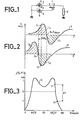
- Figure 1 shows a Yig ball oscillator, as described in patent No. 78.06431, filed March 7, 1978 in the name of the Applicant. This figure does not show the supply circuits of the field effect transistor 1, in order to simplify the electrical diagram. It will be the same, in the following text, for the other electrical diagrams of oscillators.
- the field effect transistor 1 of this oscillator has an output on its drain D which is charged by a standardized load 2, which is for example resistive at 50 ohms.
- the tuning dipole consists of a yttrium garnet ball 3 coupled by a half loop of wire 4 to the source of the field effect transistor.
- the reaction dipole is constituted by a yttrium garnet ball 5 coupled by a half loop of wire 6 to the gate of the same field effect transistor 1.
- the two Yig balls 3 and 5 are subjected to the same magnetic field H .
- FIG. 2 represents, as a function of the frequency given on the abscissa, the selfic reactance L or capacitive C of two Yig balls, the variations of which are represented by curves 7 and 8.
- L1 the selfic reactance L or capacitive C of two Yig balls
- C1 the reactance curve 7
- C2 the reactance curve 7
- a ball for example the one corresponding to curve 7, must have a reactive reactance LI, while the other ball, the one corresponding to curve 8 has a capacitive reactance C2. So that the two Yig balls are shifted in resonance frequency.
- the oscillation frequency of the oscillator thus formed is located in the frequency range between points 9 and 10, since it is between the abscissas of these points that one resonator is selfic while the other is capacitive.
- a first Yig ball has a resonant frequency fixed by its position in the magnetic field corresponding for example to point 11 on curve 7, the second Yig ball must have a resonant frequency corresponding to point 12 on curve 8, point 12 having the same frequency abscissa as point 11.
- FIG. 3 represents the curve of influence of the anisotropy of a Yig resonator on the resonance frequency.
- Yig is an anisotropic material, and its resonant frequency is a function of the orientation of its crystal lattice with respect to the magnetic field H.
- Figure 3 is shown the curve of response of a resonator to Yig, the orientation of its crystal lattice in degrees, relative to the direction of the magnetic field H, being given on the abscissa and a function of the oscillation frequency being given on the ordinate.
- the response curve 13 is a symmetrical curve, which is easy to imagine since during a rotation of 180 ° the network has two symmetrical positions relative to the field.
- the frequency band of the oscillator is obtained, as explained in the subject of FIG. 2, by shifting the resonances of the two Yig balls with respect to each other.
- the other ball must have a resonance frequency set at the complementary point 12, which gives a frequency interval ⁇ F.
- This frequency interval A F between the two Yig balls is especially necessary towards the lower frequencies, of the order of 6 to 10 GHz.
- the linearity curve of the oscillator is a function of this resonant frequency interval A F between the two balls.
- Figure 4 shows the role of each resonator in an oscillator with two resonators. This figure gives on the abscissa the frequencies of the oscillator, in GHz, and on the ordinate the difference on the linearity, in MHz, i.e. the difference between the intensity of control of the magnetic field H and the response given by the oscillator, its output frequency.
- the two Yig balls being of the same nature, follow the same law of linearity because they are in the same electromagnet, but because they are shifted in resonance frequency the two lines are translated relative to each other by A F.
- the upper line corresponds to the law of linearity of the so-called source ball, c ' that is to say the Yig ball coupled to the source of the transistor, and that the lower line corresponds to the law of linearity of the so-called grid ball, that is to say the Yig ball coupled to the grid this same transistor.
- the assembly of FIG. 4 can moreover be symmetrized with respect to the dotted line corresponding to a deviation 0, that is to say for which the linearity is absolutely perfect.
- an oscillator comprising two Yig balls in the configuration of FIG. 1 is an oscillator which can have a relatively wide frequency band, up to two octaves, but which has only a mediocre linearity AF / F, of the order of 10 -2 in relative.
- This oscillator comprises a field effect transistor 1, the drain of which is charged by an impedance 2, which is for example normalized to 50 ohms. Its source is joined to a tuning dipole constituted by a Yig 17 ball coupled to the source by a half loop of wire 18. Its grid is joined to a reaction dipole constituted in part by the same Yig 17 ball coupled by a half loop of wire 19, in series with a choke 20, relatively large taking into account the frequencies considered.
- the frequency response as a function of the H field is linear.
- the oscillation frequency takes place slightly before the resonance frequency of the Yig, on the inductive part of the reactance curve, as represented in L1, L2 in FIG. 2.
- the resonance frequency increases, the point d the oscillation descends along this inductive curve to a minimum value which is determined by the value of the transistor choke 20. Consequently, the upper oscillation frequency is determined by this inductor, but if this inductor is decreased, the lower oscillation frequency is noted, hence a limitation of the operating frequency band of the oscillator.
- FIG. 6 represents a simplified electric diagram of the oscillator according to the invention which takes account of the experience acquired by the oscillator with two Yig balls, which has a broad frequency band but a mediocre linearity and of the oscillator to a single Yig ball which has a limited frequency band but good linearity.
- the oscillator according to the invention comprises two Yig balls 21 and 22, coupled to the source and to the gate of the field effect transistor 1, charged on its drain by an impedance 2.
- the ball 21 is doubly coupled, it that is to say, it is by a half loop of wire 23 coupled to the source, which makes it a tuning reactance, and it is by a half loop of wire 24 coupled to the grid, which enters the reaction circuit.
- the ball 22 is coupled by a half loop of wire 25 to the gate of the field effect transistor, but the latter wire 25 is the same as that which already couples the ball 21 by a half loop of wire 24.
- the ball 21 is doubly coupled by two wires 23 and 24 respectively to the source and to the gate of the field effect transistor.
- one of the two oscillator wiring wires is doubly coupled at 24 and 25 to the two Yig balls 21 and 22 respectively.
- FIG. 8 represents the impedance curves of the doubly coupled resonator, that is to say the Yig ball 21 of FIG. 7.
- the upper curve, 26, of FIG. 8 represents the reactance of the Yig ball 21 in accordance with what has been exposed in FIG. 2.
- This Yig ball has a positive and self reactance represented by the part LI of curve greater than 0 and a capacitive part CI, less than 0 which therefore corresponds to a negative resistance.
- the point 9 at which this curve 26 passes through a zero reactance corresponds to the resonance frequency of the Yig ball.
- the median curve, marked 27 is the resistance curve brought back to the drain D of the field effect transistor 1 by the Yig ball. This resistance curve has a negative part, then a positive part and finally a cusp with again a negative part noted R1, when the frequency increases.
- the ball 21 therefore plays the role of source ball, and it is this which controls the frequencies of the oscillator in the region of lower frequencies, while the ball 22 plays the role of ball of grid and it is it which controls the frequencies of the oscillator in the field of the higher frequencies.
- FIG. 9 represents the linearity deviation curve of the oscillator according to the invention. This FIG. 9 resembles that of FIG. 4, but the scales are not the same there since it is an objective of the invention.
- the line of linear law of the grid ball that is to say the ball 22, is taken as the line of reference for the linearity deviations of the oscillator.
- the grid ball 22 which controls the oscillator and imposes the frequency: the difference A e on the linearity is very small.
- the source ball that is to say the doubly coupled ball 21, which drives the oscillator.
- this ball generates a negative resistance lower in frequency, and therefore it widens the frequency band, and on the other hand, given that at lower frequencies, it is it alone which drives the oscillator and that it is doubly coupled, it brings to the oscillator a good linearity in the range of the lower frequencies, which is more extended than in an oscillator with one or two balls, according to the known art.
- the interval A F, between the resonant frequencies of the two balls 21 and 22, is large, and it makes it possible to extend the frequency band, but nevertheless the difference in linearity ⁇ E, in the lower frequencies, remains very small.
- the oscillator according to the known art of FIG. 1 had a frequency band going from 4 to 22 GHz and a linearity of 10 -2 , that is to say 50 MHz at 10 GHz
- the oscillator according to the invention, of FIG. 6 has a frequency band going from 4 to 22 GHz, and a linearity deviation of ⁇ 10 Mhz.
- the oscillator according to the invention is used in microwave materials.
Landscapes
- Inductance-Capacitance Distribution Constants And Capacitance-Resistance Oscillators (AREA)
- Control Of Motors That Do Not Use Commutators (AREA)
Applications Claiming Priority (2)
| Application Number | Priority Date | Filing Date | Title |
|---|---|---|---|
| FR8416374 | 1984-10-26 | ||
| FR8416374A FR2572602B1 (fr) | 1984-10-26 | 1984-10-26 | Oscillateur a tres hautes frequences, a resonateurs gyromagnetiques |
Publications (2)
| Publication Number | Publication Date |
|---|---|
| EP0181801A1 true EP0181801A1 (de) | 1986-05-21 |
| EP0181801B1 EP0181801B1 (de) | 1988-11-30 |
Family
ID=9309015
Family Applications (1)
| Application Number | Title | Priority Date | Filing Date |
|---|---|---|---|
| EP85402047A Expired EP0181801B1 (de) | 1984-10-26 | 1985-10-22 | Oszillator sehr hoher Frequenz mit gyromagnetischen Resonatoren |
Country Status (6)
| Country | Link |
|---|---|
| US (1) | US4630002A (de) |
| EP (1) | EP0181801B1 (de) |
| JP (1) | JPS61105909A (de) |
| CA (1) | CA1267197A (de) |
| DE (1) | DE3566597D1 (de) |
| FR (1) | FR2572602B1 (de) |
Families Citing this family (11)
| Publication number | Priority date | Publication date | Assignee | Title |
|---|---|---|---|---|
| AT391231B (de) * | 1988-02-17 | 1990-09-10 | Akg Akustische Kino Geraete | Uhf-rueckkopplungsoszillator |
| JPH0287705A (ja) * | 1988-09-24 | 1990-03-28 | Mitsubishi Electric Corp | 同調形発振器 |
| US4988959A (en) * | 1989-10-31 | 1991-01-29 | Avantek, Inc. | YIG tuned oscillator using composite feedback |
| US5115209A (en) * | 1990-10-04 | 1992-05-19 | Wiltron Company | Multiple YIG oscillator |
| US5200713A (en) * | 1990-10-04 | 1993-04-06 | Wiltron Company | Multiple magnetically tuned oscillator |
| WO1992006534A1 (en) * | 1990-10-04 | 1992-04-16 | Wiltron Company | Multiple yig oscillator |
| US5801591A (en) * | 1997-05-13 | 1998-09-01 | Verticom, Inc. | Microwave linear oscillator/amplifier utilizing a multicoupled ferrite resonator |
| US6239664B1 (en) * | 1999-03-05 | 2001-05-29 | Rf Monolithics, Inc. | Low phase noise, wide tuning range oscillator utilizing a one port saw resonator and method of operation |
| GB0226394D0 (en) * | 2002-11-13 | 2007-03-28 | Bae Systems Plc | Radio frequency and microwave signals |
| JP4547502B2 (ja) * | 2004-09-15 | 2010-09-22 | コミサリア、ア、レネルジ、アトミク、エ、オ、エネルジ、アルテルナティブ | 強磁性薄膜同調マイクロ波発振器 |
| US9819308B1 (en) * | 2017-01-30 | 2017-11-14 | Micro Lambda Wireless, Inc. | System and method for reducing phase noise in high frequency YIG oscillators |
Citations (2)
| Publication number | Priority date | Publication date | Assignee | Title |
|---|---|---|---|---|
| US3879677A (en) * | 1973-07-20 | 1975-04-22 | Varian Associates | Tuned oscillator circuit having a tuned filter output |
| GB2016232A (en) * | 1978-03-07 | 1979-09-19 | Thomson Csf | Oscillator tunable within a very wide frequency band |
Family Cites Families (1)
| Publication number | Priority date | Publication date | Assignee | Title |
|---|---|---|---|---|
| US3339152A (en) * | 1965-10-24 | 1967-08-29 | Gold Line Company | Magnetically tuned ferrite cavity transistor oscillator |
-
1984
- 1984-10-26 FR FR8416374A patent/FR2572602B1/fr not_active Expired
-
1985
- 1985-10-04 US US06/784,603 patent/US4630002A/en not_active Expired - Fee Related
- 1985-10-22 EP EP85402047A patent/EP0181801B1/de not_active Expired
- 1985-10-22 DE DE8585402047T patent/DE3566597D1/de not_active Expired
- 1985-10-23 JP JP60237161A patent/JPS61105909A/ja active Granted
- 1985-10-23 CA CA000493655A patent/CA1267197A/en not_active Expired
Patent Citations (2)
| Publication number | Priority date | Publication date | Assignee | Title |
|---|---|---|---|---|
| US3879677A (en) * | 1973-07-20 | 1975-04-22 | Varian Associates | Tuned oscillator circuit having a tuned filter output |
| GB2016232A (en) * | 1978-03-07 | 1979-09-19 | Thomson Csf | Oscillator tunable within a very wide frequency band |
Non-Patent Citations (2)
| Title |
|---|
| 1981 IEEE MTT-S INTERNATIONAL MICROWAVE SYMPOSIUM DIGEST, 1981, pages 141,142, IEEE, New York, US; J. OBREGON et al.: "Decade bandwidth FET functions" * |
| IEEE INTERNATIONAL SOLID-STATE CIRCUITS CONFERENCE, vol. 22, 15 février 1979, pages 162,163, IEEE, New York, US; Y. LE TRON et al.: "Multioctave FET oscillators double tuned by a single YIG" * |
Also Published As
| Publication number | Publication date |
|---|---|
| EP0181801B1 (de) | 1988-11-30 |
| JPS61105909A (ja) | 1986-05-24 |
| FR2572602B1 (fr) | 1986-12-12 |
| CA1267197A (en) | 1990-03-27 |
| DE3566597D1 (en) | 1989-01-05 |
| JPH0584962B2 (de) | 1993-12-03 |
| US4630002A (en) | 1986-12-16 |
| FR2572602A1 (fr) | 1986-05-02 |
Similar Documents
| Publication | Publication Date | Title |
|---|---|---|
| EP0181801B1 (de) | Oszillator sehr hoher Frequenz mit gyromagnetischen Resonatoren | |
| EP0367657B1 (de) | Mikrowellen-Phasenschieber mit O- oder Pi-Phasenverschiebung | |
| EP0190613A1 (de) | Mikrowellendiskriminator und dessen Verwendung | |
| FR2607643A1 (fr) | Commutateur a semiconducteurs a micro-ondes | |
| EP0321329A1 (de) | Mittels Varaktoren abgestimmter Oszillator-Frequenzverdoppler | |
| EP0242292A1 (de) | Spannungsgesteuerter Oszillator-Frequenverdoppler | |
| FR2644647A1 (fr) | Oscillateur hyperfrequence commande en tension | |
| EP0859458B1 (de) | Schaltung zur Frequenzmodulation eines Quarzoszillators | |
| FR2971629A1 (fr) | Filtre radiofrequences reglable en technologie coplanaire et procede de reglage du filtre | |
| EP0596562B1 (de) | Vorrichtung mit einer Schaltung zum Verarbeiten eines Wechselsignals | |
| WO1993000718A1 (fr) | Dispositif de filtrage coupe-bande hyperfrequence accordable | |
| FR2625052A1 (fr) | Circuit hyperfrequences comprenant au moins un transistor a effet de champ charge | |
| EP0347985B1 (de) | Allpasstyp-Schaltung für ultrahohe Frequenzen | |
| EP0143041A2 (de) | Einrichtung zur Kompensation der Beschleunigungsempfindichkeit eines Oszillators | |
| EP0160587B1 (de) | Frequenzregelung eines Filters mit gyromagnetischen Resonatoren | |
| EP0113264B1 (de) | Hochfrequenz-Oszillator mit kompensiertem Isochronismusmangel | |
| CA1112727A (fr) | Filtre electrique de frequence a cristaux piezoelectriques | |
| EP0312145B1 (de) | Aktive, einen RC-Filter bildende Schaltung für Bandsperre oder Allpass-Anwendung | |
| EP0128612A1 (de) | Schaltung mit einer temperatur-variablen Kapazität und frequenzstabilisierter Hyperfrequenzoszillator mit einer solchen Schaltung | |
| EP0337825B1 (de) | Mikrowellensperrfilter in Mikrostreifenausführung | |
| EP0398442B1 (de) | Halbleiteranordnung mit einem aktiven Filter im hohen und ultrahohen Frequenzgebiet | |
| BE472935A (de) | ||
| EP0309332B1 (de) | Quarzoszillatorschaltung, deren Frequenz durch thermische Wirkung gesteuert wird | |
| FR2785745A1 (fr) | Circuit haute frequence a dephasage variable | |
| FR2605461A1 (fr) | Resonateur ferromagnetique pour circuits en hyperfrequences |
Legal Events
| Date | Code | Title | Description |
|---|---|---|---|
| PUAI | Public reference made under article 153(3) epc to a published international application that has entered the european phase |
Free format text: ORIGINAL CODE: 0009012 |
|
| AK | Designated contracting states |
Kind code of ref document: A1 Designated state(s): DE GB IT NL SE |
|
| 17P | Request for examination filed |
Effective date: 19860606 |
|
| 17Q | First examination report despatched |
Effective date: 19880315 |
|
| GRAA | (expected) grant |
Free format text: ORIGINAL CODE: 0009210 |
|
| AK | Designated contracting states |
Kind code of ref document: B1 Designated state(s): DE GB IT NL SE |
|
| PG25 | Lapsed in a contracting state [announced via postgrant information from national office to epo] |
Ref country code: NL Effective date: 19881130 |
|
| ITF | It: translation for a ep patent filed | ||
| REF | Corresponds to: |
Ref document number: 3566597 Country of ref document: DE Date of ref document: 19890105 |
|
| GBT | Gb: translation of ep patent filed (gb section 77(6)(a)/1977) | ||
| NLV1 | Nl: lapsed or annulled due to failure to fulfill the requirements of art. 29p and 29m of the patents act | ||
| RAP4 | Party data changed (patent owner data changed or rights of a patent transferred) |
Owner name: THOMSON-CSF |
|
| PLBE | No opposition filed within time limit |
Free format text: ORIGINAL CODE: 0009261 |
|
| STAA | Information on the status of an ep patent application or granted ep patent |
Free format text: STATUS: NO OPPOSITION FILED WITHIN TIME LIMIT |
|
| 26N | No opposition filed | ||
| PG25 | Lapsed in a contracting state [announced via postgrant information from national office to epo] |
Ref country code: DE Effective date: 19900703 |
|
| ITTA | It: last paid annual fee | ||
| EAL | Se: european patent in force in sweden |
Ref document number: 85402047.6 |
|
| PGFP | Annual fee paid to national office [announced via postgrant information from national office to epo] |
Ref country code: SE Payment date: 19970917 Year of fee payment: 13 |
|
| PGFP | Annual fee paid to national office [announced via postgrant information from national office to epo] |
Ref country code: GB Payment date: 19970918 Year of fee payment: 13 |
|
| PG25 | Lapsed in a contracting state [announced via postgrant information from national office to epo] |
Ref country code: GB Free format text: LAPSE BECAUSE OF NON-PAYMENT OF DUE FEES Effective date: 19981022 |
|
| PG25 | Lapsed in a contracting state [announced via postgrant information from national office to epo] |
Ref country code: SE Free format text: LAPSE BECAUSE OF NON-PAYMENT OF DUE FEES Effective date: 19981023 |
|
| GBPC | Gb: european patent ceased through non-payment of renewal fee |
Effective date: 19981022 |
|
| EUG | Se: european patent has lapsed |
Ref document number: 85402047.6 |