EP0181819B1 - Dispositif d'évacuation d'alimentation d'une cellule de mémoire - Google Patents
Dispositif d'évacuation d'alimentation d'une cellule de mémoire Download PDFInfo
- Publication number
- EP0181819B1 EP0181819B1 EP85402151A EP85402151A EP0181819B1 EP 0181819 B1 EP0181819 B1 EP 0181819B1 EP 85402151 A EP85402151 A EP 85402151A EP 85402151 A EP85402151 A EP 85402151A EP 0181819 B1 EP0181819 B1 EP 0181819B1
- Authority
- EP
- European Patent Office
- Prior art keywords
- supply bus
- bias supply
- common bias
- memory
- memory cell
- Prior art date
- Legal status (The legal status is an assumption and is not a legal conclusion. Google has not performed a legal analysis and makes no representation as to the accuracy of the status listed.)
- Expired - Lifetime
Links
- 230000015654 memory Effects 0.000 title claims description 82
- 238000000034 method Methods 0.000 title claims description 10
- 230000002000 scavenging effect Effects 0.000 title description 2
- 230000003068 static effect Effects 0.000 claims description 18
- 230000002093 peripheral effect Effects 0.000 description 12
- 238000010586 diagram Methods 0.000 description 6
- 230000006870 function Effects 0.000 description 2
- 238000002955 isolation Methods 0.000 description 2
- 238000011084 recovery Methods 0.000 description 2
- 239000004065 semiconductor Substances 0.000 description 2
- 230000000694 effects Effects 0.000 description 1
- 238000004519 manufacturing process Methods 0.000 description 1
- 229910044991 metal oxide Inorganic materials 0.000 description 1
- 150000004706 metal oxides Chemical class 0.000 description 1
- 238000012986 modification Methods 0.000 description 1
- 230000004048 modification Effects 0.000 description 1
- 230000003071 parasitic effect Effects 0.000 description 1
- 229910021420 polycrystalline silicon Inorganic materials 0.000 description 1
- 229920005591 polysilicon Polymers 0.000 description 1
- 239000000758 substrate Substances 0.000 description 1
- 230000007704 transition Effects 0.000 description 1
Images


Classifications
-
- G—PHYSICS
- G11—INFORMATION STORAGE
- G11C—STATIC STORES
- G11C5/00—Details of stores covered by group G11C11/00
- G11C5/14—Power supply arrangements, e.g. power down, chip selection or deselection, layout of wirings or power grids, or multiple supply levels
-
- G—PHYSICS
- G11—INFORMATION STORAGE
- G11C—STATIC STORES
- G11C11/00—Digital stores characterised by the use of particular electric or magnetic storage elements; Storage elements therefor
- G11C11/21—Digital stores characterised by the use of particular electric or magnetic storage elements; Storage elements therefor using electric elements
- G11C11/34—Digital stores characterised by the use of particular electric or magnetic storage elements; Storage elements therefor using electric elements using semiconductor devices
- G11C11/40—Digital stores characterised by the use of particular electric or magnetic storage elements; Storage elements therefor using electric elements using semiconductor devices using transistors
- G11C11/41—Digital stores characterised by the use of particular electric or magnetic storage elements; Storage elements therefor using electric elements using semiconductor devices using transistors forming static cells with positive feedback, i.e. cells not needing refreshing or charge regeneration, e.g. bistable multivibrator or Schmitt trigger
- G11C11/413—Auxiliary circuits, e.g. for addressing, decoding, driving, writing, sensing, timing or power reduction
- G11C11/414—Auxiliary circuits, e.g. for addressing, decoding, driving, writing, sensing, timing or power reduction for memory cells of the bipolar type
-
- G—PHYSICS
- G11—INFORMATION STORAGE
- G11C—STATIC STORES
- G11C8/00—Arrangements for selecting an address in a digital store
- G11C8/08—Word line control circuits, e.g. drivers, boosters, pull-up circuits, pull-down circuits, precharging circuits, for word lines
Definitions
- This invention relates generally to digital computer memory cells and particularly to apparatus and methods for supplying standby current to a static bipolar random access memory. Still more particularly, this invention relates to apparatus and methods for supplying standby current to a bipolar static random access memory cell to maintain a stored logic state.
- a static semiconductor memory cell has the ability to store data indefinitely as long as sufficient power, known as the "standby power" is applied to the cell.
- a dynamic memory requires that the stored data be periodically rewritten to prevent the data from becoming lost.
- Static memory cells are essentially flip flops that can maintain a given state indefinitely whereas dynamic memory cells use capacitances that must be periodically recharged.
- the memory cell standby current flows from the most positive power supply to the most negative power supply and has no useful function other than providing the power required to maintain a stored logic state.
- An improved static RAM uses the standby current from a first group of memory cells to supply to the power for a second group of memory cells.
- the memory speed of a static RAM is a function of the standby power applied such that greater standby power results in a faster memory.
- Sophisticated digital computers require very fast memories. Accordingly, there is a need in the art for a bipolar static ECL RAM cell which better utilizes the available power to provide a memory speed superior to that of prior devices. Further, there is a need for greater efficiency in the use of standby power in integrated systems.
- the present invention relates to a system and method for more efficiently utilizing the standby power that is available in an integrated circuit in a system comprised of individual circuits.
- the result can be either increased circuit speed because more standby power is available for application to circuits in the system that were previously power starved, or power savings in that less power is needed for operating the circuit because of more efficient utilization of a given amount of power made available to the circuit.
- the invention may be used with any system having individual subsystems that operate over different ranges of voltage and that require standby power. The invention is set forth in claims 1 and 14.
- the current required to maintain the memory cell in a preset state flows from the V CC source through a first biasing resistor and through a row of parallel memory cells. After leaving the memory cells, the current passes through an isolation device, which may be a second resistor or a transistor, to a common bias supply bus. From the common bias supply bus the current is directed to peripheral circuits, such as decoders.
- a shunt voltage regulator limits the dependence of the common bias supply bus voltage on the currents sourced by the memory cells and sunk by the peripheral circuits connected to the common bias supply bus.
- the first resistors in series with the parallel group of memory cells and the isolation device provide means for changing the bias on a particular row of memory cells when it is addressed without disturbing the bias on other memory cell rows.
- the reference voltages of each of the peripheral circuits can be made independent of the common bias supply bus voltage and independent of the other peripheral circuits by the use of a local voltage regulator on each peripheral.
- the invention in a second preferred embodiment of the invention used with ECL static RAM cells that are addressed by placing the word line in a logic high state, includes a transistor connected to the common bias supply bus for supplying standby current to each of a plurality of parallel rows of memory cells. Peripheral circuits connected to the common bias supply bus supply current thereto through appropriate resistors. The decoder currents are used to supply the standby current to the memory cells when they are in the deaddressed state. When a row of memory cells is addressed, the row receives current from the U cc supply.
- a typical diode coupled memory circuit 24 includes a pair of transistors Q1 and Q2.
- the collectors of the transistors Q1 and Q2 are connected through load resistors R1 and R2, respectively, to a power supply (not shown) having a voltage output V cc that is applied to a resistor R3.
- the junctions of the resistors R1 and R2 with the collectors of the transistors Q1 and Q2 are sometimes hereinafter referred to as nodes A and B, respectively.
- the collector of the transistor Q1 is connected to node A, which is connected to the base of the transistor Q2, and the collector of the transistor Q2 is connected to the node B which is connected to the base of the transistor Q1.
- the emitters of the transistors Q1 and Q2 are coupled together and are connected to a word address line 26 at a junction hereinafter referred to as node C.
- the diode coupled memory circuit 24 usually has a Schottky diode 28 connected to node A and a Schottky diode 30 connected to node B.
- the Schottky diodes 28 and 30 allow a considerable increase in cell current during cell selection to enhance read and write performance as is well known by those skilled in the art.
- the memory circuit 24 is addressed by dropping the word line 26 to a logic low state and deaddressed by raising it to a logic high state.
- One of the transistors Q1 or Q2 will be on while the memory circuit 24 is in the standby mode, and addressing the cell 24 by applying a logic low to the word line 26 causes a current to flow from V cc through the conducting transistor Q1 or Q2 to the word line 26.
- the voltages at nodes A and B are indicative of a logic state that has been previously stored in the memory circuit 24. If Q2 is on, then the voltage at node A, V A , is greater than the voltage at node B, V B .
- node C goes high, which allows both the transistors Q1 and Q2 to be off. Even after Q2 turns off there is still a voltage difference U AB between the nodes A and B.
- the resistors R1 and R2 provide paths for the bias voltage V cc to charge the parasitic capacitances 32 and 34 between nodes A and B and node C, respectively, after the transistors Q1 and Q2 turn off.
- the voltages V A and V B rise together, maintaining the differential V AB that existed before the call 24 was addressed.
- the voltages V A and U B rise until the transistor Q1 or Q2 that was on before the cell 24 was addressed turns on again so that after the memory cell 24 is deaddressed, it returns to its former logic state.
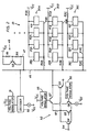
- Figure 2 illustrates a static RAM 35 that includes a plurality of diode coupled memory circuits that are substantially identical to the memory circuit 24.
- the memory circuits are arranged in a plurality of rows 36A, 36B, 36C, etc., with the row 36A containing, for example, four memory circuits, 38A, 39A, 40A and 41A.
- the rows 36B and 36C contain four memory circuits 38B, 39B, 40B, 41B, and 38C, 39C, 40C and 41C, respectively.
- Each row 36 may correspond to a word in the static RAM 35.
- Each of the ECL circuits in the rams 36A, 36B, 36C, etc. is connected to a word line 44A, 44B, 44C, etc.
- the ECL circuits in each row 36A, 36B, 36C, etc. are connected in parallel and receive current from a power source V cc through resistors R3A, R3B, R3C, etc.
- the current output of each row 36A, 36B, 36C, etc. passes through a resistor R4A, R4B, R4C, etc., respectively to a common bias supply bus 46.
- the resistors R3A, R3B, etc. and the resistors R4A, R4B, etc. may be conveniently formed of polysilicon using well-known integrated circuit fabrication techniques; or they may be transistors properly biased to have the desired resistances.
- the power supply V cc is connected to a voltage regulator 48, which may include a resistor R5 connected to V cc and between the base and collector of a transitor Q3.
- a resistor R6 is connected between the emitter and base of the transistor Q3.
- the output 47 of the voltage regulator 48 is taken between the emitter of Q3 and the resistor R6.
- the output 47 is maintained by the voltage regulator 48 at a constant voltage and is connected to the common bias supply bus bus 46.
- the voltage regulator 48 maintains an essentially constant voltage an the common bias supply bus 46 even if the amount current supplied thereto from the rows 36A, 36B, etc. varies as they are addressed and deaddressesd.
- the common bias supply bus 46 is connected to one or more peripheral circuits.
- the peripheral circuits may, in general, include any circuit that requires a power supply more negative than V cc ; but for simplicity of illustration and explanation, Figure 2 illustrates a pair of decoders 50 and 52 connected to the common bias supply bus 46.
- the decoders 50 and 52 are essentially identical in structure; therefore only the decoder 52 is discussed in detail.
- the decoder 52 includes an input port 54 connected to the base of a transistor Q4.
- the collector and emitter of the transistor Q4 are connected to the collector and emitter of a transistor Q5.
- a resistor R7 is connected to the collectors of the transistors Q4 and Q5 and to the emitter of a transistor Q7.
- the emitter of the transistor Q7 and the resistor R7 are connected to the collector of a transistor Q8.
- the power supply V cc provides an input to a voltage regulator 55, which has an output connected to the base of the transistor Q7.
- a current sunk to a power supply V ee is connected to the emitters of the transistors Q4, Q5 and Q8.
- a voltage regulator 56 is connected to the base of the transistor Q8.
- the base of a transistor Q9 is connected to the collectors of the transistors Q4 and Q5, and the collectors of the transistors Q9 and Q7 are connected to the common bias supply bus 46.
- the output of the decoder 52 is taken from the emitter of the transistor Q9.
- the memory cells each draw a standby current of, for example, 1 ⁇ A in the deaddressed state.
- the total standby current is therefore 64 milliamperes, which, as shown in Figure 2, is input to the common bias supply bus 46 for supplying power to the decoders 50 and 52 before the current is sunk to the power supply V ee , rather than being sunk directly to V ee as in the prior art.
- the resistors R4A, R4B, R4C, etc. must have resistances sufficiently large that changes on the word lines 44A, 44B, 44C, etc., respectively, do not have a significant effect on the voltage of the common bias supply bus 46.
- the common bias supply bus 46 acts as a low impedance current source. Voltage changes on the common bias supply bus 46 are acceptable if the decoders 50 and 52 and other peripherals (not shown) connected to the common bias supply bus include voltage regulators, such as voltage regulator 55, to ensure the application of constant voltage to the decoders. Voltage regulators are essential if the various peripherals require different voltages.
- each memory cell row has essentially the same structure, only the row 36C is hereinafter discussed in detail.
- the resistors R3C and R4C are used to select the bias on the row 36C.
- the value of R4C is not critical to power scavenging, but since R4C is a means for isolating the row 36C from the common bias supply bus 46 when the row is addressed, the ohmic value of R4C may be critical in the logic design of the static RAM 35.
- the time constant of R4C and the capacitance of the node 44C or the internal cell nodes to the substrate set the recovery time of the transition from the addressed state to the deaddressed state.
- the word line 44C should be brought up rapidly so that a new word line may be addressed without causing an ambiguity in the data output of the static RAM 35.
- the resistor R4C must be large enough to limit voltage swings on the common bias supply bus 46 and small enough to provide the desired recovery time.
- Figure 3 illustrates an alternative means for isolating the word line 44C from the common bias supply bus 46.
- a transistor Q10 which may be formed of a suitable metal oxide semiconductor (MOS) or a bipolar device, is connected between the work line 44c and the common bias supply bus 46 so as to be able to allow current flow between the common bias supply bus 46 and the word line 44c or shut the word line off, depending on the state of a control signal V CTL .
- the transistor Q10 is biased on by the V CTL signal when the row 36C is deaddressed so that the standby current from the row 36C may flow through the word line 44C to the common bias supply bus 46.
- the transistor Q10 When the row 36C is addressed, the transistor Q10 is turned off to isolate the word line 44C from the common bias supply bus 46, and a second MOS transistor Q11 is switched on to pull down the word line 44C.
- the transistor Q11 When the row 36C is deaddressed, the transistor Q11 is turned off; and the transistor Q10 is turned on by the U CTL signal.
- the signal U CTL may be derived by known decoder circuitry coupled to the address inputs to turn the transistor Q10 off when the row to which the word line 44c is connected, is addressed.
- FIG. 4 illustrates a diagram of an ECL circuit 60 that is addressed by taking the word line high and deaddressed by taking the word line low as is well known by those skilled in the art.
- the ECL circuit 60 includes a first multiemitter transistor Q12, Q14 and a second multiemitter transistor Q13, Q15.
- a pair of bit lines 62 and 64 are connected to the emitters Q12 and Q13, respectively, while both emitters Q14 and Q15 are coupled to a word line 66.
- the bit lines 62 and 64 are driven low when the ECL circuit 60 is addressed.
- an ECL static RAM 70 includes a plurality of rows 72A, 72B, etc., of ECL circuits that are substantially identical to the ECL circuit 60.
- the ECL circuits 60 are connected in parallel in each row 72A, 72B, etc. which may include any desired number of such circuits; and each row has a word line, such as the word line 80 for row 72A, the word line 78 for the row 72B, etc.
- a voltage regulator 75 which is substantially identical to the voltage regulator 48, is connected to the bases of a pair of transistors Q19 and Q20.
- the emitters of the transistors Q19 and Q20 are coupled to the word lines 80 and 78, respectively; and the collectors of the transistors Q19 and Q20 are coupled to the common bias supply bus bus 77.
- the transistors Q19 and Q20 supply current to the word lines 80 and 78, respectively, during the deaddressed state.
- the voltage regulator 75 regulates the voltage on the bases of the transistors Q19 and Q20 to maintain an essentially constant standby voltage supply to the word lines 80 and 78 in the deaddressed state.
- One or more peripheral circuits such as a decoder 76 are also connected to the common bias supply bus 77.
- the decoder 76 includes a resistor R8 connected between the power supply V cc and the base of a transistor Q16.
- the collector of the transistor Q16 is connected to the power supply V cc .
- the emitter of the transistor Q16 is connected to the word line 78 of the row 72B to supply current to the word line 78 when the row 72B is addressed.
- the base of the transistor Q16 and the resistor R8 are connected to the collectors of a pair of transistors Q17 and Q18.
- the emitters of the transistors Q17 and Q18 are connected together to a resistor R9, which is connected to the common bias supply bus bus 77.
- the bases of the transistors Q17 and Q18 serve as the inputs for the decoder 76.
- a shunt voltage regulator 73 coupled to the common bias supply bus 77 maintains the voltage on the common bias supply bus 77 essentially constant regardless of fluctuations in standby current in the word lines 78 and 80.
- any desired number of memory cell rows and decoders may be connected to the common bias supply bus bus 77.
- the two rows 72A and 72B and the decoder 76 are shown in Figure 5 only for purposes of illustrating and explaining the structure and method of operation of the invention.
- Each cell in an ECL static RAM of the type shown in Figure 5 typically requires a standby current of about 2 ⁇ A for a 16K RAM.
- a 1K RAM requires about 30 ⁇ A per cell in the standby mode.
- the decoder 76 When the decoder 76 receives signals at the bases of the transistors Q17 and Q18 indicating that the row 72B is not being addressed, current from Q17 and Q18 passes through the resistor R9 to the common bias supply bus bus 77, which then applies this current to the word lines 80 and 78 through the transistors Q19 and Q20.
- the voltage regulator 75 must provide adequate bias to the bases of the transistors Q19 and Q20 so that the transistors Q19 and Q20 are able to supply sufficient standby current to the word lines 80 and 78, respectively.
- the transistor Q16 turns on and current flows out of the emitter of the transistor Q16 to the word line 78 to address the row 72B.
- the transistor Q20 turns off to isolate the row 72B from the common bias supply bus 77.
Landscapes
- Engineering & Computer Science (AREA)
- Microelectronics & Electronic Packaging (AREA)
- Computer Hardware Design (AREA)
- Power Engineering (AREA)
- Static Random-Access Memory (AREA)
Claims (17)
- Système à mémoire comprenant plusieurs cellules de mémoire (36A/B/C, 72A/B),
une unique alimentation en énergie présentant une première (VCC) et une seconde (VEE) sorties de niveau de tension, lesdites cellules de mémoire étant connectées à l'une desdites sorties de niveau de tension et étant alimentées dans leur état non adressé, par un courant de repos à partir de ladite première sortie de niveau de tension,
un bus d'alimentation de polarisation commun (46, 77), commun à ladite pluralité de cellules de mémoire et recevant lesdits courants de repos qui ont traversé lesdites cellules de mémoire, ledit bus d'alimentation de polarisation commun présentant un niveau de tension intermédiaire situé entre ledit premier et ledit second niveaux,
au moins un circuit (50, 52, 76) connecté entre ledit bus d'alimentation de polarisation commun et ladite autre sortie parmi lesdites sorties de niveau de tension pour recevoir au moins une certaine quantité dudit courant de repos,
des moyens pour adresser des cellules choisies parmi lesdites cellules de mémoire, et
des moyens (R4A, R4B, R4C, Q10, Q19, Q20) pour pratiquement isoler les cellules de mémoire adressées dudit but d'alimentation de polarisation commun,
caractérisé en ce que ledit second circuit comprend un décodeur (50, 52, 76) affecté auxdites cellules de mémoire. - Le système suivant la revendication 1, caractérisé en se qu'il comprend également des moyens de régulation de tension (48, 73) raccordés audit bus d'alimentation de polarisation commun (46, 77) pour maintenir la tension qui lui est appliquée à une valeur relativement constante en dépit des fluctuations du courant de fonctionnement qui en est prélevé.
- Le système suivant la revendication 1, caractérisé en ce qu'une pluralité desdites cellules de mémoire est agencée selon une rangée;
en ce que les rangées de cellules de mémoire sont adressées sélectivement et en ce que chaque rangée de cellules de mémoire adressée est à peu près isolée dudit bus d'alimentation de polarisation commun (46, 77) de telle manière que les fluctuations du courant de repos provenant desdites rangées et provoquées par des transitions entre les états adressés et non adressés, n'affectent pas de façon appréciable le niveau de tension dudit bus d'alimentation de polarisation commun. - Le système suivant la revendication 1 ou 3, caractérisé en ce que lesdits moyens d'isolation comprennent une résistance (R4C) connectée entre lesdites cellules de mémoire et ledit bus d'alimentation de polarisation commun (46).
- Le système suivant la revendication 4, caractérisé en ce que ladite résistance (R4C) est choisie pour avoir une valeur qui soit suffisamment élevée pour éviter pratiquement toute dérivation du courant à partir du bus d'alimentation de polarisation commun lorsque la cellule de mémoire (36C) connectée à ladite résistance est adressée, et une valeur qui soit suffisamment faible pour pratiquement ne pas empêcher la circulation du courant de repos entre ladite cellule de mémoire (36C) et ledit bus d'alimentation de polarisation commun (46) lorsque ladite cellule de mémoire n'est plus adressée.
- Le système suivant la revendication 4 ou 5. caractérisé en ce qu'il comprend également des moyens (R3C) pour polariser ladite cellule de mémoire afin d'établir un courant prédéterminé de repos.
- Le système suivant la revendication 6, caractérisé en ce que lesdits moyens de polarisation (R3C) comprennent une résistance de polarisation connectée entre ladite cellule de mémoire (36C) et ladite alimentation (VCC).
- Le système suivant la revendication 1 ou 3, caractérisé en ce que lesdits moyens d'isolation comprennent un dispositif de commutation (Q10, Q20) connecté entre ladite cellule de mémoire et ledit bus d'alimentation de polarisation commun (46, 77), ledit dispositif de commutation (Q10, Q20) étant dans l'état conducteur lorsque le courant de repos traverse ladite cellule de mémoire, ledit dispositif de commutation (Q10, Q20) étant dans l'état non conducteur lorsque ladite cellule de mémoire est adressée afin de limiter la circulation de courant électrique entre ladite cellule de mémoire et le bus d'alimentation de polarisation commun (46, 77).
- Le système suivant la revendication 8, caractérisé en ce que ledit dispositif de commutation comprend un transistor de commutation (Q10, Q20).
- Le système suivant la revendication 9, caractérisé en ce que ledit transistor de commutation (Q10) comprend un trajet de commutation et un noeud de commutation pour recevoir un signal qui commande la circulation du courant à travers ledit trajet de commutation, ledit transistor ayant son trajet de commutation raccordé entre sa cellule de mémoire associée (36C) et ledit bus d'alimentation de polarisation commun (46) et son noeud de commutation raccordé à un signal (VCTL) provenant desdits moyens assurant l'adressage sélectif de telle sorte que ledit trajet de commutation soit conducteur lorsque ladite cellule de mémoire (36C) n'est pas adressée et non conducteur, lorsque ladite cellule de mémoire est adressée.
- Le système suivant la revendication 2, caractérisé en ce que lesdits moyens de régulation de tension (48, 73) raccordés audit bus d'alimentation de polarisation commun (46, 77) limitent les fluctuations de tension sur ce bus lorsque la cellule de mémoire (36C, 72B) passe de l'état adressé à l'état non adressé.
- Le système suivant l'une quelconque des revendications précédentes, caractérisé en ce que chacune des cellules de mémoire comprend une cellule de mémoire (60) à couplage par émetteurs.
- Le système suivant l'une quelconque des revendications 1 à 11, caractérisé en ce que chacune desdites cellules de mémoire comprend une cellule de mémoire (24) à couplage par diodes.
- Un procédé pour appliquer du courant de repos à partir d'une source d'énergie à une mémoire statique à accès aléatoire tel que défini dans la revendication 1, caractérisé en ce qui consiste à :
passer le courant de repos à travers un circuit de mémoire non adressé et à travers un bus d'alimentation de polarisation commun, et
passer au moins une partie dudit courant de repos à travers un circuit comprenant un décodeur de mémoire et couplé audit bus d'alimentation de polarisation commun. - Le procédé selon la revendication 14, caractérisé en ce qu'il consiste également à :
adresser le circuit de mémoire; et
isoler le circuit de mémoire dudit bus d'alimentation de polarisation commun lorsque le circuit de mémoire est adressé. - Le procédé selon la revendication 15, caractérisé en ce que l'étape d'isolation consiste à fournir une résistance entre le circuit de mémoire et le bus commun d'alimentation de polarisation.
- Le procédé selon la revendication 15, caractérisé en ce que ladite étape d'isolation consiste à :
fournir un dispositif de commutation entre le circuit de mémoire et ledit bus d'alimentation de polarisation commun; et
changer l'état du dispositif de commutation d'un état conducteur à un état non conducteur lorsque le circuit de mémoire est adressé.
Applications Claiming Priority (2)
| Application Number | Priority Date | Filing Date | Title |
|---|---|---|---|
| US06/669,929 US4627034A (en) | 1984-11-09 | 1984-11-09 | Memory cell power scavenging apparatus and method |
| US669929 | 1996-06-25 |
Publications (3)
| Publication Number | Publication Date |
|---|---|
| EP0181819A2 EP0181819A2 (fr) | 1986-05-21 |
| EP0181819A3 EP0181819A3 (en) | 1988-06-08 |
| EP0181819B1 true EP0181819B1 (fr) | 1993-04-21 |
Family
ID=24688311
Family Applications (1)
| Application Number | Title | Priority Date | Filing Date |
|---|---|---|---|
| EP85402151A Expired - Lifetime EP0181819B1 (fr) | 1984-11-09 | 1985-11-07 | Dispositif d'évacuation d'alimentation d'une cellule de mémoire |
Country Status (5)
| Country | Link |
|---|---|
| US (1) | US4627034A (fr) |
| EP (1) | EP0181819B1 (fr) |
| JP (1) | JPS61160895A (fr) |
| CA (1) | CA1238419A (fr) |
| DE (1) | DE3587283T2 (fr) |
Families Citing this family (7)
| Publication number | Priority date | Publication date | Assignee | Title |
|---|---|---|---|---|
| JPS6145491A (ja) * | 1984-08-10 | 1986-03-05 | Fujitsu Ltd | 半導体記憶装置 |
| US4792923A (en) * | 1985-08-30 | 1988-12-20 | Mitsubishi Denki Kabushiki Kaisha | Bipolar semiconductor memory device with double word lines structure |
| JPH0770216B2 (ja) * | 1985-11-22 | 1995-07-31 | 株式会社日立製作所 | 半導体集積回路 |
| IL83184A0 (en) * | 1986-07-15 | 1987-12-31 | Sundstrand Data Control | Method and apparatus for memory mapping topographical data |
| US5663919A (en) * | 1996-02-28 | 1997-09-02 | Micron Technology, Inc. | Memory device with regulated power supply control |
| US7298152B1 (en) | 2006-05-19 | 2007-11-20 | The Boeing Company | Damage detection system |
| US8594882B2 (en) * | 2008-01-16 | 2013-11-26 | The Boeing Company | Damage detection system |
Family Cites Families (6)
| Publication number | Priority date | Publication date | Assignee | Title |
|---|---|---|---|---|
| JPS576198B2 (fr) * | 1974-08-09 | 1982-02-03 | ||
| FR2443118A1 (fr) * | 1978-11-30 | 1980-06-27 | Ibm France | Dispositif pour l'alimentation des memoires monolithiques |
| JPS5831673B2 (ja) * | 1979-08-22 | 1983-07-07 | 富士通株式会社 | 半導体記憶装置 |
| JPS5677981A (en) * | 1979-11-28 | 1981-06-26 | Oki Electric Ind Co Ltd | Memory access circuit |
| US4422162A (en) * | 1980-10-01 | 1983-12-20 | Motorola, Inc. | Non-dissipative memory system |
| US4488263A (en) * | 1982-03-29 | 1984-12-11 | Fairchild Camera & Instrument Corp. | Bypass circuit for word line cell discharge current |
-
1984
- 1984-11-09 US US06/669,929 patent/US4627034A/en not_active Expired - Lifetime
-
1985
- 1985-11-07 EP EP85402151A patent/EP0181819B1/fr not_active Expired - Lifetime
- 1985-11-07 DE DE85402151T patent/DE3587283T2/de not_active Expired - Fee Related
- 1985-11-08 CA CA000494919A patent/CA1238419A/fr not_active Expired
- 1985-11-08 JP JP60249078A patent/JPS61160895A/ja active Pending
Also Published As
| Publication number | Publication date |
|---|---|
| CA1238419A (fr) | 1988-06-21 |
| DE3587283D1 (de) | 1993-05-27 |
| DE3587283T2 (de) | 1993-10-21 |
| JPS61160895A (ja) | 1986-07-21 |
| US4627034A (en) | 1986-12-02 |
| EP0181819A2 (fr) | 1986-05-21 |
| EP0181819A3 (en) | 1988-06-08 |
Similar Documents
| Publication | Publication Date | Title |
|---|---|---|
| EP0023792B1 (fr) | Mémoire à semi-conducteurs comprenant des cellules intégrées à injection logique | |
| US4348747A (en) | System for driving bipolar ram | |
| US4663741A (en) | Strobed access semiconductor memory system | |
| US4604728A (en) | Semiconductor memory device | |
| US4627034A (en) | Memory cell power scavenging apparatus and method | |
| US4295210A (en) | Power supply system for monolithic cells | |
| US4330853A (en) | Method of and circuit arrangement for reading and/or writing an integrated semiconductor storage with storage cells in MTL (I2 L) technology | |
| EP0078223B1 (fr) | Cellule de mémoire translinéaire alimentée par une ligne de bit | |
| JPH0217876B2 (fr) | ||
| EP0117646B1 (fr) | Dispositif de mémoire semi-conductrice avec un circuit de commande à lecture-écriture | |
| US4488261A (en) | Field programmable device | |
| US4611303A (en) | Word-line discharging circuit in a static-type semiconductor memory device | |
| US4070656A (en) | Read/write speed up circuit for integrated data memories | |
| EP0057556B1 (fr) | Dispositif de mémoire statique semi-conductrice | |
| US4922411A (en) | Memory cell circuit with supplemental current | |
| US4922455A (en) | Memory cell with active device for saturation capacitance discharge prior to writing | |
| EP0023408B1 (fr) | Mémoire à semi-conducteurs comprenant des cellules intégrées à injection logique | |
| US4592023A (en) | Latch for storing a data bit and a store incorporating said latch | |
| US4393471A (en) | Memory cell arrangement for a static memory | |
| US3703711A (en) | Memory cell with voltage limiting at transistor control terminals | |
| JPH0777075B2 (ja) | デコーダ−ドライバ回路 | |
| US5117391A (en) | Bipolar memory cell array biasing technique with forward active PNP load cell | |
| US4899311A (en) | Clamping sense amplifier for bipolar ram | |
| US4555776A (en) | Voltage balancing circuit for memory systems | |
| US4951255A (en) | Memory current sink |
Legal Events
| Date | Code | Title | Description |
|---|---|---|---|
| PUAI | Public reference made under article 153(3) epc to a published international application that has entered the european phase |
Free format text: ORIGINAL CODE: 0009012 |
|
| AK | Designated contracting states |
Kind code of ref document: A2 Designated state(s): DE FR GB IT NL |
|
| PUAL | Search report despatched |
Free format text: ORIGINAL CODE: 0009013 |
|
| AK | Designated contracting states |
Kind code of ref document: A3 Designated state(s): DE FR GB IT NL |
|
| RAP1 | Party data changed (applicant data changed or rights of an application transferred) |
Owner name: FAIRCHILD SEMICONDUCTOR CORPORATION |
|
| 17P | Request for examination filed |
Effective date: 19881126 |
|
| 17Q | First examination report despatched |
Effective date: 19900522 |
|
| GRAA | (expected) grant |
Free format text: ORIGINAL CODE: 0009210 |
|
| AK | Designated contracting states |
Kind code of ref document: B1 Designated state(s): DE FR GB IT NL |
|
| REF | Corresponds to: |
Ref document number: 3587283 Country of ref document: DE Date of ref document: 19930527 |
|
| ITF | It: translation for a ep patent filed | ||
| ET | Fr: translation filed | ||
| PLBE | No opposition filed within time limit |
Free format text: ORIGINAL CODE: 0009261 |
|
| STAA | Information on the status of an ep patent application or granted ep patent |
Free format text: STATUS: NO OPPOSITION FILED WITHIN TIME LIMIT |
|
| 26N | No opposition filed | ||
| PGFP | Annual fee paid to national office [announced via postgrant information from national office to epo] |
Ref country code: GB Payment date: 19941017 Year of fee payment: 10 |
|
| PGFP | Annual fee paid to national office [announced via postgrant information from national office to epo] |
Ref country code: FR Payment date: 19941114 Year of fee payment: 10 |
|
| PGFP | Annual fee paid to national office [announced via postgrant information from national office to epo] |
Ref country code: NL Payment date: 19941130 Year of fee payment: 10 |
|
| PG25 | Lapsed in a contracting state [announced via postgrant information from national office to epo] |
Ref country code: GB Effective date: 19951107 |
|
| PG25 | Lapsed in a contracting state [announced via postgrant information from national office to epo] |
Ref country code: NL Effective date: 19960601 |
|
| GBPC | Gb: european patent ceased through non-payment of renewal fee |
Effective date: 19951107 |
|
| PG25 | Lapsed in a contracting state [announced via postgrant information from national office to epo] |
Ref country code: FR Effective date: 19960731 |
|
| NLV4 | Nl: lapsed or anulled due to non-payment of the annual fee |
Effective date: 19960601 |
|
| REG | Reference to a national code |
Ref country code: FR Ref legal event code: ST |
|
| PGFP | Annual fee paid to national office [announced via postgrant information from national office to epo] |
Ref country code: DE Payment date: 20021202 Year of fee payment: 18 |
|
| PG25 | Lapsed in a contracting state [announced via postgrant information from national office to epo] |
Ref country code: DE Free format text: LAPSE BECAUSE OF NON-PAYMENT OF DUE FEES Effective date: 20040602 |