EP0181953A1 - Interpolator für Digitalsignale - Google Patents
Interpolator für Digitalsignale Download PDFInfo
- Publication number
- EP0181953A1 EP0181953A1 EP84113894A EP84113894A EP0181953A1 EP 0181953 A1 EP0181953 A1 EP 0181953A1 EP 84113894 A EP84113894 A EP 84113894A EP 84113894 A EP84113894 A EP 84113894A EP 0181953 A1 EP0181953 A1 EP 0181953A1
- Authority
- EP
- European Patent Office
- Prior art keywords
- input
- output
- adder
- delay
- multiplier
- Prior art date
- Legal status (The legal status is an assumption and is not a legal conclusion. Google has not performed a legal analysis and makes no representation as to the accuracy of the status listed.)
- Granted
Links
Images
Classifications
-
- G—PHYSICS
- G06—COMPUTING OR CALCULATING; COUNTING
- G06F—ELECTRIC DIGITAL DATA PROCESSING
- G06F17/00—Digital computing or data processing equipment or methods, specially adapted for specific functions
- G06F17/10—Complex mathematical operations
- G06F17/17—Function evaluation by approximation methods, e.g. inter- or extrapolation, smoothing, least mean square method
Definitions
- the invention relates to a delay circuit for digital signals which are formed from a band-limited analog signal by means of an analog-to-digital converter which is clocked by a sampling signal having a constant sampling frequency and which are to be delayed by a selectable integer multiple of the sampling period in a digital circuit system clocked by the sampling signal, cf. the preamble of claim 1.
- the invention characterized in the claims is therefore based on the object of specifying, for a circuit system operated on a fixed-frequency clock signal, a delay circuit for digital signals which influences the digital signals in such a way that they can be selected by an integer multiple
- both the amplitude and the phase frequency response of the delay circuit should be optimal, whereby the simultaneous optimization of both frequency responses should generally only succeed in exceptional cases, but depending on the application, optimization of one with deferred optimal dimensioning of the other in the sense of the invention is sufficient.
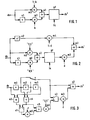
- the digital signals ds which are formed by means of an analog-digital converter (not shown in the figures) from a band-limited analog signal by means of a sampling signal of a constant sampling frequency, are fed to the first digital delay element v1, the delay v of which is equal to the sampling period.
- the digital signals delayed in this way are fed to the first multiplier m1 arranged at the output of the first delay element v1, which is also fed with the numerical value of the less than one part b of the sampling period by which the digital signals ds are also to be delayed.
- the first delay element v1 and the first multiplier m1 form the first parallel branch.
- the second multiplier m2 lies in the second parallel branch, on the one hand the factor 1-b and on the other hand the digital signals ds are supplied.
- the output of the first and second multiplier m1, m2 is at the first and second input of the first adder a1, the output of which is connected to the input of the digital peaking filter pf.
- the delayed digital signals ds' can be taken off at its output, and it compensates the amplitude frequency response of the subcircuit from the two parallel branches and the first adder a1 in the frequency range up to half the sampling frequency as precisely as possible.
- the amplitude frequency response of the subcircuit mentioned has a zero at half the sampling frequency.
- the delay circuit according to FIG. 1 has different behavior of the phase frequency response for different numerical values of the smaller one part b of the integer multiple, which property is undesirable in certain applications.
- This parallel branch of the arrangement according to FIG. 2 is associated with a further parallel branch, comparable to FIG. 1, which, seen from the input of the overall arrangement, initially contains the second delay element v2, the delay v 'of which is equal to that integral multiple of the sampling period 1, and which also contains the fourth multiplier m4 located at the output of the second delay element v2, to which the factor 1-d is supplied.
- the output of the third and fourth multiplier m3, m4 is at the first and second input of the second adder a2, at whose output the delayed digital signal ds' in turn occurs. If necessary, a further peaking filter can be arranged at the output of the second adder a2.
- the first, the second and the third delay stage vs1, vs2, vs3 are connected in series in terms of signal flow, each with the delay v, and the digital signal ds is fed to the first delay stage vs1 on the input side.
- This is also at the first input of the third adder a3 and its output at the first input of the fourth adder a4, to the second input of which the input of the third delay stage vs3 is connected, the output of which is at the input of the third adder a3.
- the output of the second subtractor s2 is connected via the third multiplier m3 to the first input of the second adder a2 and the output of the electronic switch s to its second input.
- the first input of the electronic switch s must be connected to its output, for 1.5.v to 2.v its second input must be connected to its output.
- the connecting lines between the individual subcircuits are only drawn in the form of lines, but in general the connections are buses, since parallel processing is common, in particular for fast signal processing.
- the individual subcircuits are also subcircuits suitable for such parallel processing, for example parallel adders, parallel multipliers etc.
- the delay circuit according to the invention can easily be implemented in the form of integrated circuits and in particular form part of a larger integrated circuit. Since this is r is a digital signal processing, is the realization by means of insulated gate field effect transistor circuits, that is by means of the so-called MOS technology, are particularly suitable. However, other concepts of integrated circuits are also possible.
Landscapes
- Engineering & Computer Science (AREA)
- Physics & Mathematics (AREA)
- General Physics & Mathematics (AREA)
- Data Mining & Analysis (AREA)
- Theoretical Computer Science (AREA)
- Pure & Applied Mathematics (AREA)
- Mathematical Analysis (AREA)
- Mathematical Optimization (AREA)
- Computational Mathematics (AREA)
- Mathematical Physics (AREA)
- Algebra (AREA)
- Software Systems (AREA)
- General Engineering & Computer Science (AREA)
- Databases & Information Systems (AREA)
- Analogue/Digital Conversion (AREA)
- Networks Using Active Elements (AREA)
- Filters That Use Time-Delay Elements (AREA)
Abstract
Description
- Die Erfindung betrifft eine Verzögerungsschaltung für Digitalsignale, die mittels eines von einem Abtastsignal konstanter Abtastfrequenz getakteten Analog-Digital-Wandlers aus einem bandbegrenzten Analogsignal gebildet sind und die um ein wählbares unganzzahliges Vielfaches der Abtastperiodendauer in einem vom Abtastsignal getakteten digitalen Schaltungssystem zu verzögern sind, vgl. den Oberbegriff des Anspruchs 1.
- Bei digitalen Schaltungssystemen, die Digitalsignale im Takt eines frequenzkonstanten Taktsignals verarbeiten, die wobei das Taktsignal identisch mit dem des Digitalsignale aus einem Analogsignal erzeugenden Analog-Digital-Wandlers sein kann, ist mit einfachen Mitteln als kleinstmögliche Verzögerungszeit nur die Abtastperiodendauer realisierbar. Sollen in einem solchen System kleinere Verzögerungszeiten als die Abtastperiodendauer oder ungeradzahlige Vielfache davon realisiert werden, welche Aufgabe sich beispielsweise bei der Interpolation von Digitalsignalen stellt, so sind die Digitalsignale mittels einer für diesen Zweck konzipierten Verzögerungsschaltung zu verzögern, wenn es sich verbietet, die Frequenz des Taktsignals zu erhöhen, um durch die dadurch kürzer werdende Abtastperiodendauer kürzere Verzögerungszeiten zu erzielen.
- Der in den Ansprüchen gekennzeichneten Erfindung liegt somit die Aufgabe zugrunde, für ein an einem festfrequenten Taktsignal betriebenes Schaltungssystem eine Verzögerungsschaltung für Digitalsignale anzugeben, die die Digitalsignale so beeinflußt, daß sie um ein unganzzahlig wählbares Vielfaches
- der Abtastperiodendauer verzögert erscheinen. Ferner sollen dabei sowohl der Amplituden- als auch der Phasenfrequenzgang der Verzögerungsschaltung optimal sein, wobei die gleichzeitige Optimierung beider Frequenzgänge im allgemeinen nur ausnahmsweise gelingen dürfte, jedoch je nach Anwendungsfall die Optimierung der einen unter Zurückstellung optimaler Bemessung der anderen im Sinne der Erfindung schon genügt.
- Die Erfindung wird nun anhand der Figuren der Zeichnung näher erläutert.
-
- Fig. 1 zeigt schematisch das Blockschaltbild eines Ausführungsbeispiels der Erfindung,
- Fig. 2 zeigt das Blockschaltbild eines Ausführungsbeispiels einer Weiterbildung der Erfindung,und
- Fig. 3 zeigt das Blockschaltbild eines speziellen Ausführungsbeispiels der Anordnung nach Fig. 2.
- Die Digitalsignale ds, die mittels eines in den Figuren nicht gezeigten Analog-Digital-Wandlers aus einem bandbegrenzten Analogsignal mittels eines Abtastsignals konstanter Abtastfrequenz gebildet sind, sind dem ersten digitalen Verzögerungsglied v1, dessen Verzögerung v gleich der Abtastperiodendauer ist, zugeführt. Die so verzögerten Digitalsignale sind dem am Ausgang des ersten Verzögerungsglieds v1 angeordneten ersten Multiplizierer m1 zugeführt, der auch mit dem Zahlenwert des Kleiner-Eins-Teils b der Abtastperiodendauer gespeist ist, um den die Digitalsignale ds auch verzögert werden sollen. Erstes Verzögerungsglied v1 und erster Multiplizierer m1 bilden den ersten Parallelzweig. Im zweiten Parallelzweig liegt der zweite Multiplizierer m2, dem einerseits der Faktor 1-b und andererseits die Digitalsignale ds zugeführt sind. Der Ausgang des ersten bzw. des zweiten Multiplizierers m1, m2 liegt am ersten bzw. zweiten Eingang des ersten Addierers a1, dessen Ausgang mit dem Eingang des digitalen Peaking-Filters pf verbunden ist. An dessen Ausgang sind die verzögerten Digitalsignale ds' abnehmbar,und es kompensiert den Amplitudenfrequenzgang der Teilschaltung aus den beiden Parallelzweigen und dem ersten Addierer a1 im Frequenzbereich bis zur halben Abtastfrequenz möglichst genau. Der Amplitudenfrequenzgang der erwähnten Teilschaltung hat nämlich bei der halben Abtastfrequenz eine Nullstelle.
- Die Verzögerungsschaltung nach Fig. 1 hat für unterschiedliche Zahlenwerte des Kleiner-Eins-Teils b des unganzzahligen Vielfachen unterschiedliches Verhalten des Phasenfrequenzganges, welche Eigenschaft in bestimmten Anwendungsfällen unerwünscht ist.
- Deshalb zeigt das Blockschaltbild nach Fig. 2 ein Ausführungsbeispiel einer weitergebildeten Verzögerungsschaltung. Im einzelnen ist eine Anordnung nach Fig. 1 für b = 0,5 verwendet, bei der am Ausgang des Peaking-Filters pf der dritte Multiplizierer m3 vorgesehen ist, dem der nunmehr mit d bezeichnete wählbare Teil der Abtastperiodendauer als zweites Eingangssignals zugeführt ist. Diesem einen Parallelzweig der Anordnung nach Fig. 2 ist in mit Fig. 1 vergleichbarer Weise ein weiterer Parallelzweig zugeordnet, der, vom Eingang der Gesamtanordnung aus gesehen, zunächst das zweite Verzögerungsglied v2 enthält, dessen Verzögerung v' gleich demjenigen ganzzahligen Vielfachen der Abtastperiodendauer ist, das das nächstniedere oder nächsthöhere zu der Gesamtverzögerung der Verzögerungsschaltung für b = 0,5 nach Fig. 1 ist, und der ferner den am Ausgang des zweiten Verzögerungsglieds v2 liegenden vierten Multiplizierer m4 enthält, dem der Faktor 1-d zugeführt ist. Der Ausgang des dritten bzw. des vierten Multiplizierers m3, m4 liegt am ersten bzw. zweiten Eingang des zweiten Addierers a2, an dessen Ausgang das verzögerte Digitalsignal ds' wiederum auftritt. Im Bedarfsfall kann am Ausgang des zweiten Addierers a2 ein weiteres Peaking-Filter angeordnet werden.
- Die Fig. 3 zeigt eine spezielle Ausführungsform der Anordnung nach Fig. 2 für ein einfaches Peaking-Filter mit der übertragungsfunktion H(z) = f+(1-2f)z-1+fz-2 wobei mit z bekanntlich die komplexe Frequenzvariable bezeichnet ist. In Fig. 3 sind die erste, die zweite und die dritte Verzögerungsstufe vs1, vs2, vs3 mit jeweils der Verzögerung v signalflußmäßig in Serie geschaltet, und der ersten Verzögerungsstufe vs1 ist das Digitalsignal ds eingangsseitig zugeführt. Dieses liegt auch am ersten Eingang des dritten Addierers a3 und deren Ausgang am ersten Eingang des vierten Addierers a4, mit dessen zweitem Eingang der Eingang der dritten Verzögerungsstufe vs3 verbunden ist, deren Ausgang am Eingang des dritten Addierers a3 liegt. Dessen Ausgang ist mit dem Minuendeingang und der Ausgang des vierten Addierers a4 mit dem Subtrahendeingang des ersten Subtrahierers s1 verbunden, dessen Ausgang über den fünften Multiplizierer m5 für den Peaking-Faktor f am ersten Eingang des fünften Addierers a5 angeschlossen ist, dessen zweiter Eingang am Ausgang des vierten Addierers a4 und dessen Ausgang über den ersten Multiplizierer m1 am Minuendeingang des zweiten Subtrahierers s2 liegt, an dessen Subtrahend- eingang der Ausgang des elektronischen Umschalters s angeschlossen ist. Dessen erster Eingang liegt am Ausgang der ersten Verzögerungsstufe vs1 und sein zweiter Eingang am Ausgang der zweiten Verzögerungsstufe vs2. Der Ausgang des zweiten Subtrahierers s2 ist über den dritten Multiplizierer m3 mit dem ersten Eingang des zweiten Addierers a2 und der Ausgang des elektronischen Umschalters s mit dessen zweitem Eingang verbunden. Für eine Gesamtverzögerung der Schaltung zwischen v und 1,5.v ist der erste Eingang des elektronischen Umschalters s mit dessen Ausgang, für 1,5.v bis 2.v ist dessen zweiter Eingang mit dessen Ausgang zu verbinden.
- Am Ausgang des ersten Multiplizierers m1 ergibt sich folgenden übertragungsfunktion 2 H' (z) = f +(z-1+z-2) (1-f) +z-3f. Es ist ersichtlich, daß die spezielle Ausführungsform der Fig. 3 eine bezüglich des Schaltungsaufwands minimisierte Anordnung ist, so daß einige der Teilschaltungen nach Fig. 2 in Fig. 3 real zwar nicht vorhanden, jedoch ihre Funktion von anderen Teilschaltungen der Fig. 3 übernommen sind.
- In den Figuren der Zeichnung sind der Übersichtlichkeit wegen die Verbindungsleitungen zwischen den einzelnen Teilschaltungen lediglich in Form von Strichen gezeichnet, im allgemeinen sind die Verbindungen jedoch Busse, da insbesondere für schnelle Signalverarbeitung parallele Verarbeitung üblich ist. In diesem Fall sind auch die einzelnen Teilschaltungen für solche Parallelverarbeitung geeignete Teilschaltungen, also beispielsweise Paralleladdierer, Parallelmultiplizierer etc.
- Die Verzögerungsschaltung nach der Erfindung kann ohne weiteres in Form integrierter Schaltungen realisiert werden und insbesondere einen Teil einer größeren integrierten Schaltung bilden. Da es sich umreine Digitalsignalverarbeitung handelt, ist die Realisierung mittels Isolierschicht-Feldeffekt-Transistorschaltungen, also mittels der sogenannten MOS-Technik,besonders geeignet. Aber auch andere Konzepte integrierter Schaltungen sind möglich.
Claims (4)
Priority Applications (5)
| Application Number | Priority Date | Filing Date | Title |
|---|---|---|---|
| EP84113894A EP0181953B1 (de) | 1984-11-16 | 1984-11-16 | Interpolator für Digitalsignale |
| DE8484113894T DE3484314D1 (de) | 1984-11-16 | 1984-11-16 | Interpolator fuer digitalsignale. |
| CN85107301A CN85107301A (zh) | 1984-11-16 | 1985-10-07 | 用于数字信号的延迟电路 |
| US06/795,081 US4760542A (en) | 1984-11-16 | 1985-11-05 | Delay circuit for digital signals |
| JP60256474A JPH0656942B2 (ja) | 1984-11-16 | 1985-11-15 | デジタル信号用遅延回路 |
Applications Claiming Priority (1)
| Application Number | Priority Date | Filing Date | Title |
|---|---|---|---|
| EP84113894A EP0181953B1 (de) | 1984-11-16 | 1984-11-16 | Interpolator für Digitalsignale |
Publications (2)
| Publication Number | Publication Date |
|---|---|
| EP0181953A1 true EP0181953A1 (de) | 1986-05-28 |
| EP0181953B1 EP0181953B1 (de) | 1991-03-20 |
Family
ID=8192289
Family Applications (1)
| Application Number | Title | Priority Date | Filing Date |
|---|---|---|---|
| EP84113894A Expired - Lifetime EP0181953B1 (de) | 1984-11-16 | 1984-11-16 | Interpolator für Digitalsignale |
Country Status (5)
| Country | Link |
|---|---|
| US (1) | US4760542A (de) |
| EP (1) | EP0181953B1 (de) |
| JP (1) | JPH0656942B2 (de) |
| CN (1) | CN85107301A (de) |
| DE (1) | DE3484314D1 (de) |
Cited By (5)
| Publication number | Priority date | Publication date | Assignee | Title |
|---|---|---|---|---|
| US4862271A (en) * | 1987-07-27 | 1989-08-29 | General Electric Company | Video signal interpolator with peaking |
| EP0262647A3 (en) * | 1986-09-30 | 1989-09-27 | Kabushiki Kaisha Toshiba | Sample rate conversion system having interpolation function |
| US5619270A (en) * | 1994-07-01 | 1997-04-08 | Harris Corp | Sample rate converter and sample rate conversion method |
| EP0847015A1 (de) | 1996-12-05 | 1998-06-10 | Micronas Intermetall GmbH | Digitale Filterkombination zur Interpolation |
| WO2010019418A2 (en) | 2008-08-15 | 2010-02-18 | M-I Llc | Centrifuge |
Families Citing this family (12)
| Publication number | Priority date | Publication date | Assignee | Title |
|---|---|---|---|---|
| ATE68643T1 (de) * | 1986-11-12 | 1991-11-15 | Siemens Ag | Mehrdimensionale (k-dimensionales) digitalfilter, das addierer, multiplizierer und schiebeglieder enthaelt. |
| US4823298A (en) * | 1987-05-11 | 1989-04-18 | Rca Licensing Corporation | Circuitry for approximating the control signal for a BTSC spectral expander |
| US5033018A (en) * | 1989-04-26 | 1991-07-16 | Hewlett-Packard Company | Filter and method for whitening digitally generated noise |
| US5041998A (en) * | 1989-11-30 | 1991-08-20 | The Grass Valley Group Inc. | Digital video mixer |
| US5359674A (en) * | 1991-12-11 | 1994-10-25 | David Sarnoff Research Center, Inc. | Pyramid processor integrated circuit |
| TW221083B (de) * | 1992-06-26 | 1994-02-11 | Philips Nv | |
| JP2526532B2 (ja) * | 1992-10-14 | 1996-08-21 | 日本プレシジョン・サーキッツ株式会社 | 画像処理用デジタルフィルタ |
| BE1007909A3 (nl) * | 1993-12-24 | 1995-11-14 | Philips Electronics Nv | Niet-geheeltallige vertraging. |
| US5553013A (en) * | 1994-09-30 | 1996-09-03 | Ford Motor Company | Delay generation filter |
| US5838600A (en) * | 1997-08-18 | 1998-11-17 | Thomson Consumer Electronics | DC gain invariant filter implementation |
| US6151682A (en) * | 1997-09-08 | 2000-11-21 | Sarnoff Corporation | Digital signal processing circuitry having integrated timing information |
| US6408322B1 (en) | 1999-02-17 | 2002-06-18 | Thomson Licensing S.A. | Apparatus and method for anchoring predetermined points of the impulse frequency response of a physically-realized filter |
Citations (5)
| Publication number | Priority date | Publication date | Assignee | Title |
|---|---|---|---|---|
| US3943346A (en) * | 1974-07-22 | 1976-03-09 | Rca Corporation | Digital interpolator for reducing time quantization errors |
| US4074308A (en) * | 1976-10-28 | 1978-02-14 | Rca Corporation | Delay line network for processing a composite electrical signal |
| EP0022642A1 (de) * | 1979-07-12 | 1981-01-21 | The Rank Organisation Limited | Signalverarbeitungsvorrichtung für Bildabtaster |
| GB2078406A (en) * | 1980-06-10 | 1982-01-06 | Western Electric Co | Interpolator |
| US4472785A (en) * | 1980-10-13 | 1984-09-18 | Victor Company Of Japan, Ltd. | Sampling frequency converter |
Family Cites Families (7)
| Publication number | Priority date | Publication date | Assignee | Title |
|---|---|---|---|---|
| US3521042A (en) * | 1967-07-19 | 1970-07-21 | Ibm | Simplified digital filter |
| US4044241A (en) * | 1972-01-12 | 1977-08-23 | Esl Incorporated | Adaptive matched digital filter |
| JPS5765918A (en) * | 1980-10-13 | 1982-04-21 | Victor Co Of Japan Ltd | Sampling frequency converter |
| NL8201533A (nl) * | 1982-04-13 | 1983-11-01 | Philips Nv | Een zender ingericht voor het zenden van fm gemoduleerde signalen. |
| JPS5952911A (ja) * | 1982-09-20 | 1984-03-27 | Nec Corp | トランスバ−サル・フイルタ |
| DE3276292D1 (en) * | 1982-10-06 | 1987-06-11 | Itt Ind Gmbh Deutsche | Digital filter integrated circuit for the chrominance channel of a colour television apparatus |
| US4542475A (en) * | 1982-11-23 | 1985-09-17 | Rca Corporation | Sampled data filter system as for a digital TV |
-
1984
- 1984-11-16 DE DE8484113894T patent/DE3484314D1/de not_active Expired - Fee Related
- 1984-11-16 EP EP84113894A patent/EP0181953B1/de not_active Expired - Lifetime
-
1985
- 1985-10-07 CN CN85107301A patent/CN85107301A/zh active Pending
- 1985-11-05 US US06/795,081 patent/US4760542A/en not_active Expired - Fee Related
- 1985-11-15 JP JP60256474A patent/JPH0656942B2/ja not_active Expired - Lifetime
Patent Citations (5)
| Publication number | Priority date | Publication date | Assignee | Title |
|---|---|---|---|---|
| US3943346A (en) * | 1974-07-22 | 1976-03-09 | Rca Corporation | Digital interpolator for reducing time quantization errors |
| US4074308A (en) * | 1976-10-28 | 1978-02-14 | Rca Corporation | Delay line network for processing a composite electrical signal |
| EP0022642A1 (de) * | 1979-07-12 | 1981-01-21 | The Rank Organisation Limited | Signalverarbeitungsvorrichtung für Bildabtaster |
| GB2078406A (en) * | 1980-06-10 | 1982-01-06 | Western Electric Co | Interpolator |
| US4472785A (en) * | 1980-10-13 | 1984-09-18 | Victor Company Of Japan, Ltd. | Sampling frequency converter |
Non-Patent Citations (1)
| Title |
|---|
| JOURNAL OF THE SOCIETY OF MOTION PICTURE AND TELEVISION ENGINEERS, Band 84, Nr. 7, Juli 1975, Seiten 545-551, Scardale, N.Y., US; J.P. ROSSI: "Digital television image enhancement" * |
Cited By (6)
| Publication number | Priority date | Publication date | Assignee | Title |
|---|---|---|---|---|
| EP0262647A3 (en) * | 1986-09-30 | 1989-09-27 | Kabushiki Kaisha Toshiba | Sample rate conversion system having interpolation function |
| US4862271A (en) * | 1987-07-27 | 1989-08-29 | General Electric Company | Video signal interpolator with peaking |
| US5619270A (en) * | 1994-07-01 | 1997-04-08 | Harris Corp | Sample rate converter and sample rate conversion method |
| DE4423224C2 (de) * | 1994-07-01 | 1998-02-26 | Harris Corp | Videosignal-Dekoder und Verfahren zur Dekodierung von Videosignalen |
| EP0847015A1 (de) | 1996-12-05 | 1998-06-10 | Micronas Intermetall GmbH | Digitale Filterkombination zur Interpolation |
| WO2010019418A2 (en) | 2008-08-15 | 2010-02-18 | M-I Llc | Centrifuge |
Also Published As
| Publication number | Publication date |
|---|---|
| US4760542A (en) | 1988-07-26 |
| CN85107301A (zh) | 1986-07-09 |
| JPH0656942B2 (ja) | 1994-07-27 |
| JPS61126812A (ja) | 1986-06-14 |
| EP0181953B1 (de) | 1991-03-20 |
| DE3484314D1 (de) | 1991-04-25 |
Similar Documents
| Publication | Publication Date | Title |
|---|---|---|
| EP0181953B1 (de) | Interpolator für Digitalsignale | |
| DE3851053T2 (de) | Fir digitale filteranordnung. | |
| DE3855437T2 (de) | Abtastfrequenzumsetzer zum Umsetzen einer niedrigen Abtastfrequenz in eine höhere Abtastfrequenz und Verfahren dafür | |
| EP0149785A1 (de) | Verfahren und Schaltungsanordnung zur Digitalsignalverarbeitung nach Art eines vorzugsweise adaptiven Transversalfilters | |
| EP0305708B1 (de) | Digitales Dezimierungsfilter | |
| EP0099142A2 (de) | Verfahren und Anordnung zum Demodulieren eines frequenzmodulierten Eingangssignals | |
| DE69623871T2 (de) | Hardwareeffizientes Interpolationsfilter | |
| DE2517230C2 (de) | Impulsgenerator | |
| DE2302298B2 (de) | Hilbertumsetzer | |
| EP0146652B1 (de) | Digitaler FM-Demodulator für digitalisierte FM-Signale | |
| EP1282940A1 (de) | Stromspiegel und verfahren zum betreiben eines stromspiegels | |
| DE3922469C2 (de) | ||
| DE3751088T2 (de) | Signalverarbeitungseinrichtung. | |
| DE2456245C2 (de) | Schaltungsanordnung für ein digitales Filter | |
| EP0106000B1 (de) | Digitalschaltung zur Unterdrückung von Änderungen eines Digitalsignals | |
| DE2011772A1 (de) | Filter mit einer periodischen übertragungscharakteristik | |
| EP0192788B1 (de) | Integrierte digitale Frequenzdemodulationsteilschaltung | |
| DE69223166T2 (de) | Eingangs-gewichtetes Transversalfilter | |
| EP0197165A1 (de) | Datenreduzierschaltung für digitale Videosignale mit einem Differenz-Pulscodemodulator | |
| DE3302550C2 (de) | ||
| EP0445335A1 (de) | Vorrichtung und Verfahren zur Erhöhung der Taktrate eines FIR-Filters | |
| DE69223269T2 (de) | Zyklisches digitales Filter | |
| DE4135335C2 (de) | Einrichtung zur Gewinnung zweier in Quadraturphasenbeziehung stehender Signale aus einem digitalen Signal | |
| EP0255554B1 (de) | Nichtrekursives Digitalfilter | |
| DE4109212C2 (de) | Adaptives Digitalfilter |
Legal Events
| Date | Code | Title | Description |
|---|---|---|---|
| PUAI | Public reference made under article 153(3) epc to a published international application that has entered the european phase |
Free format text: ORIGINAL CODE: 0009012 |
|
| AK | Designated contracting states |
Kind code of ref document: A1 Designated state(s): DE FR GB IT NL |
|
| 17P | Request for examination filed |
Effective date: 19861121 |
|
| 17Q | First examination report despatched |
Effective date: 19890620 |
|
| GRAA | (expected) grant |
Free format text: ORIGINAL CODE: 0009210 |
|
| AK | Designated contracting states |
Kind code of ref document: B1 Designated state(s): DE FR GB IT NL |
|
| GBT | Gb: translation of ep patent filed (gb section 77(6)(a)/1977) | ||
| REF | Corresponds to: |
Ref document number: 3484314 Country of ref document: DE Date of ref document: 19910425 |
|
| ET | Fr: translation filed | ||
| ITF | It: translation for a ep patent filed | ||
| PLBE | No opposition filed within time limit |
Free format text: ORIGINAL CODE: 0009261 |
|
| STAA | Information on the status of an ep patent application or granted ep patent |
Free format text: STATUS: NO OPPOSITION FILED WITHIN TIME LIMIT |
|
| 26N | No opposition filed | ||
| PGFP | Annual fee paid to national office [announced via postgrant information from national office to epo] |
Ref country code: FR Payment date: 19961021 Year of fee payment: 13 |
|
| PGFP | Annual fee paid to national office [announced via postgrant information from national office to epo] |
Ref country code: NL Payment date: 19961024 Year of fee payment: 13 |
|
| PGFP | Annual fee paid to national office [announced via postgrant information from national office to epo] |
Ref country code: GB Payment date: 19961025 Year of fee payment: 13 |
|
| PG25 | Lapsed in a contracting state [announced via postgrant information from national office to epo] |
Ref country code: GB Free format text: LAPSE BECAUSE OF NON-PAYMENT OF DUE FEES Effective date: 19971116 |
|
| PG25 | Lapsed in a contracting state [announced via postgrant information from national office to epo] |
Ref country code: FR Free format text: THE PATENT HAS BEEN ANNULLED BY A DECISION OF A NATIONAL AUTHORITY Effective date: 19971130 |
|
| PG25 | Lapsed in a contracting state [announced via postgrant information from national office to epo] |
Ref country code: NL Free format text: LAPSE BECAUSE OF NON-PAYMENT OF DUE FEES Effective date: 19980601 |
|
| GBPC | Gb: european patent ceased through non-payment of renewal fee |
Effective date: 19971116 |
|
| NLV4 | Nl: lapsed or anulled due to non-payment of the annual fee |
Effective date: 19980601 |
|
| REG | Reference to a national code |
Ref country code: FR Ref legal event code: ST |
|
| PGFP | Annual fee paid to national office [announced via postgrant information from national office to epo] |
Ref country code: DE Payment date: 20021202 Year of fee payment: 19 |
|
| PG25 | Lapsed in a contracting state [announced via postgrant information from national office to epo] |
Ref country code: DE Free format text: LAPSE BECAUSE OF NON-PAYMENT OF DUE FEES Effective date: 20040602 |