EP0182068A2 - Condensateur pour le montage en surface - Google Patents
Condensateur pour le montage en surface Download PDFInfo
- Publication number
- EP0182068A2 EP0182068A2 EP85112760A EP85112760A EP0182068A2 EP 0182068 A2 EP0182068 A2 EP 0182068A2 EP 85112760 A EP85112760 A EP 85112760A EP 85112760 A EP85112760 A EP 85112760A EP 0182068 A2 EP0182068 A2 EP 0182068A2
- Authority
- EP
- European Patent Office
- Prior art keywords
- sheath
- capacitor
- capacitor according
- connection
- round
- Prior art date
- Legal status (The legal status is an assumption and is not a legal conclusion. Google has not performed a legal analysis and makes no representation as to the accuracy of the status listed.)
- Withdrawn
Links
Images

Classifications
-
- H—ELECTRICITY
- H01—ELECTRIC ELEMENTS
- H01G—CAPACITORS; CAPACITORS, RECTIFIERS, DETECTORS, SWITCHING DEVICES, LIGHT-SENSITIVE OR TEMPERATURE-SENSITIVE DEVICES OF THE ELECTROLYTIC TYPE
- H01G2/00—Details of capacitors not covered by a single one of groups H01G4/00-H01G11/00
- H01G2/02—Mountings
- H01G2/06—Mountings specially adapted for mounting on a printed-circuit support
- H01G2/065—Mountings specially adapted for mounting on a printed-circuit support for surface mounting, e.g. chip capacitors
-
- H—ELECTRICITY
- H01—ELECTRIC ELEMENTS
- H01G—CAPACITORS; CAPACITORS, RECTIFIERS, DETECTORS, SWITCHING DEVICES, LIGHT-SENSITIVE OR TEMPERATURE-SENSITIVE DEVICES OF THE ELECTROLYTIC TYPE
- H01G9/00—Electrolytic capacitors, rectifiers, detectors, switching devices, light-sensitive or temperature-sensitive devices; Processes of their manufacture
- H01G9/004—Details
- H01G9/008—Terminals
- H01G9/012—Terminals specially adapted for solid capacitors
-
- H—ELECTRICITY
- H05—ELECTRIC TECHNIQUES NOT OTHERWISE PROVIDED FOR
- H05K—PRINTED CIRCUITS; CASINGS OR CONSTRUCTIONAL DETAILS OF ELECTRIC APPARATUS; MANUFACTURE OF ASSEMBLAGES OF ELECTRICAL COMPONENTS
- H05K3/00—Apparatus or processes for manufacturing printed circuits
- H05K3/30—Assembling printed circuits with electric components, e.g. with resistors
- H05K3/32—Assembling printed circuits with electric components, e.g. with resistors electrically connecting electric components or wires to printed circuits
- H05K3/34—Assembling printed circuits with electric components, e.g. with resistors electrically connecting electric components or wires to printed circuits by soldering
- H05K3/341—Surface mounted components
- H05K3/3421—Leaded components
- H05K3/3426—Leaded components characterised by the leads
-
- Y—GENERAL TAGGING OF NEW TECHNOLOGICAL DEVELOPMENTS; GENERAL TAGGING OF CROSS-SECTIONAL TECHNOLOGIES SPANNING OVER SEVERAL SECTIONS OF THE IPC; TECHNICAL SUBJECTS COVERED BY FORMER USPC CROSS-REFERENCE ART COLLECTIONS [XRACs] AND DIGESTS
- Y02—TECHNOLOGIES OR APPLICATIONS FOR MITIGATION OR ADAPTATION AGAINST CLIMATE CHANGE
- Y02P—CLIMATE CHANGE MITIGATION TECHNOLOGIES IN THE PRODUCTION OR PROCESSING OF GOODS
- Y02P70/00—Climate change mitigation technologies in the production process for final industrial or consumer products
- Y02P70/50—Manufacturing or production processes characterised by the final manufactured product
Definitions
- the invention relates to a capacitor, in particular for surface mounting by reflow or wave soldering, consisting of a capacitor body provided with a jacket with opposing connection elements emerging from the jacket in the form of double connections. '
- Capacitors of this type are known from DE-PS 31 34 617.
- the connection elements of these known film capacitors consist of single or double webs soldered to the respective end connection layer, which are angled at a distance from the capacitor body perpendicular to the end connection layer to the capacitor body, each web transitioning into a wide contact area at the bending point.
- Tantalum capacitors with two connections as well as with more than two connections are also known; it is also known to design such tantalum capacitors in chip form, so that there are elements comparable to IC packages which can be used as pluggable elements when using flat contacts.
- the object of the invention is to produce capacitors of the type defined at the outset in a particularly economical manner with a high degree of dimensional accuracy and to enable particularly reliable automatic contacting, these capacitors also being insensitive to the heat exposure occurring during contacting and having to have optimum electrical values.
- connection elements are designed as round wires, that the round wire sections projecting over the sheath are pressed to flat wire sections, and that each flat pressed wire section has at least one essentially right-angled bend.
- the use of round wires enables particularly economical production on the one hand and surprisingly advantageous electrical properties on the other hand.
- the provided covering ensures an exact positioning of the connection elements, and the flat wire sections produced after the formation of the covering enable, on the one hand, automatic assembly analogous to IC housings and protect. on the other hand, the capacitor body before possibly dangerous heat exposure.
- the use of round wires that run from rolls means that there are no torsion or twisting problems during production, and the soldering process can be un going to be problematic.
- the respective capacitor body level already specifies the crimp level for further processing, ie it can be squeezed without problems in a precisely aligned manner.
- the flat-pressed wire sections can be bent very close to the capacitor body, the flat-squeezed sections come directly to the capacitor body, as a result of which the inductance is reduced and the cutoff frequency is increased, which opens up additional areas of application for the component.
- connection elements which are stamped from sheet metal, any loss of material is also avoided by the invention and the expensive stamping process is superfluous.
- capacitor body 1 shows in a schematic manner a capacitor body 1 which can be constructed, for example, from aluminum and dielectric foils or from metallized foils, in particular also in a layered construction.
- this capacitor body 1 is provided with connection layers 2, which are preferably applied by looping.
- Fig. 2 shows a view substantially corresponding to the representation in Fig. 1, however, U-shaped wire connections 3 are used as connecting round wires, and the narrow middle part of the U-shaped connecting element with the looped end face of the capacitor, in which it is preferably a metallized film capacitor, is electrically connected, by soldering or welding.
- the opposite, parallel routing of the connecting wires 3 from the sheath, which is also not shown in FIG. 2, has proven to be particularly advantageous with regard to assembly and electrical values.
- the U-shaped connection element which is assigned to each end face of the capacitor can be symmetrical, i.e. be formed with legs of equal length, but it is also 'for some applications favorable to choose one leg shorter than the other, in particular half as long.
- the side view according to FIG. 3 and the top view according to FIG. 4 show the capacitor explained with reference to FIG. 2 after applying a sheath 4.
- This sheath 4 has a cuboid shape and is preferably realized by pressing, casting or by installing the capacitor body in a cup .
- the covering consists in particular of epoxy, polyester or silicone resin, in a flame-retardant setting.
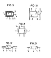
- FIG. 5 shows a finished capacitor according to the invention, in which the round connecting wires are pressed flat immediately after they emerge from the sheathing 4, so that flat wire sections 5 are formed.
- these flat wire sections 5 run parallel to the side faces of the cuboid Sheathing, since a 90 0 kink 6 is provided in the area of the transition from the round wire section to the flat wire section.
- the connecting wires are cut so that there is a maximum protrusion of 0.5 mm.
- the flat wire portions 5 are guided substantially parallel to the end walls of the body 4 to the lower edge thereof and bent there again to kinks 7 90 0 outwards.
- the free end portions of the flat wire portions 5 are not bent outward but inward by about 90 ° and grip under the body 4 a little, the free end portion of the F laughing wire areas again approximately parallel to the bottom of the capacitor body extends. ;
- FIG. 8 shows a preferred possibility for producing the capacitors according to the invention, wherein a carrier form with frame elements 8 on both sides made of strip material is used, on which the U-shaped connecting wires 3 are welded inward, with such mutual spacing of the mutually opposite connecting wires, that the capacitor body can be inserted and soldered or welded appropriately, whereby a continuous manufacturing process is possible.
- Fig. 9 shows the basic structure of a tantalum capacitor body 1, consisting of a tantalum anode 9 with an electrolytically generated oxide layer as a dielectric, a counter electrode 10 made of a semiconductor, for example made of rIn0 2 , a graphite layer 11, and layers 12, 13 made of silver, solder or conductive casting resin, wherein the outer layer 13 forms the anode bottom.
- the positive connection element 14 consists of a tantalum wire sintered into the tantalum anode 9.
- a round wire 15 is welded at right angles to the positive connecting element 14, the length of this round wire 15 being selected such that a protrusion on both sides is produced with respect to the tantalum body 1.
- a round wire 16 is soldered to the anode bottom 13 as a negative connection.
- the two round wires 15, 16 are preferably in a plane parallel to the longitudinal axis of the tantalum body 1.
- a weld 17 between the connecting element 14 and the round wire 15 is at a clear distance from the tantalum body 1. This distance corresponds to at least half the width of the tantalum body. !
- FIG. 11 shows the arrangement according to FIG. 10 after the covering 4 has been applied.
- This covering can be applied by pressing, casting and the like, and it preferably has a cuboid shape.
- the sections of the round wires located within the covering are clearly positioned in their position by the covering.
- FIG. 1 A variant of the possible contacting is shown in FIG.
- FIG. 5 shows a side view of the arrangement according to FIG. 12 after the covering 11 has been applied.
- each with four connections, two cathode and two anode connection wires are preferably further developed for use as chip capacitors for surface mounting on substrates in the manner explained with reference to FIGS. 6 and 7, ie the corresponding flat wire sections are formed and these flat wire sections are angled in the ways also explained. The advantages already explained are again obtained.
- the capacitors described allow an extreme! economical production, provide exact dimensional accuracy and are ideally suited for automatic assembly, whereby the interplay of round wire sections and flat wire sections has a favorable manufacturing effect and, above all, leads to an increase in functional reliability due to the formation of heat barriers with regard to the thermal stress that occurs during soldering.
Landscapes
- Engineering & Computer Science (AREA)
- Power Engineering (AREA)
- Microelectronics & Electronic Packaging (AREA)
- Manufacturing & Machinery (AREA)
- Fixed Capacitors And Capacitor Manufacturing Machines (AREA)
Applications Claiming Priority (4)
| Application Number | Priority Date | Filing Date | Title |
|---|---|---|---|
| DE3436900 | 1984-10-08 | ||
| DE19843436900 DE3436900A1 (de) | 1984-10-08 | 1984-10-08 | Tantal-kondensator |
| DE3436898 | 1984-10-08 | ||
| DE19843436898 DE3436898A1 (de) | 1984-10-08 | 1984-10-08 | Folien-chip-kondensator |
Publications (2)
| Publication Number | Publication Date |
|---|---|
| EP0182068A2 true EP0182068A2 (fr) | 1986-05-28 |
| EP0182068A3 EP0182068A3 (fr) | 1987-02-04 |
Family
ID=25825475
Family Applications (1)
| Application Number | Title | Priority Date | Filing Date |
|---|---|---|---|
| EP85112760A Withdrawn EP0182068A3 (fr) | 1984-10-08 | 1985-10-08 | Condensateur pour le montage en surface |
Country Status (1)
| Country | Link |
|---|---|
| EP (1) | EP0182068A3 (fr) |
Cited By (3)
| Publication number | Priority date | Publication date | Assignee | Title |
|---|---|---|---|---|
| EP0222547A1 (fr) * | 1985-10-31 | 1987-05-20 | Integrated Power Components | Condensateur enroulé |
| EP0389678A1 (fr) * | 1989-03-29 | 1990-10-03 | American Precision Industries Inc | Procédé de fabrication d'un composant électrique montable en surface |
| DE4114391A1 (de) * | 1991-05-03 | 1992-11-05 | Hohenloher Spulenkoerper | Oberflaechenmontierbares elektronisches bauelement und verfahren zu seiner herstellung |
Family Cites Families (5)
| Publication number | Priority date | Publication date | Assignee | Title |
|---|---|---|---|---|
| GB968989A (fr) * | ||||
| DE828414C (de) * | 1949-10-11 | 1952-01-17 | Steatit Magnesia Ag | Anordnung zur Halterung und zum Stromanschluss von rohrfoermigen elektrischen Schaltelementen |
| GB1345135A (en) * | 1971-12-21 | 1974-01-30 | Int Standard Electric Corp | Capacitor |
| US4001656A (en) * | 1974-12-27 | 1977-01-04 | P. R. Mallory & Co., Inc. | Capacitor having a plurality of anode risers for low impedance at high frequency |
| DE3134617C2 (de) * | 1981-09-01 | 1989-11-02 | Ernst Roederstein Spezialfabrik für Kondensatoren GmbH, 8300 Landshut | Folien-Kondensator |
-
1985
- 1985-10-08 EP EP85112760A patent/EP0182068A3/fr not_active Withdrawn
Cited By (3)
| Publication number | Priority date | Publication date | Assignee | Title |
|---|---|---|---|---|
| EP0222547A1 (fr) * | 1985-10-31 | 1987-05-20 | Integrated Power Components | Condensateur enroulé |
| EP0389678A1 (fr) * | 1989-03-29 | 1990-10-03 | American Precision Industries Inc | Procédé de fabrication d'un composant électrique montable en surface |
| DE4114391A1 (de) * | 1991-05-03 | 1992-11-05 | Hohenloher Spulenkoerper | Oberflaechenmontierbares elektronisches bauelement und verfahren zu seiner herstellung |
Also Published As
| Publication number | Publication date |
|---|---|
| EP0182068A3 (fr) | 1987-02-04 |
Similar Documents
| Publication | Publication Date | Title |
|---|---|---|
| DE69930785T2 (de) | Festelektrolytkondensator in Chip-Bauweise und dessen Herstellungsverfahren | |
| DE68920185T2 (de) | Vorrichtung zur Verbindung von elektrischen Drähten mit Leiterdrähten. | |
| DE3329886C2 (de) | Verfahren zum Herstellen von Trocken-Elektrolyt-Kondensatoren | |
| DE102007016692B3 (de) | Metall-Fixiermaterial-Durchführung | |
| DE19830820A1 (de) | Elektronisches Keramikbauteil und Verfahren zum Herstellen des elektronischen Keramikbauteils | |
| DE102014104399B4 (de) | Halbleiterchipgehäuse umfassend einen Leadframe | |
| DE19928788A1 (de) | Elektronische Keramikkomponente | |
| DE19640849C2 (de) | Schmelzgesicherter, oberflächenbefestigbarer Trockenelektrolytkondensator | |
| DE19714544B4 (de) | Verfahren zum Anbringen eines Trockenelektrolytkondensators auf einer Leiterplatine und Anordnung des Kondensators und der Platine | |
| DE4015463C2 (de) | Verfahren zum Anbringen einer Mehrzahl von Anschlußschichten auf der Außenseite eines Keramik-Bauelements und keramischer Mehrschichtenkondensator | |
| DE4423561C2 (de) | Oberflächenmontage-Elektronikbauteil mit Schmelzsicherung und entsprechendes Herstellungsverfahren | |
| DE19928787A1 (de) | Drahteinlageinduktor und Verfahren zum Herstellen desselben | |
| DE112016002171T5 (de) | Anschluss zur leitungsverbindung und verfahren zur verbindung des anschlusses mit der leitung | |
| DE3036913A1 (de) | Induktivitaetseinrichtung | |
| DE102018209534A1 (de) | Spulenkomponente und Herstellungsverfahren derselben | |
| DE19620087B4 (de) | Verfahren zum Herstellen eines bausteinartigen, gesicherten Kondensators mit Festelektrolyt | |
| DE19523977A1 (de) | Microchip-Sicherung | |
| DE3432670C2 (fr) | ||
| DE10131469B4 (de) | Festkörperelektrolytkondensator mit einem verbesserten Anodenanschluss | |
| EP0133883A1 (fr) | Connecteur pour soudage par ultrasons | |
| EP0182068A2 (fr) | Condensateur pour le montage en surface | |
| DE3625238C2 (fr) | ||
| DE9407550U1 (de) | Elektrische Sicherung | |
| EP0171838A1 (fr) | Composant électrique encapsule | |
| DE1916554B2 (de) | Verfahren zum Herstellen von Halbleitergleichrichteranordnungen |
Legal Events
| Date | Code | Title | Description |
|---|---|---|---|
| PUAI | Public reference made under article 153(3) epc to a published international application that has entered the european phase |
Free format text: ORIGINAL CODE: 0009012 |
|
| AK | Designated contracting states |
Kind code of ref document: A2 Designated state(s): BE CH DE FR GB IT LI NL SE |
|
| PUAL | Search report despatched |
Free format text: ORIGINAL CODE: 0009013 |
|
| AK | Designated contracting states |
Kind code of ref document: A3 Designated state(s): BE CH DE FR GB IT LI NL SE |
|
| STAA | Information on the status of an ep patent application or granted ep patent |
Free format text: STATUS: THE APPLICATION HAS BEEN WITHDRAWN |
|
| 18W | Application withdrawn |
Withdrawal date: 19870128 |
|
| RIN1 | Information on inventor provided before grant (corrected) |
Inventor name: PETRICK, PAUL, DR. |