EP0182087A1 - Circuit pour la détection de collisions - Google Patents
Circuit pour la détection de collisions Download PDFInfo
- Publication number
- EP0182087A1 EP0182087A1 EP85113021A EP85113021A EP0182087A1 EP 0182087 A1 EP0182087 A1 EP 0182087A1 EP 85113021 A EP85113021 A EP 85113021A EP 85113021 A EP85113021 A EP 85113021A EP 0182087 A1 EP0182087 A1 EP 0182087A1
- Authority
- EP
- European Patent Office
- Prior art keywords
- signal
- signal state
- bus line
- line system
- low
- Prior art date
- Legal status (The legal status is an assumption and is not a legal conclusion. Google has not performed a legal analysis and makes no representation as to the accuracy of the status listed.)
- Granted
Links
- 238000001514 detection method Methods 0.000 title claims abstract description 10
- 239000004020 conductor Substances 0.000 claims abstract description 18
- 230000007704 transition Effects 0.000 claims abstract description 5
- 230000005540 biological transmission Effects 0.000 claims description 24
- 230000001934 delay Effects 0.000 description 2
- 238000000034 method Methods 0.000 description 2
- 101100172132 Mus musculus Eif3a gene Proteins 0.000 description 1
- 230000008030 elimination Effects 0.000 description 1
- 238000003379 elimination reaction Methods 0.000 description 1
Images
Classifications
-
- H—ELECTRICITY
- H04—ELECTRIC COMMUNICATION TECHNIQUE
- H04L—TRANSMISSION OF DIGITAL INFORMATION, e.g. TELEGRAPHIC COMMUNICATION
- H04L12/00—Data switching networks
- H04L12/28—Data switching networks characterised by path configuration, e.g. LAN [Local Area Networks] or WAN [Wide Area Networks]
- H04L12/40—Bus networks
- H04L12/407—Bus networks with decentralised control
- H04L12/413—Bus networks with decentralised control with random access, e.g. carrier-sense multiple-access with collision detection [CSMA-CD]
- H04L12/4135—Bus networks with decentralised control with random access, e.g. carrier-sense multiple-access with collision detection [CSMA-CD] using bit-wise arbitration
Definitions
- bus line systems are often used, in which the respectively connected stations have optional access via transmitting and receiving devices (Random Access) to the bus line system.
- the digital signals emitted by a station are transmitted on both sides of the bus and are only picked up by the subscriber station (s) designated by the address (es) in accordance with the preceding addresses.
- CSMA / CD Carrier Sense Multiplex Access with Collision Oetection
- the station in question begins to transmit, initially "listening" until it is certain after a certain period of time (round trip delay time) that all the other stations have noticed their transmission. If another station has started to transmit at about the same time, both stations become one Detect their digital signals collide with those of the other station, whereupon they abort their transmission process in order to start again after a random period of time.
- the multiple transmission can be detected on the basis of a level increase occurring on the bus line system due to the addition of two signals, which, however, requires a relatively complex analog technology, in particular in the form of very precise symmetrical operational amplifiers (to be fed with two voltages).
- a simple method with which a multiple transmission can be recognized is that the active station compares the signal it is currently emitting (and emitted) with the signal state prevailing at its receiving device on the bus line system, one signal then distinguishing one Indicates collision.
- the detection of such a signal (state) difference presupposes that one signal state always asserts itself physically on the bus line system over the other signal state (in the case of binary signals).
- the detection can then take place in such a way that the transmission and reception signal states are scanned cyclically and then compared with one another, which is, however, associated with time gaps, on the basis of which an occurred collision and the like. May not be recognized.
- the object of the invention is to enable collision detection when a subscriber station accesses a bus line system using simple means and at the same time quickly and with high security.
- the invention relates to a circuit arrangement for collision detection when a subscriber station accesses a bus line system, to which the receiving devices and the two signal states, one of which forms a dominance signal state which prevails over the other signal state on the bus line system, are connected to 'transmitting devices of such subscriber stations Comparison of the transmission signal state just given in the subscriber station with the signal state currently prevailing on the bus line system, in particular bus system with two signal conductors and a line shield (ground); According to the invention, this circuit arrangement is characterized in that it detects an access collision in its transmitting device on the basis of a signal transition on the bus line system into the dominance signal state while the other signal state is ongoing.
- the invention which enables seamless collision detection in the context of a signal state comparison, can be designed such that an edge-controlled bistable flip-flop is provided, the set input of which is connected to a line of the subscriber station carrying the respective transmission signal, from the receiving device of which the clock input of the edge-controlled bistable is provided Tilting element is acted upon by a signal corresponding to the signal state given in each case on the bus line system.
- this known telecommunication system with the elimination of an otherwise given dominance of said one signal state caused by the increase in resistance, has a different path than the invention.
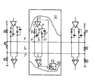
- a bus line system can preferably be formed by a shielded (twisted pair) cable having two twisted wires with a characteristic impedance of, for example, 150 ohms, the two twisted wires forming the signal conductors 1 'shown in the drawing, 1 "form.
- Transmitter devices S are connected to the two signal conductors 1 ', 1 "via two differential outputs s', s"; these transmitting devices S, together with receiving devices E also connected to the two signal conductors 1 ', 1 "via differential inputs +, - each belong to a subscriber station St, which is not shown in any more detail, for example a telecommunication terminal, a computer or a switching processor.
- the transmitting devices S each have a bus transmitter T provided with two differential outputs t ', t ", which is a tristate bus transmitter, for example of the type AM26LS31 (AMD) or SN74ALS1631 (TI) or can also be a bus transmitter of no such third state, for example of the type 9638 (Fairchild).
- the transmission devices S have two possible signal states, the signal state (given at a transmission device S) (e.g. a signal state LOW) being different from the signal state (given at another transmission device) (the signal state HIGH in the example) in the bus line system L. enforced, ie causes a dominance signal state in the transmission system.
- the transmission device S in question leaves the two signal conductors 1 1 , 1 "- and thus also the subscriber stations connected to them - at least approximately unloaded.
- each with a two differential outputs t ', t "having bus transmitters T formed transmission devices S which connect the two differential outputs t', t" to the two signal conductors 1 ', 1 "via two diodes D', D" in the mentioned other signal state (HIGH in the off state).
- these diodes which have a low forward voltage and a low forward resistance, switch the potentials occurring at the two bus transmitter outputs t 'and t "having a low internal resistance practically unchanged to the two signal conductors 1' and 1 "by, sc that there in the mentioned one signal state (LOW)
- the transmitting device S under consideration is in its other signal state (HIGH), in which a bus transmission potential of approximately 3.7 V in the example and a bus transmission potential of approximately 0.1 V occurs in the example at the bus transmitter output t 'and prevail nevertheless from another bus transmitter the previously specified potential ratios on the two signal conductors 1 'and 1 ", the two diodes D' and D" of the transmitter S under consideration are blocked, and now each have one at their two signal outputs s' and s " compared with the one signal state given in the case of diodes in the on state low internal resistance, large internal resistance, transmission device S leaves the two signal conductors 1 1 , 1 "practically unloaded, in other words, the transmission device S and the signal conductors 1 ', 1" are practically decoupled from one another.
- HIGH a bus transmission potential of approximately 3.7 V in the example and a bus transmission potential of approximately 0.1 V occurs in the example at the bus transmitter output t 'and prevail nevertheless from another bus transmitter the previously specified potential ratios on the
- the two signal conductors 1 ', 1 are connected to at least one voltage divider U-R1-R2-R3 ground, the internal resistance (R2
- this voltage divider lying between a potential U of 5 V and ground, can be constructed with two 330 ohm resistors R1, R3 and an intermediate 270-0hm resistor, with which it then has a potential of about 3 in the operating case under consideration. 2V to the signal conductor 1 1 and a potential of about 1.8 V to the signal conductor 1 ".
- an edge-controlled bistable JK flip-flop CD is provided in the subscriber station St outlined in the drawing, the set input J of which is connected to the input line t of the bus transmitter T carrying the respective transmission signal and its dynamic Clock input is connected to the output line e of the differential amplifier of the receiving device E; the clock input is thus each subjected to a signal corresponding to the signal state just given on the bus line system L.
- bistable flip-flop CD can be reset again via a reset input R when the bus access by station St ends, which, however, also need not be pursued here, since this is no longer necessary to understand the invention.
Landscapes
- Engineering & Computer Science (AREA)
- Computer Networks & Wireless Communication (AREA)
- Signal Processing (AREA)
- Small-Scale Networks (AREA)
- Air Bags (AREA)
Priority Applications (1)
| Application Number | Priority Date | Filing Date | Title |
|---|---|---|---|
| AT85113021T ATE44341T1 (de) | 1984-10-16 | 1985-10-14 | Schaltungsanordnung zur kollisionserkennung. |
Applications Claiming Priority (2)
| Application Number | Priority Date | Filing Date | Title |
|---|---|---|---|
| DE3437851 | 1984-10-16 | ||
| DE3437851 | 1984-10-16 |
Publications (2)
| Publication Number | Publication Date |
|---|---|
| EP0182087A1 true EP0182087A1 (fr) | 1986-05-28 |
| EP0182087B1 EP0182087B1 (fr) | 1989-06-28 |
Family
ID=6247990
Family Applications (1)
| Application Number | Title | Priority Date | Filing Date |
|---|---|---|---|
| EP85113021A Expired EP0182087B1 (fr) | 1984-10-16 | 1985-10-14 | Circuit pour la détection de collisions |
Country Status (3)
| Country | Link |
|---|---|
| EP (1) | EP0182087B1 (fr) |
| AT (1) | ATE44341T1 (fr) |
| DE (1) | DE3571295D1 (fr) |
Citations (2)
| Publication number | Priority date | Publication date | Assignee | Title |
|---|---|---|---|---|
| EP0049917A1 (fr) * | 1980-10-02 | 1982-04-21 | Koninklijke Philips Electronics N.V. | Système de communication et station appropriée |
| US4409592A (en) * | 1981-04-20 | 1983-10-11 | Hunt V Bruce | Multipoint packet data communication system using random access and collision detection techniques |
-
1985
- 1985-10-14 DE DE8585113021T patent/DE3571295D1/de not_active Expired
- 1985-10-14 AT AT85113021T patent/ATE44341T1/de not_active IP Right Cessation
- 1985-10-14 EP EP85113021A patent/EP0182087B1/fr not_active Expired
Patent Citations (2)
| Publication number | Priority date | Publication date | Assignee | Title |
|---|---|---|---|---|
| EP0049917A1 (fr) * | 1980-10-02 | 1982-04-21 | Koninklijke Philips Electronics N.V. | Système de communication et station appropriée |
| US4409592A (en) * | 1981-04-20 | 1983-10-11 | Hunt V Bruce | Multipoint packet data communication system using random access and collision detection techniques |
Also Published As
| Publication number | Publication date |
|---|---|
| EP0182087B1 (fr) | 1989-06-28 |
| ATE44341T1 (de) | 1989-07-15 |
| DE3571295D1 (en) | 1989-08-03 |
Similar Documents
| Publication | Publication Date | Title |
|---|---|---|
| DE69015901T2 (de) | Verfahren zum Zusammenfügen von zwei zellulären Datenstömen in einen einzigen zellulären Datenstrom in einem ATD-Multiplexer. | |
| EP0275464B1 (fr) | Dispositif émetteur-récepteur pour un système à bus | |
| DE2806179C2 (de) | Schaltungsanordnung zum Anschluß von Senderempfängern an eine Koaxialleitung | |
| DE2633066C2 (de) | -Einrichtung zur Übertragung von Gegentaktsignalen über eine Zweidrahtleitung im Duplexbetrieb | |
| DE2557896A1 (de) | Vielfachpunkt-datenvermittlungssystem | |
| DE2049085B2 (de) | Schaltungsanordnung zur Übertragung von Daten zwischen an einer Obertragungsleitungsanordnung angeschlossenen Teilnehmerstellen | |
| EP0274679B1 (fr) | Dispositif émetteur-récepteur pour un système à bus | |
| DE2822835B2 (de) | Schaltungsanordnung zur Eliminierung koinzidenter Impulse | |
| DE1073552B (de) | Schaltungsanordnung zur Übertragung von den Leitungszustand anzeigenden Informationen | |
| DE2537383C3 (de) | Schaltungsanordnung mit einer angepaßt abgeschlossenen Übertragungsleitung zur Übertragung von Signalen, insbesondere Binärdaten-Signalen | |
| EP0182087B1 (fr) | Circuit pour la détection de collisions | |
| EP0171555B1 (fr) | Système de ligne bus comportant deux conducteurs de signaux connectés à des dispositifs de transmission par deux sorties différentielles | |
| DE2156626A1 (de) | Elektrische Nachrichtenvermittlungsanlage | |
| DE2517977A1 (de) | Konferenzschaltung | |
| EP0416679B1 (fr) | Dispositif de transmission de données avec liaison de transmission de données différentielle | |
| DE3429982A1 (de) | Schaltungsanordnung zum uebertragen von binaeren signalen | |
| DE602004011188T2 (de) | Anordnung zur masseversatzkompensation in einem datenbussystem | |
| DE3901589A1 (de) | Ankopplung eines busteilnehmers | |
| DE3787260T2 (de) | Kollisionserkennungsschaltung für daisy chain. | |
| EP0443117A2 (fr) | Connexion analogique de ligne | |
| DE68908522T2 (de) | Vergleichsschaltung mit variabler Hysterese für eine digitale Audio-Empfangsschnittstelle. | |
| DE3205948A1 (de) | Datenkommunikationssystem | |
| EP0038509A1 (fr) | Circuit logique pour éviter un état de verrouillage entre des bus de données distants l'un de l'autre | |
| DE4434084C1 (de) | Schaltungsanordnung zur Störbefreiung einer Taktsignalimpulsfolge | |
| DE3112863A1 (de) | Sammelkanalanordnung zum verbinden mehrerer elektrischer einheiten |
Legal Events
| Date | Code | Title | Description |
|---|---|---|---|
| PUAI | Public reference made under article 153(3) epc to a published international application that has entered the european phase |
Free format text: ORIGINAL CODE: 0009012 |
|
| AK | Designated contracting states |
Kind code of ref document: A1 Designated state(s): AT BE DE FR GB IT NL |
|
| 17P | Request for examination filed |
Effective date: 19860826 |
|
| 17Q | First examination report despatched |
Effective date: 19880727 |
|
| GRAA | (expected) grant |
Free format text: ORIGINAL CODE: 0009210 |
|
| AK | Designated contracting states |
Kind code of ref document: B1 Designated state(s): AT BE DE FR GB IT NL |
|
| REF | Corresponds to: |
Ref document number: 44341 Country of ref document: AT Date of ref document: 19890715 Kind code of ref document: T |
|
| REF | Corresponds to: |
Ref document number: 3571295 Country of ref document: DE Date of ref document: 19890803 |
|
| ET | Fr: translation filed | ||
| ITF | It: translation for a ep patent filed | ||
| GBT | Gb: translation of ep patent filed (gb section 77(6)(a)/1977) | ||
| PLBI | Opposition filed |
Free format text: ORIGINAL CODE: 0009260 |
|
| 26 | Opposition filed |
Opponent name: N.V. PHILIPS' GLOEILAMPENFABRIEKEN Effective date: 19900323 |
|
| NLR1 | Nl: opposition has been filed with the epo |
Opponent name: N.V. PHILIPS' GLOEILAMPENFABRIEKEN. |
|
| PGFP | Annual fee paid to national office [announced via postgrant information from national office to epo] |
Ref country code: GB Payment date: 19910913 Year of fee payment: 7 |
|
| PGFP | Annual fee paid to national office [announced via postgrant information from national office to epo] |
Ref country code: AT Payment date: 19910918 Year of fee payment: 7 |
|
| PGFP | Annual fee paid to national office [announced via postgrant information from national office to epo] |
Ref country code: FR Payment date: 19911022 Year of fee payment: 7 |
|
| PGFP | Annual fee paid to national office [announced via postgrant information from national office to epo] |
Ref country code: BE Payment date: 19911023 Year of fee payment: 7 |
|
| ITTA | It: last paid annual fee | ||
| PGFP | Annual fee paid to national office [announced via postgrant information from national office to epo] |
Ref country code: NL Payment date: 19911031 Year of fee payment: 7 |
|
| PGFP | Annual fee paid to national office [announced via postgrant information from national office to epo] |
Ref country code: DE Payment date: 19911217 Year of fee payment: 7 |
|
| RDAG | Patent revoked |
Free format text: ORIGINAL CODE: 0009271 |
|
| STAA | Information on the status of an ep patent application or granted ep patent |
Free format text: STATUS: PATENT REVOKED |
|
| 27W | Patent revoked |
Effective date: 19920406 |
|
| GBPR | Gb: patent revoked under art. 102 of the ep convention designating the uk as contracting state | ||
| NLR2 | Nl: decision of opposition | ||
| BERE | Be: lapsed |
Owner name: SIEMENS A.G. BERLIN UND MUNCHEN Effective date: 19921031 |