EP0182101B1 - Dispositif commutateur pour commuter rapidement des charges électromagnétiques - Google Patents
Dispositif commutateur pour commuter rapidement des charges électromagnétiques Download PDFInfo
- Publication number
- EP0182101B1 EP0182101B1 EP19850113155 EP85113155A EP0182101B1 EP 0182101 B1 EP0182101 B1 EP 0182101B1 EP 19850113155 EP19850113155 EP 19850113155 EP 85113155 A EP85113155 A EP 85113155A EP 0182101 B1 EP0182101 B1 EP 0182101B1
- Authority
- EP
- European Patent Office
- Prior art keywords
- switching device
- time
- current
- capacitance
- solenoid valve
- Prior art date
- Legal status (The legal status is an assumption and is not a legal conclusion. Google has not performed a legal analysis and makes no representation as to the accuracy of the status listed.)
- Expired - Lifetime
Links
- 238000002485 combustion reaction Methods 0.000 claims description 8
- 239000000446 fuel Substances 0.000 claims description 4
- 238000000034 method Methods 0.000 claims 6
- 238000007599 discharging Methods 0.000 claims 1
- 239000003990 capacitor Substances 0.000 description 6
- 238000010586 diagram Methods 0.000 description 6
- 230000008901 benefit Effects 0.000 description 4
- 230000008859 change Effects 0.000 description 3
- 230000001105 regulatory effect Effects 0.000 description 3
- 230000000903 blocking effect Effects 0.000 description 2
- 238000002347 injection Methods 0.000 description 2
- 239000007924 injection Substances 0.000 description 2
- 238000005259 measurement Methods 0.000 description 2
- 230000007704 transition Effects 0.000 description 2
- 230000004913 activation Effects 0.000 description 1
- 238000010276 construction Methods 0.000 description 1
- 230000001276 controlling effect Effects 0.000 description 1
- 230000007423 decrease Effects 0.000 description 1
- 230000003247 decreasing effect Effects 0.000 description 1
- 238000001514 detection method Methods 0.000 description 1
- 238000011161 development Methods 0.000 description 1
- 230000018109 developmental process Effects 0.000 description 1
- 238000010791 quenching Methods 0.000 description 1
- 230000000171 quenching effect Effects 0.000 description 1
Images


Classifications
-
- H—ELECTRICITY
- H03—ELECTRONIC CIRCUITRY
- H03K—PULSE TECHNIQUE
- H03K17/00—Electronic switching or gating, i.e. not by contact-making and –breaking
- H03K17/04—Modifications for accelerating switching
- H03K17/041—Modifications for accelerating switching without feedback from the output circuit to the control circuit
- H03K17/0416—Modifications for accelerating switching without feedback from the output circuit to the control circuit by measures taken in the output circuit
- H03K17/04166—Modifications for accelerating switching without feedback from the output circuit to the control circuit by measures taken in the output circuit in bipolar transistor switches
-
- F—MECHANICAL ENGINEERING; LIGHTING; HEATING; WEAPONS; BLASTING
- F02—COMBUSTION ENGINES; HOT-GAS OR COMBUSTION-PRODUCT ENGINE PLANTS
- F02D—CONTROLLING COMBUSTION ENGINES
- F02D41/00—Electrical control of supply of combustible mixture or its constituents
- F02D41/20—Output circuits, e.g. for controlling currents in command coils
-
- H—ELECTRICITY
- H03—ELECTRONIC CIRCUITRY
- H03K—PULSE TECHNIQUE
- H03K17/00—Electronic switching or gating, i.e. not by contact-making and –breaking
- H03K17/51—Electronic switching or gating, i.e. not by contact-making and –breaking characterised by the components used
- H03K17/56—Electronic switching or gating, i.e. not by contact-making and –breaking characterised by the components used by the use, as active elements, of semiconductor devices
- H03K17/60—Electronic switching or gating, i.e. not by contact-making and –breaking characterised by the components used by the use, as active elements, of semiconductor devices the devices being bipolar transistors
- H03K17/64—Electronic switching or gating, i.e. not by contact-making and –breaking characterised by the components used by the use, as active elements, of semiconductor devices the devices being bipolar transistors having inductive loads
-
- F—MECHANICAL ENGINEERING; LIGHTING; HEATING; WEAPONS; BLASTING
- F02—COMBUSTION ENGINES; HOT-GAS OR COMBUSTION-PRODUCT ENGINE PLANTS
- F02D—CONTROLLING COMBUSTION ENGINES
- F02D41/00—Electrical control of supply of combustible mixture or its constituents
- F02D41/20—Output circuits, e.g. for controlling currents in command coils
- F02D2041/2003—Output circuits, e.g. for controlling currents in command coils using means for creating a boost voltage, i.e. generation or use of a voltage higher than the battery voltage, e.g. to speed up injector opening
- F02D2041/2006—Output circuits, e.g. for controlling currents in command coils using means for creating a boost voltage, i.e. generation or use of a voltage higher than the battery voltage, e.g. to speed up injector opening by using a boost capacitor
-
- F—MECHANICAL ENGINEERING; LIGHTING; HEATING; WEAPONS; BLASTING
- F02—COMBUSTION ENGINES; HOT-GAS OR COMBUSTION-PRODUCT ENGINE PLANTS
- F02D—CONTROLLING COMBUSTION ENGINES
- F02D41/00—Electrical control of supply of combustible mixture or its constituents
- F02D41/20—Output circuits, e.g. for controlling currents in command coils
- F02D2041/202—Output circuits, e.g. for controlling currents in command coils characterised by the control of the circuit
- F02D2041/2041—Output circuits, e.g. for controlling currents in command coils characterised by the control of the circuit for controlling the current in the free-wheeling phase
-
- F—MECHANICAL ENGINEERING; LIGHTING; HEATING; WEAPONS; BLASTING
- F02—COMBUSTION ENGINES; HOT-GAS OR COMBUSTION-PRODUCT ENGINE PLANTS
- F02D—CONTROLLING COMBUSTION ENGINES
- F02D41/00—Electrical control of supply of combustible mixture or its constituents
- F02D41/20—Output circuits, e.g. for controlling currents in command coils
- F02D2041/202—Output circuits, e.g. for controlling currents in command coils characterised by the control of the circuit
- F02D2041/2058—Output circuits, e.g. for controlling currents in command coils characterised by the control of the circuit using information of the actual current value
Definitions
- the invention is a switching device for quickly switching electromagnetic consumers according to the preamble of the main claim.
- a switching device with the features of the preamble of claim 1 is known from EP-A-o 074 536 by the applicant.
- a capacitor can be temporarily connected in parallel to a switching device when it is in the conductive state. The capacitor is charged during this phase.
- the charged capacitor is connected to a discharge circuit which comprises an RC element.
- the discharge current is used to simulate the current through an electromagnetic consumer which is connected in series with the switching device and which cannot be detected during the blocking phase of the switching device.
- a capacitance is known which is connected in parallel to a switching device and is controlled via a serial diode. This capacitance is also controlled in series via a switching device.
- a freewheeling circuit is known from EP-A-0 047 614, in which a capacitor can be charged via the series connection of a switching device and a diode.
- the switching device according to the invention for quickly switching electromagnetic consumers with the features of the main claim has the advantage over the prior art described that short switching times of the electromagnetic consumer, low power losses within the circuit, and the construction of a time control circuit can be implemented. This is achieved in that a controllable capacitance is attached in parallel to the switching transistor.
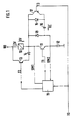
- Figure 1 shows a possible implementation of the switching device according to the invention
- Figure 2 shows a voltage-current diagram with current limitation
- Figure 3 shows a voltage-current diagram without current limitation
- the exemplary embodiments described are switching devices for fast switching of electromagnetic consumers.
- the switching devices described can be used in connection with any electromagnetic consumer, that is, they are not restricted to a specific application.
- a solenoid valve can then be used in a particularly advantageous manner for injecting fuel into the internal combustion engine.
- a solenoid valve 10 a switching transistor 11 and a measuring resistor 12 form a series connection from the battery voltage UB to ground.
- the current that flows through the solenoid valve 10 is denoted by IV, the voltage at the solenoid valve 10 by UV.
- IV the current that flows through the solenoid valve 10
- UV the voltage at the solenoid valve 10
- the drive signal T2 is located at the base of the freewheel transistor 13.
- connection point of the solenoid valve 10 and the switching transistor 11 From the connection point of the solenoid valve 10 and the switching transistor 11, the parallel connection of a control diode 15 and a control transistor 17 leads to a connection point of a control capacitance 16.
- the second connection point of this control capacitance 16 is connected to the connection point of the switching transistor 11 and the measuring resistor 12.
- the voltage applied to the control capacitance 16 is identified by UC.
- the control transistor 17 becomes at its base with the control signal T3.
- the diode 18 is also connected in parallel with the switching transistor 11.
- the switching transistor 11 itself is controlled by the control signal T1.
- the voltage at the connection point of solenoid valve 10 and switching transistor 11 is designated UM1, while the voltage at the connection point of switching transistor 11 and measuring resistor 12 is identified by UM2.
- Reference number 19 denotes a control and / or regulating device.
- This control and / or regulating device 19 receives at least the signals UM1, UM2, and a basic control signal To, and, depending on these input signals, forms at least one or more output signals, with the aid of which the transistors 11, 13 can be used directly or indirectly and 17 can be controlled.
- FIGS. 2, 3 and 4a to d in the text below show voltage-current diagrams with and without current limitation.
- the valve voltage UV and the valve current IV are plotted over time in these two figures.
- IA denotes the so-called pull-in current in both FIGS. 2 and 3, that is, the current which is sufficient for the pulling-in of the solenoid valve, that is to say for the transition of the solenoid valve from one operating state to the other.
- IH1 and IH2 are two holding currents that form the lower and upper current limit for controlling the current through the solenoid valve.
- the lower limit value that is to say the holding current IH1
- the control of the solenoid valve begins at time to. From time t1, the current IV is limited by the solenoid valve.
- the time t2 marks the so-called valve stop, that is, the complete transition of the solenoid valve from its one to its other operating state. From time t3, the solenoid valve is activated in a clocked manner, the valve current IV increases and decreases regularly.
- Time t4 marks the end of activation of the solenoid valve.
- FIGS. 4a to d show diagrams of the control signals with current limitation.
- the basic control signal To for the solenoid valve is shown in FIG. 4a, the control signal T1 for the switching transistor 11 in FIG. 4b, the control signal T2 for the freewheeling transistor 13 in FIG. 4c, and the control signal T3 for the control transistor 17 in FIG. 4d for the times to to t4 correspond to the designations of FIGS. 2 and 3.
- voltages are plotted over time in FIGS. 4a to d.
- the voltages are the voltages that are applied to the base of the respective transistors. The voltages are not drawn to scale.
- the basic control signal To is still at ground before the time to, this has the consequence that, based on the control signals T1, T2, T3 in FIGS. 4b to d, the switching transistor 11 and the freewheeling transistor 13 are blocked, while the control transistor 17 is switched on .
- the current IV through the solenoid valve 10 is before the time to equal to 0.
- the solenoid valve 10 should now change to its other operating state as quickly as possible.
- the control signal T1 and the control signal T3 is also changed at the time to such that the switching transistor 11 changes to its conductive state while the control transistor 17 is now blocking.
- valve current IV exceeds at least the value of starting current IA.
- the valve current IV is controlled from the time t1 in such a way that it maintains the value of the starting current IA or an even greater current. This is achieved in that the voltage UV at the solenoid valve is reduced on the basis of the control signal T1 according to FIG. 4b.
- no current limitation is carried out, ie the current IV is not limited to the value of the current IA.
- the current IV rises evenly and the voltage UV remains constant.
- the solenoid valve has completely changed into its other operating state.
- This can be seen in FIG. 2, for example, in that the voltage UV at the solenoid valve has a kink at this valve stop time.
- This valve stop is identified in FIG. 3 by an analog kink in the current IV through the solenoid valve.
- the switching transistor 11 is switched off in both cases, that is to say with and without current limitation, after the detection of the time t2. So now all three transistors 11, 13 and 17 are in their non-conductive state.
- the current IV through the solenoid valve 10 smaller.
- the current IV now reaches the value of the holding current IH1.
- the switching transistor 11 and the freewheeling transistor 13 are now converted into their conductive operating states. This has the consequence that the current IV through the solenoid valve 10 increases again. If the current IV then reaches the value of the holding current IH2, the switching transistor 11 is switched off again, as a result of which the current IV becomes smaller again.
- the switching transistor 11 When the switching transistor 11 is conductive, the current IV flows through the solenoid valve 10, the switching transistor 11 and the measuring resistor 12, while when the switching transistor 11 is blocked, the current IV flows from the solenoid valve 10 via the diode 14 and the freewheeling transistor 13.
- the voltage at the solenoid valve 10 is at a positive potential when the transistor 11 is conductive, while it is zero when the transistor 11 is blocked.
- the clocking between the two times t3 and t4 is effected solely by switching the switching transistor 11 back and forth.
- the free-wheeling transistor 13 is switched on during this entire period and the control transistor 17 still blocked.
- the time t4 marks the end of the actuation of the solenoid valve 10, so the solenoid valve 10 should now return to its initial operating state as quickly as possible.
- the basic control signal To is reset to ground in accordance with FIG. 4a, and in accordance with FIGS. 4b to d the switching transistor 11 and the freewheeling transistor 13 are blocked, however, the control transistor 17 is brought into its conductive operating state .
- the current IV flowed either between the elements 10, 11, 12 or 10, 14, 13 between the two times t3 and t4, but now after the time t4 these current paths through the blocked transistors 11 and 13 are no longer possible.
- the current IV through the solenoid valve 10 cannot jump and is still positive at the time t4, the current IV flows between the time t4 and the time t5 via the solenoid valve 10, the diode 15, the control capacitance 16 and the measuring resistor 12 to ground.
- the current IV becomes smaller and smaller from time t4 and is zero at time t5.
- the valve current IV thus becomes negative, as is also shown in the two FIGS. 2 and 3. This means that now, ie after time t5, the control capacitor 16 drives a current against the battery voltage UB via the control transistor 17 into the solenoid valve 10 due to its applied voltage UC.
- this negative current IV through the solenoid valve 10 reaches its maximum negative value relatively quickly, and then rises again to become zero at time t7. Since, as has been stated, the control transistor 17 is turned on at the time t4, the voltage UV at the solenoid valve 10 is switched to a large, negative value at this time t4. From time t5, however, the valve voltage UV rises again in order to change from negative to positive values again at time t6. At time t7, the voltage UV at the solenoid valve 10, like the valve current IV, finally becomes zero.
- the free-wheeling transistor 13 can also be clocked between the two times t3 and t4. It is only important here that the freewheeling transistor 13 is in its conductive operating state when the switching transistor 11 blocks. It is also possible not to switch the control transistor 17 conductive at time t4, but at a later time. However, the last possible time for switching the control transistor 17 is the time t5, that is to say the zero crossing of the current IV through the solenoid valve 10.
- the times to and t4 that is to say the basic control signal of the solenoid valve 10, can be freely specified by the user of the switching device according to the invention described.
- the time t1 can be recognized, for example, by the control and / or regulating device 19 with the aid of the measuring voltage UM2, in order then to take the appropriate measures for limiting the current of the valve current IV.
- time t2 is the valve stop time.
- the time t2 can be recognized during operation according to FIG. 2, for example, with the aid of the measurement voltage UM1 and thus due to the kink in the valve voltage UV, or during operation according to FIG.
- the time t3 is, as already mentioned, reached when after the time t2 the valve current IV has reached the value of the holding current IH1 for the first time.
- the subsequent clocking is then defined by the two holding currents IH1 and IH2.
- the switching device also has the advantage that the state of the solenoid valve is precisely defined by the two times t2 and t4. If, for example, the solenoid valve is in its closed state before the time to, it has changed to its open state exactly at the time t2 and closed again shortly after the time t4. With the help of these clearly defined operating states, it is then possible to set up a time control loop.
- the switching device according to the invention in particular in comparison with the prior art, also has the advantage that only a relatively low power loss occurs because the energy of the current quenching is fed back into the solenoid valve with the aid of the capacitance.
- the current load on the entire circuit becomes a minimum and the power loss increases only slightly.
- the magnetic saturation of the solenoid valve is limited in this case, so that the time t2 can be recognized particularly reliably.
- controllable capacitance need not be limited to a discrete electrical component, but can also be e.g. be reproduced with the help of electronic or other circuits.
Landscapes
- Engineering & Computer Science (AREA)
- Chemical & Material Sciences (AREA)
- Combustion & Propulsion (AREA)
- Mechanical Engineering (AREA)
- General Engineering & Computer Science (AREA)
- Fuel-Injection Apparatus (AREA)
- Electronic Switches (AREA)
- Magnetically Actuated Valves (AREA)
- Electrical Control Of Air Or Fuel Supplied To Internal-Combustion Engine (AREA)
Claims (12)
- Circuit de commutation pour la commutation rapide de charges électromagnétiques comportant un montage en série formé d'au moins une charge électromagnétique (10) et au moins un premier dispositif de commutation (11) avec au moins une diode en roue libre (14) pour la charge électromagnétique (10), un condensateur (16) pouvant être commandé en parallèle sur le premier dispositif de commutation (11), circuit caractérisé en ce que le chemin de charge et de décharge du condensateur (16) est commuté à l'aide d'un second dispositif de commutation (17) branché en série sur ce condensateur pour que pendant l'état de blocage du premier dispositif de commutation (11), un courant de charge et de décharge puisse traverser le condensateur (16) par l'intermédiaire de la charge (10).
- Circuit de commutation selon la revendication 1, caractérisé par une diode (15) branchée en série sur le condensateur (16).
- Circuit de commutation selon l'une des revendications 1 et 2, caractérisé en ce que la diode (15) est branchée en parallèle sur le second dispositif de commutation (17).
- Circuit de commutation selon l'une des revendications 1 à 3, caractérisé par un troisième dispositif de commutation (13) branché en série sur la diode de roue libre (14).
- Circuit de commutation selon l'une des revendications 1 à 4, caractérisé en ce qu'il est appliqué en liaison avec le dosage du carburant dans une chambre de combustion d'un moteur à combustion interne.
- Circuit de commutation selon l'une des revendications 1 à 5, caractérisé en ce que la charge électromagnétique (10) est l'électrovanne d'injection de carburant dans la chambre de combustion d'un moteur à combustion interne.
- Procédé de mise en oeuvre d'un circuit de commutation avec un montage en série formé d'au moins une charge électrique (10) et un premier dispositif de commutation (11), au moins une diode de roue libre (14) pour l'utilisateur électromagnétique (10), un condensateur (16), commutable en parallèle sur le premier dispositif de commutation (11), un second dispositif de commutation (17) en série sur le condensateur (16) ainsi qu'un troisième dispositif de commutation (13) en série sur la diode de roue libre (14), procédé caractérisé en ce qu au cours d'une première période seul le premier dispositif de commutation (11) en série sur la charge électromagnétique (10) est passant.
- Procédé selon la revendication 7, caractérisé en ce qu'au cours d'une seconde période, tous les dispositifs de commutation (11, 13, 17) sont bloqués.
- Procédé selon l'une des revendications 7, 8, caractérisé en ce que pendant une troisième période, le dispositif de commutation (11) en série sur la charge électromagnétique (10) est commandé en alternance entre son état passant et son état bloqué et inversement.
- Procédé selon l'une des revendications 7 à 9, caractérisé en ce qu'au cours d'une quatrième période, seul le dispositif de commutation (17) en série sur le condensateur (16) est passant.
- Procédé selon l'une des revendications 7 à 10, caractérisé en ce que pendant la première période, le dispositif de commutation (11) en série sur la charge électromagnétique (10) limite au moins de temps à autre le courant traversant la charge électromagnétique (10).
- Procédé selon la revendication 11, caractérisé en ce qu'à l'aide de la limitation d'intensité, on influence la saturation magnétique de la charge électromagnétique (10) et on détecte ainsi de manière particulièrement sûre la fin de la première période.
Applications Claiming Priority (2)
| Application Number | Priority Date | Filing Date | Title |
|---|---|---|---|
| DE19843442764 DE3442764A1 (de) | 1984-11-23 | 1984-11-23 | Schalteinrichtung zum schnellen schalten elektromagnetischer verbraucher |
| DE3442764 | 1984-11-23 |
Publications (3)
| Publication Number | Publication Date |
|---|---|
| EP0182101A2 EP0182101A2 (fr) | 1986-05-28 |
| EP0182101A3 EP0182101A3 (en) | 1988-09-21 |
| EP0182101B1 true EP0182101B1 (fr) | 1991-03-13 |
Family
ID=6250993
Family Applications (1)
| Application Number | Title | Priority Date | Filing Date |
|---|---|---|---|
| EP19850113155 Expired - Lifetime EP0182101B1 (fr) | 1984-11-23 | 1985-10-17 | Dispositif commutateur pour commuter rapidement des charges électromagnétiques |
Country Status (4)
| Country | Link |
|---|---|
| US (1) | US4639822A (fr) |
| EP (1) | EP0182101B1 (fr) |
| JP (1) | JPH0758898B2 (fr) |
| DE (2) | DE3442764A1 (fr) |
Families Citing this family (12)
| Publication number | Priority date | Publication date | Assignee | Title |
|---|---|---|---|---|
| US4862866A (en) * | 1987-08-25 | 1989-09-05 | Marelli Autronica S.P.A. | Circuit for the piloting of inductive loads, particularly for operating the electro-injectors of a diesel-cycle internal combustion engine |
| DE4018320C2 (de) * | 1990-06-08 | 2002-06-27 | Bosch Gmbh Robert | Ansteuerschaltung für einen elektromagnetischen Verbraucher |
| DE4130711A1 (de) * | 1991-09-14 | 1993-03-18 | Kloeckner Humboldt Deutz Ag | Steuerung elektromagnetischer ventile |
| DE4140586C2 (de) * | 1991-12-10 | 1995-12-21 | Clark Equipment Co N D Ges D S | Verfahren und Steuereinrichtung zur Steuerung des Stroms durch eine Magnetspule |
| US5796223A (en) * | 1996-07-02 | 1998-08-18 | Zexel Corporation | Method and apparatus for high-speed driving of electromagnetic load |
| US5930104A (en) * | 1998-03-06 | 1999-07-27 | International Controls And Measurement Corp. | PWM relay actuator circuit |
| DE19815628C1 (de) * | 1998-04-07 | 1999-09-23 | Siemens Ag | Steuereinrichtung für ein Kraftstoff-Einspritzsystem |
| JP2003086422A (ja) * | 2001-09-12 | 2003-03-20 | Bosch Automotive Systems Corp | 電磁弁駆動装置 |
| DE102004062020A1 (de) * | 2004-12-23 | 2006-07-13 | Robert Bosch Gmbh | Verfahren zum Betrieb einer Brennkraftmaschine |
| DE102009044953B4 (de) * | 2009-09-24 | 2019-12-05 | Robert Bosch Gmbh | Verfahren zum Ansteuern eines elektromagnetischen Verbrauchers sowie entsprechende Schaltung |
| DE102013213028B3 (de) | 2013-07-03 | 2014-08-21 | Continental Automotive Gmbh | Schaltungsanordnung zum Schalten externer Lasten mit Schutzschaltung |
| US10666146B2 (en) | 2018-03-05 | 2020-05-26 | Texas Instruments Incorporated | Bidirectional inverting buck-boost converter converting dissipation current into recycling current |
Citations (1)
| Publication number | Priority date | Publication date | Assignee | Title |
|---|---|---|---|---|
| EP0074536A2 (fr) * | 1981-09-10 | 1983-03-23 | Robert Bosch Gmbh | Dispositif de commutation électrique pour appareil de commande d'un véhicule à moteur |
Family Cites Families (12)
| Publication number | Priority date | Publication date | Assignee | Title |
|---|---|---|---|---|
| US4225898A (en) * | 1978-02-27 | 1980-09-30 | The Bendix Corporation | Inductive driver circuit effecting slow and fast current decay |
| US4234903A (en) * | 1978-02-27 | 1980-11-18 | The Bendix Corporation | Inductive load driver circuit effecting slow hold current delay and fast turn off current decay |
| EP0028090B1 (fr) * | 1979-10-25 | 1985-02-13 | LUCAS INDUSTRIES public limited company | Circuit de commande pour un électro-aimant |
| JPS5675956A (en) * | 1979-11-27 | 1981-06-23 | Nippon Denso Co Ltd | Injector driving circuit |
| EP0047614B1 (fr) * | 1980-09-06 | 1985-08-21 | LUCAS INDUSTRIES public limited company | Circuit pour commander un électro-aimant |
| JPS5749059A (en) * | 1980-09-08 | 1982-03-20 | Toshiba Corp | Driving circuit of injector |
| JPS5851233A (ja) * | 1981-09-21 | 1983-03-25 | Hitachi Ltd | 燃料噴射弁駆動回路 |
| JPS5858866A (ja) * | 1981-10-05 | 1983-04-07 | Toshiba Corp | スイッチング装置 |
| DE3139987A1 (de) * | 1981-10-08 | 1983-04-28 | Robert Bosch Gmbh, 7000 Stuttgart | Steuereinrichtung fuer einen elektromagnetischen verbraucher in einem kraftfahrzeug, insbesondere ein magnetventil oder ein stellmagnet |
| JPS58121521A (ja) * | 1982-01-13 | 1983-07-19 | オムロン株式会社 | 電子式タイマ装置 |
| FR2538942B1 (fr) * | 1982-12-29 | 1989-05-05 | Renault | Dispositif de commande d'organe(s) electromagnetique(s) a actionnement rapide, tel(s) qu'electrovanne(s) ou injecteur(s) |
| US4511945A (en) * | 1983-12-27 | 1985-04-16 | Ford Motor Company | Solenoid switching driver with fast current decay from initial peak current |
-
1984
- 1984-11-23 DE DE19843442764 patent/DE3442764A1/de not_active Ceased
-
1985
- 1985-08-28 US US06/770,646 patent/US4639822A/en not_active Expired - Fee Related
- 1985-10-17 DE DE8585113155T patent/DE3582115D1/de not_active Expired - Lifetime
- 1985-10-17 EP EP19850113155 patent/EP0182101B1/fr not_active Expired - Lifetime
- 1985-10-24 JP JP60236546A patent/JPH0758898B2/ja not_active Expired - Lifetime
Patent Citations (1)
| Publication number | Priority date | Publication date | Assignee | Title |
|---|---|---|---|---|
| EP0074536A2 (fr) * | 1981-09-10 | 1983-03-23 | Robert Bosch Gmbh | Dispositif de commutation électrique pour appareil de commande d'un véhicule à moteur |
Also Published As
| Publication number | Publication date |
|---|---|
| DE3442764A1 (de) | 1986-05-28 |
| JPS61131614A (ja) | 1986-06-19 |
| JPH0758898B2 (ja) | 1995-06-21 |
| EP0182101A2 (fr) | 1986-05-28 |
| EP0182101A3 (en) | 1988-09-21 |
| US4639822A (en) | 1987-01-27 |
| DE3582115D1 (de) | 1991-04-18 |
Similar Documents
| Publication | Publication Date | Title |
|---|---|---|
| DE69533962T2 (de) | Gleichstromwandler und denselben verwendende steuereinrichtung für induktive last | |
| EP0074536B1 (fr) | Dispositif de commutation électrique pour appareil de commande d'un véhicule à moteur | |
| EP1527470B1 (fr) | Ensemble de commande pour entrainement electromagnetique | |
| EP0491731B1 (fr) | Element de reseau combinatoire | |
| EP0182101A2 (fr) | Dispositif commutateur pour commuter rapidement des charges électromagnétiques | |
| DE2932859A1 (de) | Einrichtung zum steuern des stromes durch einen induktiven verbraucher, insbesondere ein magnetventil im kraftstoffzumesssystem einer brennkraftmaschine | |
| DE3111757A1 (de) | Steuerschaltung fuer einen vollsteuergate-thyristor | |
| DE3712784A1 (de) | Schaltungsanordnung zur begrenzung der einschaltstromspitzen bei einem schalttransistor | |
| DE3878489T2 (de) | Schaltsystem zum aufladen/entladen eines kondensators. | |
| DE3327393A1 (de) | Steuereinrichtung zum schnelleren schalten eines elektromagnetischen verbrauchers, insbesondere in verbindung mit brennkraftmaschinen | |
| DE2461583C2 (de) | Schaltung zur Reduzierung der Einschaltverluste eines Leistungstransistors | |
| EP0195267A2 (fr) | Circuit de commande du courant dans un consommateur électrique, en particulier électromagnétique | |
| DE3634990A1 (de) | Verlustarmes spannungsbegrenzungsnetzwerk fuer sperr- oder flusswandler | |
| DE69413206T2 (de) | Kraftstoffeinspritzsteuervorrichtung für eine brennkraftmaschine | |
| DE60102179T2 (de) | Resonanzschaltnetzteil | |
| DE2706436C2 (fr) | ||
| EP0854281B1 (fr) | Dispositif de pilotage d'au moins un consommateur électromagnetique | |
| DE19701958C2 (de) | Mit höherer Frequenz betriebene Leistungsstufe für eine Sitzheizungsschaltung | |
| DE3212942C2 (fr) | ||
| EP0203419A1 (fr) | Alimentation de puissance à découpage sur le circuit primaire | |
| DE69009006T2 (de) | Schaltung zur impulsförmigen Versorgung induktiver Lasten mit einer Spannungsbegrenzung. | |
| DE2524680C3 (de) | Transistorbestückter Multivibrator | |
| DE1102812B (de) | Zeitsteuerschaltung | |
| DE2531510A1 (de) | Schaltung zur ueberwachung einer spannungsquelle | |
| AT217112B (de) | Schutzschaltung für Transistoren |
Legal Events
| Date | Code | Title | Description |
|---|---|---|---|
| PUAI | Public reference made under article 153(3) epc to a published international application that has entered the european phase |
Free format text: ORIGINAL CODE: 0009012 |
|
| AK | Designated contracting states |
Kind code of ref document: A2 Designated state(s): DE FR GB |
|
| PUAL | Search report despatched |
Free format text: ORIGINAL CODE: 0009013 |
|
| AK | Designated contracting states |
Kind code of ref document: A3 Designated state(s): DE FR GB |
|
| 17P | Request for examination filed |
Effective date: 19890216 |
|
| 17Q | First examination report despatched |
Effective date: 19891102 |
|
| GRAA | (expected) grant |
Free format text: ORIGINAL CODE: 0009210 |
|
| AK | Designated contracting states |
Kind code of ref document: B1 Designated state(s): DE FR GB |
|
| ET | Fr: translation filed | ||
| GBT | Gb: translation of ep patent filed (gb section 77(6)(a)/1977) | ||
| REF | Corresponds to: |
Ref document number: 3582115 Country of ref document: DE Date of ref document: 19910418 |
|
| PLBE | No opposition filed within time limit |
Free format text: ORIGINAL CODE: 0009261 |
|
| STAA | Information on the status of an ep patent application or granted ep patent |
Free format text: STATUS: NO OPPOSITION FILED WITHIN TIME LIMIT |
|
| RAP4 | Party data changed (patent owner data changed or rights of a patent transferred) |
Owner name: ROBERT BOSCH GMBH |
|
| 26N | No opposition filed | ||
| PGFP | Annual fee paid to national office [announced via postgrant information from national office to epo] |
Ref country code: GB Payment date: 19951004 Year of fee payment: 11 |
|
| PGFP | Annual fee paid to national office [announced via postgrant information from national office to epo] |
Ref country code: FR Payment date: 19951018 Year of fee payment: 11 |
|
| PG25 | Lapsed in a contracting state [announced via postgrant information from national office to epo] |
Ref country code: GB Effective date: 19961017 |
|
| PGFP | Annual fee paid to national office [announced via postgrant information from national office to epo] |
Ref country code: DE Payment date: 19961213 Year of fee payment: 12 |
|
| GBPC | Gb: european patent ceased through non-payment of renewal fee |
Effective date: 19961017 |
|
| PG25 | Lapsed in a contracting state [announced via postgrant information from national office to epo] |
Ref country code: FR Effective date: 19970630 |
|
| REG | Reference to a national code |
Ref country code: FR Ref legal event code: ST |
|
| PG25 | Lapsed in a contracting state [announced via postgrant information from national office to epo] |
Ref country code: DE Free format text: LAPSE BECAUSE OF NON-PAYMENT OF DUE FEES Effective date: 19980701 |