EP0182254B1 - Punktmatrix-Leuchtanzeige - Google Patents
Punktmatrix-Leuchtanzeige Download PDFInfo
- Publication number
- EP0182254B1 EP0182254B1 EP85114372A EP85114372A EP0182254B1 EP 0182254 B1 EP0182254 B1 EP 0182254B1 EP 85114372 A EP85114372 A EP 85114372A EP 85114372 A EP85114372 A EP 85114372A EP 0182254 B1 EP0182254 B1 EP 0182254B1
- Authority
- EP
- European Patent Office
- Prior art keywords
- holes
- dot matrix
- luminous
- luminous display
- electrodes
- Prior art date
- Legal status (The legal status is an assumption and is not a legal conclusion. Google has not performed a legal analysis and makes no representation as to the accuracy of the status listed.)
- Expired - Lifetime
Links
Images



Classifications
-
- H—ELECTRICITY
- H10—SEMICONDUCTOR DEVICES; ELECTRIC SOLID-STATE DEVICES NOT OTHERWISE PROVIDED FOR
- H10W—GENERIC PACKAGES, INTERCONNECTIONS, CONNECTORS OR OTHER CONSTRUCTIONAL DETAILS OF DEVICES COVERED BY CLASS H10
- H10W90/00—Package configurations
Definitions
- the present invention relates to a dot-matrix luminous display comprising a dot matrix display board having an insulating plate; first and second sets of electrodes provided on respective opposite surfaces of said insulating plate; a plurality of light emitting-elements and a plurality of through-holes through which said light emitting-elements are electrically coupled between said electrodes of said first and second sets, respectively; and a member provided over said one surface of said dot matrix display board, said member having a plurality of through-holes formed therein at locations corresponding to locations of said light-emitting elements.
- Luminous displays of this type are designed to display desired characters, symbols or patterns in the form of a dot pattern by supplying power to and lighting selected luminous elements arranged in a matrix.
- the basic structure of such a matrix display includes upper and lower electrodes arranged in a three-dimensional matrix with an insulating layer sandwiched therebetween, and semiconductor chips disposed at intersections between the upper and lower electrodes.
- a matrix luminous display board (hereinafter referred to as simply a "matrix board” or “display board”) 1 with the upper and lower electrodes 100 and 101 arranged in a three-dimensional matrix.
- matrix board or “display board”
- through-holes 104 in portions where the upper and lower electrodes 100 and 101 intersect.
- a semiconductor chip 105 forming a single luminous element, is supplied in each through-hole 104, and, as a final process, the entire surface of the matrix board 1, including the through-holes 104 through which are exposed the semiconductor chips 105, is coated with a translucent thermosetting resin to provide thereby a continuous protective film 107.
- bonding wires 106 are used to connect the semiconductor chips 105 to the upper electrodes 100, whereas solder or silver paste 108 is used to provide conductive connection between the bottoms of the semiconductor chips 105 and the lower electrodes 101.
- the spacing between outer edges of adjacent through-holes 104 is about 8.0 mm, the diameter of each through-hole 104 is about 6.5 mm, and the length of a side of the display board 1, is about 64 mm.
- strains such as strains there may be produced strain, camber, peeling and cracks (hereinafter collectively referred to as "flaws such as strains") at the joints of the matrix board 1 and the protective film 107 because of the difference therebetween in the coefficient of thermal expansion. These flaws such as strains result in defective products.
- the flaws such as strains become more pronounced as the size of the matrix board 1 is increased. Even finished products are not free from such strains caused by, for instance, the temperature difference between summer and winter or heat generated when power is supplied to the luminous elements.
- the present invention is intended to solve the aforementioned problems.
- the inventive dot matrix luminous display is characterized in that said member is elastic, consists of silicon rubber, neoprene rubber, flexible epoxy resin or flexible acrylic resin, and is flexible relative to that dot matrix display board and that said through-holes of said elastic member being filled with a thermosetting resin, wherein contraction of said thermosetting resin resulting from hardening of said thermosetting resin is absorbed by said rubber member.
- Fig. 3 is a schematic exploded view illustrating a matrix luminous display according to the present invention.
- Fig. 4 is an enlarged view of a portion A indicated in Fig. 3.
- Fig. 5 is a vertical sectional view illustrating principal portions with the flexible plate joined.
- the luminous display according to the present invention includes the flexible plate 2 with through-holes 200 provided therein joined to the surface of the matrix board 1.
- the flexible plate 2 is prepared from a flexible material.
- an etching process is applied to the top and bottom faces of a glass epoxy laminated plate, to the top and bottom faces of which have been adhered copper foil, to remove undesired portions of the copper foil so as to provide upper electrodes 100 and lower electrodes 101 arranged in a three-dimensional matrix, including cross conductive portions 111.
- the cross conductive portions 111 are provided inside respective insulating portions 110, formed in a part of the upper electrode 100 above the lower electrodes 101, and are coupled to the lower electrodes 101 through respective through-holes 109 provided in the center of the insulating portions 110.
- the surface of each cross conductive portion 111 is plated, and a portion surrounding the cross conductive portion 111 is plated to form a conductive portion 113.
- a print circuit board having a glass epoxy laminated plate as a substrate is described as the material of the matrix board 1 in this embodiment, the material is not particularly restricted and, for instance, a paper phenol laminated plate lined with copper and a composite plate as shown in Fig. 1 can be used.
- the lower surfaces of semiconductor chips 105, used as the luminous elements are fixed with silver paste (not shown) to the conductive portion 113, whereas the upper surfaces of the semiconductor chips 105 are bonded by wires 106 to a plated portion 112 of the upper electrode 100.
- Well known types of pn junction light-emitting diodes such as those of the gallium phosphorus (GaP) type, gallium arsenic (GaAs) type, gallium aluminum arsenic (GaAlAs) type etc., are preferably employed for the semiconductor chips 105 constituting the luminous elements used in the present invention, but other types may be used as well.
- GaP gallium phosphorus
- GaAs gallium arsenic
- GaAlAs gallium aluminum arsenic
- the flexible plate 2 prepared from a flexible material is provided with through-holes 200 at location corresponding to the semiconductor chips 105 arranged on the matrix board 1.
- the material used to prepare the flexible plate 2 is preferably one of silicon rubber, neoprene rubber, flexible epoxy resin, or flexible acrylic resin, and most preferably a heat resistant material.
- each through-hole 200 It is also preferred to apply white or silver paint to the inside surface of each through-hole 200 to improve the luminous flux radiated from the luminous element 105 and to obtain clearer light emission by preventing light from leaking to neighboring portions.
- the flexible plate 2 itself of a white material having an excellent light reflection efficiency. Accordingly, the finished dot matrix luminous display thus constructed is obtained by joining the flexible plate 2 to the surface of the matrix board 1, pouring translucent thermosetting resin into each through-hole 200 in the flexible plate 2, then thermosetting the resin to form a protective film 107 (see Fig. 5).
- positive and negative driver terminals are respectively connected to the upper electrode 100 and the lower electrode 101, and a dynamic drive circuit is used to display desired characters, symbols and patterns in the form of a dot patterns by selectively supplying power to and lighting the luminous elements 105 by the selection of combinations of electrodes, as is well known.
- Fig. 6 is a perspective exploded view illustrating an application of the present invention to a 8 x 8 dot matrix luminous display, which includes a display board 1, luminous portions 7 formed by semiconductor chips such as light-emitting diodes, and an flexible plate 2 provided with through-holes 200 corresponding in location to the luminous portions 7.
- the display board 1 is provided with an electrode pattern (represented by X and Y electrodes in this case), formed by etching the top and bottom faces of a laminated plate lined with copper, and luminous portions 7 including semiconductor chips 7a, such as light-emitting diodes, fixed thereto.
- the luminous portions 7 are arranged in a matrix.
- Table 1 shows a concrete example of a 8 x 8 dot matrix luminous display.
- Side length of display board 64 mm Diameter of through holes: 6.5 mm Spacing between through holes: 8.0 mm Thickness of matrix board: 1.6 mm Thickness of flexible plate: 1.5 to 2.0 mm
- the dot matrix luminous display plate thus constructed, because no through-holes are present in the display board in the areas of the luminous portions, the above described process of filling these holes is unnecessary when the through-holes in the flexible plate are filled with thermosetting resin. Thus, the manufacturing efficiency of the display is significantly improved.
- the flexible plate has through-holes in locations corresponding to the luminous portions and not the through-holes in the display board, it is only necessary to fill the through-holes in the locations corresponding to the luminous portions with thermosetting resin and to harden the resin. Accordingly, since only those through-holes must be filled with the thermosetting resin, there is little likelihood of leakage from the backside of the display board.
- Fig. 7 is a diagram illustrating the electrode pattern arranged on the surface of the display board 1.
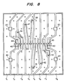
- Fig. 8 is a diagram illustrating the rear side of the electrode pattern.
- through-holes 40 including through-holes 44 and 45, in a horizontal row where connector terminals are installed.
- the connector terminals on the electrode X and Y sides are alternately arranged.
- the connector terminals on the electrode X side are respectively connected to the electrodes X (X1 to X8) via through-holes 41 to 48, whereas those on the electrode Y side are respectively connected to vertically extending electrodes 21 via through-holes 4 corresponding to the luminous portions 7.
- Figs. 6 through 11 the portions designated by alternate long and short dashed lines are the luminous portions 7 where the semiconductor chips 7a are installed.
- the luminous portions 7 are conductively plated and supplied with the semiconductor chips 7a by means of silver paste, the semiconductor chips 7a being wire-bonded to the vertically extending electrodes 21.
- Fig. 9 is an enlarged view of a luminous portion 7 in Fig. 6.
- the flexible plate 2 is joined to the display board 1 in such a manner as to match the through-holes 200 thereof to the luminous portions 7 on the display board 1.
- Each of the through-holes 200 of the flexible plate 2 is filled with thermosetting resin (not shown) to complete the dot matrix luminous display.
- fitting holes 20 in Figs. 6 through 8 used to attach the display board 1 to a matrix drive circuit board(not shown).
- a connector (not shown) is fitted to the connected terminal, and then connected to a matrix drive circuit (not shown).
- the luminous portions 7 are then selectively supplied with power by driving selected combinations of the electrodes X and Y in such a manner that dot patterns in the form of desired characters or symbols are displayed.
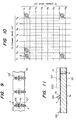
- Fig. 10 shows an electrical equivalent circuit of the display board 1 with two semiconductor chips 7a (light-emitting diodes) connected to each luminous portion 7 in parallel.
- Fig. 11 illustrates the relationship of the display board 1 to the through-hole 200 of the flexible plate 2 in a vertical sectional structural diagram.
- no through-holes 4 are provided for the display board 1 in areas corresponding to the through-holes 200 of the flexible plate 2, and it will thus be readily understood that the through-holes 4 are formed in areas other than those where the through-holes 200 are made.
- Fig. 12 is a diagram illustrating an electrode pattern of another example of the display board 1, wherein the through-hole 4 is made so that the semiconductor chips 7a bonded on the electrode X (X n ) are electrically wire-bonded to the electrode pattern 101' extending to the luminous portion 7, and consequently the through-hole 4 is seen to be provided in an area other than that where the through-hole 200 of the flexible plate 2 is made.
- the present invention is characterized in that the through-holes 4 and 40 to 48 are provided in areas other than those corresponding to the through-holes 200 of the flexible plate 2.
- any structure of the flexible plate 2 is acceptable, but it is preferred, as in the case of the first-described embodiment, to prevent the formation of strains and cracks by employing a material whose coefficient of thermal expansion conforms to that of the display board 1, or one prepared from a flexible resin, if the flexible plate 2 is selected in terms of its structural properties.
- the present invention is not limited to dot matrix luminous displays as described above and, as proposed in Japanese Patent No. 59-27606, is applicable to a plurality of display boards provided with luminous portions forming a body of segments.
- Fig. 13 illustrates such an embodiment.
- Fig. 13 shows an arrangement of a body of segments 1' provided with luminous portions 7 and an insulating board 11 carrying an electrode pattern 11a, wherein the electrode pattern portion 24 of the body of segments 1' is connected to the electrode pattern 11a via through-holes 105 provided in areas other than those (shown by alternating long and two dashed lines) corresponding to the through-holes 200 of the flexible plate 2.
- the flexible plate 2 has been omitted in Fig. 13.
Landscapes
- Devices For Indicating Variable Information By Combining Individual Elements (AREA)
- Led Device Packages (AREA)
Claims (10)
- Eine Punktmatrix-Leuchtanzeige mit:
einer Punktmatrix-Anzeigetafel (1), die eine Isolierplatte (110) aufweist;
ersten und zweiten Sätzen von Elektroden (100, 101), die an entsprechend gegenüberliegend angeordneten Oberflächen der Isolierplatte (110) vorgesehen sind;
einer Mehrzahl von lichtemittierenden Elementen (105; 7) und einer Mehrzahl von Durchgangslöchern (109), durch welche die lichtemittierenden Elemente (105; 7) zwischen den Elektroden (100, 101) der ersten bzw. zweiten Sätze elektrisch gekoppelt sind;
und einem Teil (2), das über der einen Oberfläche der Punktmatrix-Anzeigetafel (1) vorgesehen ist, wobei das Teil (2) mehrere darin ausgebildete Durchgangslöcher (200) an Stellen aufweist, die den Stellen der lichtemittierenden Elemente (105; 7) entsprechen,
dadurch gekennzeichnet,
daß das Teil (2) elastisch ist, aus Silikon-Kautschuk, Neopren-Kautschuk, elastischem Epoxyharz oder elastischem Acrylharz besteht und relativ zu der Punktmatrix-Anzeigetafel (1) flexibel bzw. verbiegbar ist und daß die Durchgangslöcher (200) des elastischen Teils (2) mit einem wärmehärtenden Harz (107) gefüllt sind, wobei die aus der Härtung des wärmehärtenden Harzes (107) resultierende Kontraktion des wärmehärtenden Harzes (107) von dem elastischen Teil (2) absorbiert wird. - Punktmatrix-Anzeigetafel nach Anspruch 1, dadurch gekennzeichnet, daß die Durchgangslöcher (200) in dem elastischen Teil (2) darin an Stellen ausgebildet sind, die Stellen der lichtemittierenden Elemente (105) entsprechen.
- Leuchtanzeige nach Anspruch 1, dadurch gekennzeichnet, daß die Durchgangslöcher (4) in der Punktmatrix-Anzeigetafel (1) und die Durchgangslöcher (200) in dem elastischen Teil (2) zueinander versetzt sind.
- Leuchtanzeige nach Anspruch 1 oder 2, dadurch gekennzeichnet, daß die Punktmatrix-Anzeigetafel umfaßt:
mehrere in der Isolierplatte (1) ausgebildete Durchgangslöcher (109); wobei die Elektroden (100, 101) der ersten und zweiten Sätze sich an den Durchgangslöchern (109) in der Isolierplatte (110) schneiden; mehrere lichtemittierende Elemente (105), die an der Isolierplatte (1) vorgesehen sind, wobei wenigstens eines der lichtemittierenden Elemente (105) an jeder Schnittstelle der Elektroden (100, 101) der ersten und zweiten Sätze vorgesehen ist und jedes der lichtemittierenden Elemente (105) elektrisch mit den Schneidenden der Elektroden (100, 101) der ersten und zweiten Sätze gekoppelt ist. - Leuchtanzeige nach Anspruch 1 oder 3, dadurch gekennzeichnet, daß die Matrix-Anzeigetafel umfaßt:
eine Isolierplatte mit einer Mehrzahl an darin ausgebildeten Durchgangslöchern; und eine Mehrzahl von an der ersten Oberfläche der Isolierplatte vorgesehenen lichtemittierenden Elemente (7); wobei die Durchgangslöcher (4; 105) derart angepaßt sind, daß sie es einem der Sätze von ersten und zweiten Elektroden (100, 101) gestatten, durch sie hindurchzutreten um elektrisch mit den lichtemittierenden Elementen (7) auf der ersten Oberfläche der Isolierplatte elektrisch zu kontaktieren, wo die lichtemittierenden Elemente (7) und der andere, der Sätze von ersten und zweiten Elektroden vorgesehen ist. - Leuchtanzeige nach Anspruch 1 bis 5, dadurch gekennzeichnet, daß das elastische Teil (2) aus einem hitzeresistenten Material besteht.
- Leuchtanzeige nach Anspruch 1 bis 6, dadurch gekennzeichnet, daß die Durchgangslöcher (200) in dem elastischen Teil (2) mit einem lichtdurchlässigen Harz gefüllt sind.
- Leuchtanzeige nach Anspruch 1 bis 7, dadurch gekennzeichnet, daß die Isolierplatte (109; 11) eine glasepoxydlaminierte Platte ist.
- Leuchtanzeige nach Anspruch 1 bis 7, dadurch gekennzeichnet, daß die Isolierplatte (109; 11) eine papierphenollaminierte Platte ist.
- Leuchtanzeige nach Anspruch 1 bis 9, dadurch gekennzeichnet, daß die inneren Wände der Durchgangslöcher (200) in der elastischen Platte (2) von reflektierender Farbe sind.
Applications Claiming Priority (4)
| Application Number | Priority Date | Filing Date | Title |
|---|---|---|---|
| JP171487/84U | 1984-11-12 | ||
| JP1984171487U JPH064379Y2 (ja) | 1984-11-12 | 1984-11-12 | ドットマトリクス発光表示体 |
| JP1985051480U JPH0241650Y2 (de) | 1985-04-05 | 1985-04-05 | |
| JP51480/85U | 1985-04-05 |
Publications (3)
| Publication Number | Publication Date |
|---|---|
| EP0182254A2 EP0182254A2 (de) | 1986-05-28 |
| EP0182254A3 EP0182254A3 (en) | 1989-07-26 |
| EP0182254B1 true EP0182254B1 (de) | 1994-03-09 |
Family
ID=26392022
Family Applications (1)
| Application Number | Title | Priority Date | Filing Date |
|---|---|---|---|
| EP85114372A Expired - Lifetime EP0182254B1 (de) | 1984-11-12 | 1985-11-12 | Punktmatrix-Leuchtanzeige |
Country Status (4)
| Country | Link |
|---|---|
| US (1) | US4713579A (de) |
| EP (1) | EP0182254B1 (de) |
| DE (1) | DE3587772T2 (de) |
| HK (1) | HK47195A (de) |
Families Citing this family (37)
| Publication number | Priority date | Publication date | Assignee | Title |
|---|---|---|---|---|
| EP0206176B1 (de) * | 1985-06-28 | 1992-01-02 | Takiron Co. Ltd. | Matrix aus optischen Leitern für eine Punktmatrix-Leuchtanzeige |
| US5122733A (en) | 1986-01-15 | 1992-06-16 | Karel Havel | Variable color digital multimeter |
| US5561365A (en) | 1986-07-07 | 1996-10-01 | Karel Havel | Digital color display system |
| US4843280A (en) * | 1988-01-15 | 1989-06-27 | Siemens Corporate Research & Support, Inc. | A modular surface mount component for an electrical device or led's |
| US4890383A (en) * | 1988-01-15 | 1990-01-02 | Simens Corporate Research & Support, Inc. | Method for producing displays and modular components |
| US5126620A (en) * | 1988-12-19 | 1992-06-30 | Mitsubishi Denki Kabushiki Kaisha | Display element |
| US5162696A (en) * | 1990-11-07 | 1992-11-10 | Goodrich Frederick S | Flexible incasements for LED display panels |
| DE4242842C2 (de) * | 1992-02-14 | 1999-11-04 | Sharp Kk | Lichtemittierendes Bauelement zur Oberflächenmontage und Verfahren zu dessen Herstellung |
| JP2782699B2 (ja) * | 1992-03-16 | 1998-08-06 | ローム株式会社 | 光源ユニット |
| DE4335323A1 (de) * | 1993-10-18 | 1995-04-20 | Basf Lacke & Farben | Lösungen von polyimidbildenden Substanzen und deren Verwendung |
| US5644327A (en) * | 1995-06-07 | 1997-07-01 | David Sarnoff Research Center, Inc. | Tessellated electroluminescent display having a multilayer ceramic substrate |
| US6897855B1 (en) | 1998-02-17 | 2005-05-24 | Sarnoff Corporation | Tiled electronic display structure |
| US5986391A (en) * | 1998-03-09 | 1999-11-16 | Feldman Technology Corporation | Transparent electrodes |
| DE19818227A1 (de) * | 1998-04-24 | 1999-10-28 | Helmuth Klatt | Ortsveränderlicher Informationsträger |
| US6498592B1 (en) | 1999-02-16 | 2002-12-24 | Sarnoff Corp. | Display tile structure using organic light emitting materials |
| JP3553405B2 (ja) * | 1999-03-03 | 2004-08-11 | ローム株式会社 | チップ型電子部品 |
| US6414662B1 (en) | 1999-10-12 | 2002-07-02 | Texas Digital Systems, Inc. | Variable color complementary display device using anti-parallel light emitting diodes |
| GB2366900B (en) * | 2000-09-13 | 2004-12-29 | Box Consultants Ltd | A display element |
| US6743069B2 (en) * | 2001-07-12 | 2004-06-01 | Intel Corporation | Facilitating the spread of encapsulant between surfaces of electronic devices |
| US7048423B2 (en) * | 2001-09-28 | 2006-05-23 | Visteon Global Technologies, Inc. | Integrated light and accessory assembly |
| US20030063465A1 (en) * | 2001-09-28 | 2003-04-03 | Mcmillan Richard K. | Etched metal light reflector for vehicle feature illumination |
| FR2854480A1 (fr) * | 2003-04-29 | 2004-11-05 | France Telecom | Afficheur souple |
| DE10351934B4 (de) * | 2003-11-07 | 2017-07-13 | Tridonic Jennersdorf Gmbh | Leuchtdioden-Anordnung mit wärmeabführender Platine |
| ES2262398B1 (es) * | 2004-07-09 | 2008-02-16 | Odeco Electronica, S.A. | Pantalla luminosa de señalizacion. |
| US20060023446A1 (en) * | 2004-08-02 | 2006-02-02 | Eric Racoosin | Solar lighting system for a flag |
| US20060055320A1 (en) * | 2004-09-15 | 2006-03-16 | Taiwan Oasis Technology Co., Ltd. | LED panel LED display panel glue filling gateway |
| GB2424507B (en) * | 2005-03-22 | 2007-02-21 | Smartslab Ltd | Modular display system |
| USD566665S1 (en) * | 2007-04-18 | 2008-04-15 | Edison Opto Corporation | Matrix type light emitting diode assembly |
| USD575245S1 (en) * | 2007-04-24 | 2008-08-19 | Edison Opto Corporation | Matrix type light emitting diode assembly |
| FR2923318B1 (fr) * | 2007-11-02 | 2012-12-28 | Boulenger | Panneau d'affichage optique. |
| EP2175436A1 (de) | 2008-10-08 | 2010-04-14 | Richard Peter James Barton | Punktmatrix- und segmentierte Anzeigen mit gleichmäßiger Beleuchtung |
| USD611436S1 (en) * | 2009-08-16 | 2010-03-09 | Edison Opto Corporation | Planar illuminating LED module |
| CN101996984B (zh) * | 2009-08-21 | 2012-07-04 | 柏友照明科技股份有限公司 | 成形填充式凸透镜的发光二极管封装结构及其制作方法 |
| TWI354365B (en) * | 2009-08-26 | 2011-12-11 | Quasioptical led package structure for increasing | |
| CN102024804B (zh) * | 2009-09-11 | 2012-05-23 | 柏友照明科技股份有限公司 | 能够提高演色性及亮度的混光式发光二极管封装结构 |
| CN102157509B (zh) * | 2010-02-12 | 2012-11-28 | 柏友照明科技股份有限公司 | 能够提高演色性的混光式发光二极管封装结构 |
| ES2809563T3 (es) * | 2016-07-11 | 2021-03-04 | Screen Experts Gmbh | Módulo con una pluralidad de LED y tarjeta de video |
Family Cites Families (9)
| Publication number | Priority date | Publication date | Assignee | Title |
|---|---|---|---|---|
| US3590252A (en) * | 1967-11-21 | 1971-06-29 | Westinghouse Canada Ltd | Light-sensitive switching display device |
| US3780357A (en) * | 1973-02-16 | 1973-12-18 | Hewlett Packard Co | Electroluminescent semiconductor display apparatus and method of fabricating the same |
| GB1522145A (en) * | 1974-11-06 | 1978-08-23 | Marconi Co Ltd | Light emissive diode displays |
| US4000437A (en) * | 1975-12-17 | 1976-12-28 | Integrated Display Systems Incorporated | Electric display device |
| JPS5583196A (en) * | 1978-12-20 | 1980-06-23 | Nippon Telegraph & Telephone | Method of sealing thin film electroluminescent element |
| US4241277A (en) * | 1979-03-01 | 1980-12-23 | Amp Incorporated | LED Display panel having bus conductors on flexible support |
| JPS575083A (en) * | 1980-06-13 | 1982-01-11 | Tokyo Shibaura Electric Co | Display unit |
| DD200295A1 (de) * | 1981-08-12 | 1983-04-06 | Guenter Claus | Led-anzeige mit hohem informationsgehalt |
| US4603496A (en) * | 1985-02-04 | 1986-08-05 | Adaptive Micro Systems, Inc. | Electronic display with lens matrix |
-
1985
- 1985-11-12 EP EP85114372A patent/EP0182254B1/de not_active Expired - Lifetime
- 1985-11-12 US US06/796,829 patent/US4713579A/en not_active Expired - Lifetime
- 1985-11-12 DE DE3587772T patent/DE3587772T2/de not_active Expired - Fee Related
-
1995
- 1995-03-30 HK HK47195A patent/HK47195A/en not_active IP Right Cessation
Also Published As
| Publication number | Publication date |
|---|---|
| EP0182254A2 (de) | 1986-05-28 |
| EP0182254A3 (en) | 1989-07-26 |
| DE3587772D1 (de) | 1994-04-14 |
| DE3587772T2 (de) | 1994-07-07 |
| HK47195A (en) | 1995-04-07 |
| US4713579A (en) | 1987-12-15 |
Similar Documents
| Publication | Publication Date | Title |
|---|---|---|
| US4713579A (en) | Dot matrix luminous display | |
| US7699500B2 (en) | Light-emitting element mounting board, light-emitting element module, lighting device, display device, and traffic signal equipment | |
| US7279723B2 (en) | LED lamp | |
| JP3431038B2 (ja) | 発光装置とその製造方法およびledヘッドの製造方法 | |
| JP3668438B2 (ja) | チップ発光ダイオード | |
| JP3195720B2 (ja) | 多色led素子およびその多色led素子を用いたled表示装置、並びに多色led素子の製造方法 | |
| KR20190041413A (ko) | 디스플레이용 엘이디 모듈 조립체 | |
| US7866853B2 (en) | Light-emitting element mounting substrate and manufacturing method thereof, light-emitting element module and manufacturing method thereof, display device, lighting device, and traffic light | |
| US20170009971A1 (en) | Smart pixel surface mount device package | |
| US11611014B2 (en) | Light-emitting module | |
| JPH0416468Y2 (de) | ||
| EP1837923B1 (de) | Verfahren zur Herstellung einer LED-Rückbeleuchtungseinheit | |
| JP4127426B2 (ja) | チップ型半導体のパッケージ構造および製造方法 | |
| EP0206176B1 (de) | Matrix aus optischen Leitern für eine Punktmatrix-Leuchtanzeige | |
| JPH0654081U (ja) | 発光表示体 | |
| JPH08162755A (ja) | 電気的接続装置 | |
| JP2002170998A (ja) | 半導体発光装置およびその製造方法 | |
| JP2020021910A (ja) | 発光モジュールの製造方法及び発光モジュール | |
| JPH0328467Y2 (de) | ||
| JPH0416466Y2 (de) | ||
| JPS636759Y2 (de) | ||
| JPS63293584A (ja) | 発光表示体 | |
| US20080018556A1 (en) | Method for Micropackaging of Leds and Micropackage | |
| JPH0248865Y2 (de) | ||
| CN118782694B (zh) | 一种显示面板及其制备方法 |
Legal Events
| Date | Code | Title | Description |
|---|---|---|---|
| PUAI | Public reference made under article 153(3) epc to a published international application that has entered the european phase |
Free format text: ORIGINAL CODE: 0009012 |
|
| AK | Designated contracting states |
Kind code of ref document: A2 Designated state(s): DE FR GB IT |
|
| PUAL | Search report despatched |
Free format text: ORIGINAL CODE: 0009013 |
|
| AK | Designated contracting states |
Kind code of ref document: A3 Designated state(s): DE FR GB IT |
|
| 17P | Request for examination filed |
Effective date: 19900123 |
|
| 17Q | First examination report despatched |
Effective date: 19910607 |
|
| GRAA | (expected) grant |
Free format text: ORIGINAL CODE: 0009210 |
|
| AK | Designated contracting states |
Kind code of ref document: B1 Designated state(s): DE FR GB IT |
|
| REF | Corresponds to: |
Ref document number: 3587772 Country of ref document: DE Date of ref document: 19940414 |
|
| ITF | It: translation for a ep patent filed | ||
| ET | Fr: translation filed | ||
| PLBE | No opposition filed within time limit |
Free format text: ORIGINAL CODE: 0009261 |
|
| STAA | Information on the status of an ep patent application or granted ep patent |
Free format text: STATUS: NO OPPOSITION FILED WITHIN TIME LIMIT |
|
| 26N | No opposition filed | ||
| PGFP | Annual fee paid to national office [announced via postgrant information from national office to epo] |
Ref country code: GB Payment date: 19981113 Year of fee payment: 14 |
|
| PGFP | Annual fee paid to national office [announced via postgrant information from national office to epo] |
Ref country code: FR Payment date: 19981130 Year of fee payment: 14 |
|
| PGFP | Annual fee paid to national office [announced via postgrant information from national office to epo] |
Ref country code: DE Payment date: 19990123 Year of fee payment: 14 |
|
| PG25 | Lapsed in a contracting state [announced via postgrant information from national office to epo] |
Ref country code: GB Free format text: LAPSE BECAUSE OF NON-PAYMENT OF DUE FEES Effective date: 19991112 |
|
| GBPC | Gb: european patent ceased through non-payment of renewal fee |
Effective date: 19991112 |
|
| PG25 | Lapsed in a contracting state [announced via postgrant information from national office to epo] |
Ref country code: FR Free format text: LAPSE BECAUSE OF NON-PAYMENT OF DUE FEES Effective date: 20000731 |
|
| PG25 | Lapsed in a contracting state [announced via postgrant information from national office to epo] |
Ref country code: DE Free format text: LAPSE BECAUSE OF NON-PAYMENT OF DUE FEES Effective date: 20000901 |
|
| REG | Reference to a national code |
Ref country code: FR Ref legal event code: ST |