EP0182509B1 - Zweidimensionales optisches Informationsverarbeitungsgerät - Google Patents
Zweidimensionales optisches Informationsverarbeitungsgerät Download PDFInfo
- Publication number
- EP0182509B1 EP0182509B1 EP85307641A EP85307641A EP0182509B1 EP 0182509 B1 EP0182509 B1 EP 0182509B1 EP 85307641 A EP85307641 A EP 85307641A EP 85307641 A EP85307641 A EP 85307641A EP 0182509 B1 EP0182509 B1 EP 0182509B1
- Authority
- EP
- European Patent Office
- Prior art keywords
- cell
- liquid crystal
- smectic
- crystal layer
- cells
- Prior art date
- Legal status (The legal status is an assumption and is not a legal conclusion. Google has not performed a legal analysis and makes no representation as to the accuracy of the status listed.)
- Expired
Links
- 230000010365 information processing Effects 0.000 title claims abstract description 4
- 230000003287 optical effect Effects 0.000 title claims description 5
- 239000004973 liquid crystal related substance Substances 0.000 claims abstract description 51
- 239000004990 Smectic liquid crystal Substances 0.000 claims abstract description 39
- 239000005262 ferroelectric liquid crystals (FLCs) Substances 0.000 claims abstract description 8
- 210000004027 cell Anatomy 0.000 claims description 97
- 210000002858 crystal cell Anatomy 0.000 claims description 9
- 230000011514 reflex Effects 0.000 claims description 7
- 230000005540 biological transmission Effects 0.000 claims description 6
- 239000000463 material Substances 0.000 abstract description 32
- 239000011295 pitch Substances 0.000 description 20
- 230000000694 effects Effects 0.000 description 8
- 239000000203 mixture Substances 0.000 description 6
- 238000010276 construction Methods 0.000 description 5
- 230000005684 electric field Effects 0.000 description 5
- 238000003491 array Methods 0.000 description 4
- 238000010586 diagram Methods 0.000 description 4
- 150000002148 esters Chemical class 0.000 description 4
- 239000011159 matrix material Substances 0.000 description 4
- 230000006641 stabilisation Effects 0.000 description 4
- 230000001629 suppression Effects 0.000 description 4
- 239000004642 Polyimide Substances 0.000 description 3
- 230000003098 cholesteric effect Effects 0.000 description 3
- 239000002019 doping agent Substances 0.000 description 3
- 239000011521 glass Substances 0.000 description 3
- 229920001721 polyimide Polymers 0.000 description 3
- XUIMIQQOPSSXEZ-UHFFFAOYSA-N Silicon Chemical compound [Si] XUIMIQQOPSSXEZ-UHFFFAOYSA-N 0.000 description 2
- WYTGDNHDOZPMIW-RCBQFDQVSA-N alstonine Natural products C1=CC2=C3C=CC=CC3=NC2=C2N1C[C@H]1[C@H](C)OC=C(C(=O)OC)[C@H]1C2 WYTGDNHDOZPMIW-RCBQFDQVSA-N 0.000 description 2
- 230000015572 biosynthetic process Effects 0.000 description 2
- 239000013590 bulk material Substances 0.000 description 2
- 230000001965 increasing effect Effects 0.000 description 2
- 238000004519 manufacturing process Methods 0.000 description 2
- 229910052751 metal Inorganic materials 0.000 description 2
- 239000002184 metal Substances 0.000 description 2
- 238000012986 modification Methods 0.000 description 2
- 230000004048 modification Effects 0.000 description 2
- 229910052710 silicon Inorganic materials 0.000 description 2
- 239000010703 silicon Substances 0.000 description 2
- 238000012360 testing method Methods 0.000 description 2
- 239000000654 additive Substances 0.000 description 1
- 238000013459 approach Methods 0.000 description 1
- 238000000149 argon plasma sintering Methods 0.000 description 1
- 230000008033 biological extinction Effects 0.000 description 1
- 230000033228 biological regulation Effects 0.000 description 1
- JSILWGOAJSWOGY-UHFFFAOYSA-N bismuth;oxosilicon Chemical compound [Bi].[Si]=O JSILWGOAJSWOGY-UHFFFAOYSA-N 0.000 description 1
- 239000011248 coating agent Substances 0.000 description 1
- 238000000576 coating method Methods 0.000 description 1
- 230000001427 coherent effect Effects 0.000 description 1
- 239000000470 constituent Substances 0.000 description 1
- 238000001816 cooling Methods 0.000 description 1
- 239000013078 crystal Substances 0.000 description 1
- 230000001419 dependent effect Effects 0.000 description 1
- 230000000994 depressogenic effect Effects 0.000 description 1
- 230000001066 destructive effect Effects 0.000 description 1
- 239000003989 dielectric material Substances 0.000 description 1
- 238000007865 diluting Methods 0.000 description 1
- 238000010790 dilution Methods 0.000 description 1
- 239000012895 dilution Substances 0.000 description 1
- 238000005516 engineering process Methods 0.000 description 1
- 230000001747 exhibiting effect Effects 0.000 description 1
- 238000002474 experimental method Methods 0.000 description 1
- 230000005621 ferroelectricity Effects 0.000 description 1
- 230000005669 field effect Effects 0.000 description 1
- 239000003365 glass fiber Substances 0.000 description 1
- 238000010438 heat treatment Methods 0.000 description 1
- 238000005286 illumination Methods 0.000 description 1
- 238000010348 incorporation Methods 0.000 description 1
- AMGQUBHHOARCQH-UHFFFAOYSA-N indium;oxotin Chemical compound [In].[Sn]=O AMGQUBHHOARCQH-UHFFFAOYSA-N 0.000 description 1
- 230000001939 inductive effect Effects 0.000 description 1
- 238000011835 investigation Methods 0.000 description 1
- 239000007788 liquid Substances 0.000 description 1
- 229920000642 polymer Polymers 0.000 description 1
- 238000012545 processing Methods 0.000 description 1
- 230000000717 retained effect Effects 0.000 description 1
- 238000012552 review Methods 0.000 description 1
- 230000035945 sensitivity Effects 0.000 description 1
- 230000002459 sustained effect Effects 0.000 description 1
- 238000003786 synthesis reaction Methods 0.000 description 1
- 230000001052 transient effect Effects 0.000 description 1
- 230000007704 transition Effects 0.000 description 1
Images


Classifications
-
- G—PHYSICS
- G02—OPTICS
- G02F—OPTICAL DEVICES OR ARRANGEMENTS FOR THE CONTROL OF LIGHT BY MODIFICATION OF THE OPTICAL PROPERTIES OF THE MEDIA OF THE ELEMENTS INVOLVED THEREIN; NON-LINEAR OPTICS; FREQUENCY-CHANGING OF LIGHT; OPTICAL LOGIC ELEMENTS; OPTICAL ANALOGUE/DIGITAL CONVERTERS
- G02F1/00—Devices or arrangements for the control of the intensity, colour, phase, polarisation or direction of light arriving from an independent light source, e.g. switching, gating or modulating; Non-linear optics
- G02F1/01—Devices or arrangements for the control of the intensity, colour, phase, polarisation or direction of light arriving from an independent light source, e.g. switching, gating or modulating; Non-linear optics for the control of the intensity, phase, polarisation or colour
- G02F1/13—Devices or arrangements for the control of the intensity, colour, phase, polarisation or direction of light arriving from an independent light source, e.g. switching, gating or modulating; Non-linear optics for the control of the intensity, phase, polarisation or colour based on liquid crystals, e.g. single liquid crystal display cells
- G02F1/137—Devices or arrangements for the control of the intensity, colour, phase, polarisation or direction of light arriving from an independent light source, e.g. switching, gating or modulating; Non-linear optics for the control of the intensity, phase, polarisation or colour based on liquid crystals, e.g. single liquid crystal display cells characterised by the electro-optical or magneto-optical effect, e.g. field-induced phase transition, orientation effect, guest-host interaction or dynamic scattering
- G02F1/139—Devices or arrangements for the control of the intensity, colour, phase, polarisation or direction of light arriving from an independent light source, e.g. switching, gating or modulating; Non-linear optics for the control of the intensity, phase, polarisation or colour based on liquid crystals, e.g. single liquid crystal display cells characterised by the electro-optical or magneto-optical effect, e.g. field-induced phase transition, orientation effect, guest-host interaction or dynamic scattering based on orientation effects in which the liquid crystal remains transparent
- G02F1/141—Devices or arrangements for the control of the intensity, colour, phase, polarisation or direction of light arriving from an independent light source, e.g. switching, gating or modulating; Non-linear optics for the control of the intensity, phase, polarisation or colour based on liquid crystals, e.g. single liquid crystal display cells characterised by the electro-optical or magneto-optical effect, e.g. field-induced phase transition, orientation effect, guest-host interaction or dynamic scattering based on orientation effects in which the liquid crystal remains transparent using ferroelectric liquid crystals
Definitions
- This invention relates to ferro-electric smectic liquid crystal cells, and to optical information processing (OIP) apparatus incorporating such cells.
- OIP optical information processing
- liquid crystal display cell to be used as display devices employed nematic or cholesteric phases. Those that operated in field effect mode could typically be operated with signal strengths of a few volts, but when the exciting field was removed, the liquid crystal always relaxed back into the same state within a short period of time. Then our UK Patent Specification No. 1557199 described how an electrically addressable non-volatile liquid crystal display can be provided. This employed a smectic A liquid crystal filling to provide bistability of operation. A drawback of this approach was that it required a significantly greater drive voltage. Later, in a paper entitled 'Submicrosecond bistable electro-optic switching in liquid crystals' by N.A. Clark and S.T. Lagerwall appearing in Applied Physics Letters Vol.36 No. 11 pp 889-901 (June, 1980), a bistable cell switchable with smaller voltages was described that employed a ferroelectric smectic C liquid crystal filling.
- 'bistable' and 'bistability' are used here and elsewhere in this specification in relation to a situation in which a liquid crystal is electrically switchable between two latching states that are optically distinct on a macroscopic scale so that under appropriate illumination conditions, for instance by direct viewing or by viewing in position between appropriately oriented crossed polarisers, the cell is able of functioning as a display element electrically switchable between two latched conditions of contrasting appearance.
- a smectic material In order to exhibit ferroelectricity, a smectic material must not only exist in an tilted smectic state such as Smectic C, I or F, but it must also be constituted by a material that is intrinsically chiral, or it must include a chiral constituent to provide chirality.
- Smectic C, I or F tilted smectic state
- a material that is intrinsically chiral or it must include a chiral constituent to provide chirality.
- the chirality of a ferroelectric liquid crystal material in a C * , I* or F * phase means that its molecules have a natural tendency to align themselves in progressively different directions in succeeding smectic layers. If the layers are arranged in parallel planes this progression defines a helix, and the pitch of this helix is typically in the region of 2 to 3 ⁇ m unless it has been lengthened by diluting the chiral molecules with non-chiral ones or with further chiral molecules of the opposite handedness.
- the Clark and Lagerwall paper previously referred to describes the bistable operation of a cell with a 1.5 ⁇ m thick layer of DOBAMBC or HOBACPC maintained in a C * phase with its smectic layers aligned in parallel planes perpendicular to the plane of the liquid crystal layer itself. Under these conditions it was observed that the tendency to helical arrangement of the liquid crystal molecules had been suppressed, and the authors attributed the bistable operation they found to this suppression of the helical structure by surface stabilisation.
- the smectic phases C*, I* and F* can be used in three different ways.
- the present invention is concerned with ferroelectric liquid crystal cells having liquid crystal layer thicknesses significantly in excess of 3 ⁇ m that do exhibit bistability. More particularly the present invention is concerned with the discovery that the behaviour of I* and F * materials is sufficiently different from that of C* materials to allow the essentially bistable operation of I* and F* material filled display cells having a liquid crystal layer thickness significantly greater than the limit in the region of 3 ⁇ m that is characteristic of known display cells employing C * material. This bistability in I* and F* material filled cells does not necessarily require the surface stabilised suppression of the helices by virtue of the thinness of the liquid crystal layer.
- a liquid crystal cell that exhibits bistability of operation, and has a smectic I* or F* phase ferroelectric liquid crystal layer confined between opposed electroded plates characterised in that the plates serve to define a liquid crystal layer with a thickness in the range from 4 to 40 ⁇ m, and in that their inward facing surfaces have been treated to promote planar alignment of the adjacent liquid crystal molecules in the same direction at each of these two surfaces.
- liquid crystal layer thickness of less than 20 ⁇ m.
- a hermetically sealed envelope for liquid crystal layer is formed by securing together two glass sheets 11 and 12 with a perimeter seal 13.
- the inward facing surfaces of the two sheets carry transparent electrode layers 14 and 15 of indium tin oxide, and each of these electrode layers is covered within the display area defined by the perimeter seal with a polymer layer, such as polyimide (not shown), provided for molecular alignment purposes.
- a polymer layer such as polyimide (not shown)
- Both polyimide layers are rubbed in a single direction so that when a liquid crystal is brought into contact with them they will tend to promote planar alignment of the liquid crystal molecules in the direction of the rubbing.
- the cell is assembled with the rubbing directions aligned parallel with each other.
- the thickness of the liquid crystal layer contained within the resulting envelope is determined by the thickness of the perimeter seal, and control over the precision of this may be provided by a light scattering of short lengths of glass fibre (not shown) of uniform diameter distributed through the material of the perimeter seal.
- the cell is filled by applying a vacuum to an aperture (not shown) through one of the glass sheets in one corner of the area enclosed by the perimeter seal so as to cause the liquid crystal medium to enter the cell by way of another aperture (not shown) located in the diagonally opposite corner. (Subsequent to the filling operation the two apertures are sealed.)
- the filling operation is carried out with the filling material heated into its isotropic phase so as to reduce its viscosity to a suitably low value.
- the basic construction of the cell is similar to that of for instance a conventional twisted nematic, except of course for the parallel alignment of the rubbing directions.
- the liquid crystal filling of a 10.7 ⁇ m thickness cell was the chiral ester this material being marketed by BDH under the designation CE8.
- the following transition temperatures were noted :- Smectic J* to Smectic I* 67 o C Smectic I* to Smectic C* 70.3 o C Smectic C* to Smectic A 80.7 o C Smectic A to Cholesteric 135 o C and Cholesteric to Isotropic 140 o C.
- the bistable switching time varies approximately with the inverse of the voltage over the range 115 volts down to about 25 volts. At lower voltages down to about 12.5 volts it varies approximately as the inverse sixth power of the voltage, while at still lower voltages, with pulse duration in excess of 10msec, it varies approximately as the inverse square of voltage.
- a second cell was constructed using a thicker perimeter seal providing a liquid crystal layer thickness of about 20 ⁇ m. This showed similar properties of bistability to those of the 10.7 ⁇ m cell, though the switching voltages were higher.
- a third cell was then constructed with a spacing of about 30 ⁇ m. In this instance there was not true bistability, and noticeable relaxation effects could be observed within a few seconds of pulsing. It is believed that this results because the liquid crystal layer is now so thick that the alignment of the smectic layers in planes at right angles to the confining surfaces is no longer adequately enforced throughout the layer thickness.
- the specific smectic I* material exemplified is not held out to be an optimised material for OIP applications.
- the temperature range of the I* phase can be shifted and extended.
- the switching efficiency can be improved by the incorporation of material with a higher polarisation than that of CE8.
- a fourth cell with a 40 ⁇ m liquid crystal layer thickness filled with non-chiral (racemic) CE8 to which had been added approximately 6 wt % of a chiral ester providing increased polarisation, and also a longer pitch is still not too thick to exhibit bistability of operation.
- Such additives must leave the mixture in the I* or F* phase at the working temperature, but do not individually have to exhibit either of those phases.
- the resulting mixture comprised 20.8 wt % HEPTOBPD (bis-4'-n-heptyloxybenzylidene)-1,4-phenylenediamine), 79.2 wt % TBBA (terephthalylidene-bis-n-butyl aniline), and 6.1 wt % chiral ester dopant.
- This mixture exhibits an F* phase from 110 o C to 130 o C which is depressed by about 9 o from that of the undoped HEPTOBPD/TBBA mixture.
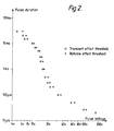
- Figure 3 depicts on a log log scale how the switching pulse duration varied as a function of switching voltage for an 8.9 ⁇ m thick layer of this F * phase material when maintained at a temperature of 124 o C.
- the dilution of the chiral dopant by the HEPTOBPD/TBBA mixture provided a pitch helix for the bulk material significantly longer (c.40 ⁇ m) than the layer thickness, and hence no pitch lines were seen in
- the ability to construct relatively fast switching bistable cells with a liquid crystal layer thickness significantly greater than 3 ⁇ m is advantageous because it means that much of the technology previously developed for other types of cell, such as twisted nematic and phase change cells, can now be expected to be applied with little modification to the manufacture of these cells; whereas rather more significant changes would likely to be required if the thickness range developed for those other types of cell had to be substantially reduced to bring the thickness beneath the 3 ⁇ m threshold.
- Transparent electrode layer 14 consists of a finely spaced set of rows or columns, while electrode layer 15 consists of a similar set extending in the orthogonal direction.
- the electrode rows and columns are made as narrow as conveniently possible, and similarly the inter-row and inter-column electrode spacings are also made as narrow as possible.
- the inter-pixel spacings are not significantly smaller than the widths of the pixels themselves, then it will generally be preferred to arrange for the inter-row and inter-column electrode spacings to be occupied by opaque material so that the modulated light, that is the light that passes through the pixels, is not swamped by the unmodulated light that would otherwise be able to pass through the areas between neighbouring pixels.
- the cell construction can incorporate an active silicon single crystal slice to replace the transparent rear sheet of a transmission type device.
- a sheet carries an array of metal pads whose members are connected with the drains of an associated array of FET's formed in the silicon, this array of FET's being accessed on a co-ordinate basis.
- the pixels of the cell are defined by the regions of the liquid crystal layer that lie between these pads and a transparent counter-electrode carried on the inward-facing surface of the transparent front sheet of the cell.
- Specular reflection at the rear of the liquid crystal layer is required over the areas registering with the pixels, and in some circumstances this may be provided by the reflective properties of the metal pads, but if the flatness is not adequate, then the whole surface may be coated with dielectric material to improve the flatness, and then a multilayer interference filter type reflector is deposited on top of that. Since the device works in reflective mode, the front sheet of the cell needs to be made of good optical quality glass and should be provided with an anti-reflection coating on its front surface.
- Linear arrays of pixels can also be used for two-dimensional OIP, for instance by having two linear arrays with one arranged side by side in the input plane and, in the Fourier transform plane, some means for recording the interference patterns of their Fourier transforms.
- a linear array can have a construction similar to the two-dimensional array, with the difference that, instead of having a set of column electrodes facing the row electrodes, the row electrodes are faced by a single large area counter-electrode. When particularly fine resolution is required the problem may arise of accessing the individual electrodes.
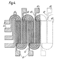
- One way of easing this problem is to employ a two-dimensional accessing for a one-dimensional pixel array. An example of such a system is illustrated in Figure 4.
- the sheet on one side of the liquid crystal layer carries a set of substantially rectangular transparent electrodes 40 which extend widthwise across the cell and are provided with terminal pads 41 and connecting links 42.
- the sheet on the other side of the liquid crystal layer carries a set of serpentine transparent electrodes 43 with terminal pads 44. In this instance four electrodes 43 are depicted. All the members of each loop register with each one of the rectangles 40 to define overlapping areas, the pixels, having the form of a regular array of uniformly spaced straight strips.
- the additional areas of overlap, where the connecting links 42 are overlapped by the serpentine electrodes 43 can conveniently be masked out with opaque matter if they prove a nuisance.
- the binary electro-optic effect provided by these cells can be employed in a unipolar mode, a bipolar mode, or a guest dyed unipolar mode.
- a transmission type cell In unipolar mode operation a transmission type cell is irradiated with an extended wavefront of linearly polarised coherent monochromatic light.
- the cell is arranged in relation to this polarisation plane so that in one of the cell states the liquid crystal director lies in that plane.
- the light transmitted by the cell then passes through a polarisation analyser, which is set with its polarisation plane in crossed relationship with the plane of polarisation of the light incident upon the cell.
- the birefringence and thickness of the liquid crystal layer within the cell are chosen so that it will function as a half wave retardation plate.
- the effect of energising of the cell is to rotate the fast axis of this half wave plate through the angle between the two director states of the cell.
- this angle is chosen to be near 45 o so that, with appropriate orientation of the cell, energisation produces a 90 o rotation of polarisation plane. It may be noted that in the I* and F* phases the angle between the director states is much less heavily dependent upon temperature than in the C* state, and therefore temperature regulation is not so critical.
- phase coding reduces the d.c. spot amplitude in the Fourier plane by destructive interference.
- the analyser is also dispensed with in the unipolar mode if a guest pleochroic dye is incorporated into the liquid crystal to give a guest dyed unipolar mode.
- the beam splitter is not a polarisation beam splitter, but is of conventional construction not intended to be polarisation sensitive.
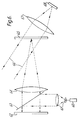
- Figures 5 and 6 depict respectively schematic representations of a joint transform correlator and of a frequency plane correlator which employ ferroelectric liquid crystal cells.
- plane polarised light from a laser 50 is beam expanded at 51 and directed on to a pair of reflex type I* or F* ferroelectric cells 52 via a polarisation beam splitter 53.
- One of the cells 52 carries the object data for correlation with the scene data carried by the other cell.
- a first Fourier transform lens 54 collects the reflected light and directs it to interfere in the Fourier transform plane where is located a recording device 55. For real-time correlation this may be for instance a bismuth silicon oxide detector.
- This recording device is interrogated with light from a second laser 56. Diffracted light is collected by a second Fourier transform lens 57 and directed to a photodetector 58 positioned in the Fourier transform plane.
- the resulting output from the detector is fed to a processing unit 59 for utilisation.
- plane polarised light from a laser 60 is beam expanded at 61 and directed on to a single reflex type I* or F* ferroelectric cell 62 via a polarisation beam splitter 63.
- a first Fourier transform lens 64 collects the reflected light and directs it to a recording device 65 positioned in the Fourier transform plane where it is interferred with a collimated reference beam 66.
- a second Fourier transform lens 67 is positioned to collect light that has been reflected by the cell 62 now programmed with alternative information, this light being such as to act on the stored information of the recording device to reconstruct the reference beam if there is correlation between the alternative information content of cell 62 and its original information content. This light collected by lens 67 is directed to a photodetector positioned in the correlation plane.
Landscapes
- Physics & Mathematics (AREA)
- Chemical & Material Sciences (AREA)
- Crystallography & Structural Chemistry (AREA)
- Nonlinear Science (AREA)
- General Physics & Mathematics (AREA)
- Optics & Photonics (AREA)
- Liquid Crystal (AREA)
- Image Analysis (AREA)
- Holo Graphy (AREA)
Claims (10)
- Eine Flüssigkristallzelle, die eine Betriebs-Bistabilität zeigt und eine smektische ferroelektrische I*- oder F*-Phasen-Flüssigkristallschicht aufweist, die zwischen gegenüberliegenden, mit Elektroden versehenen Platten eingeschlossen ist, dadurch gekennzeichnet, daß die Platten dazu dienen, eine Flüssigkristallschicht mit einer Dicke im Bereich von 4 - 40 Mikrometern auszubilden, und daß ihre nach innen gerichteten Oberflächen so behandelt sind, daß sie eine planare Ausrichtung der benachbarten Flüssigkristallmoleküle in der gleichen Richtung an jeder dieser beiden Oberflächen fördern.
- Zelle nach Anspruch 1, bei der die Flüssigkristallschichtdicke kleiner als 20 Mikrometer ist.
- Zelle nach Anspruch 1 oder 2, bei der ein pleochroider Farbstoff in der Flüssigkristallschicht dispergiert ist.
- Optisches Informationsverarbeitungsgerät, das zumindestens eine Flüssigkristallzelle nach Anspruch 1, 2 oder 3 enthält.
- Gerät nach Anspruch 4, bei dem die oder jede Zelle eine Zelle vom Transmissionstyp ist.
- Gerät nach Anspruch 4, bei dem die oder jede Zelle eine Zelle vom Reflektionstyp ist.
- Gerät nach Anspruch 4, 5 oder 6, bei dem die oder jede Zelle für einen Betrieb in einer unipolaren Betriebsart ausgebildet ist.
- Gerät nach Anspruch 4, 5 oder 6, bei dem die oder jede Zelle zum Betrieb in einer bipolaren Betriebsart ausgebildet ist.
- Gerät nach einem der Ansprüche 4 bis 8, wobei das Gerät ein Korrelator für eine gemeinsame Transformation ist.
- Gerät nach einem der Ansprüche 4 bis 8, wobei das Gerät ein Korrelator in der Frequenzebene ist.
Applications Claiming Priority (2)
| Application Number | Priority Date | Filing Date | Title |
|---|---|---|---|
| GB8428811 | 1984-11-14 | ||
| GB08428811A GB2166258B (en) | 1984-10-25 | 1984-11-14 | Two dimensional optical information processing apparatus |
Publications (3)
| Publication Number | Publication Date |
|---|---|
| EP0182509A2 EP0182509A2 (de) | 1986-05-28 |
| EP0182509A3 EP0182509A3 (en) | 1988-04-27 |
| EP0182509B1 true EP0182509B1 (de) | 1992-04-08 |
Family
ID=10569737
Family Applications (1)
| Application Number | Title | Priority Date | Filing Date |
|---|---|---|---|
| EP85307641A Expired EP0182509B1 (de) | 1984-11-14 | 1985-10-23 | Zweidimensionales optisches Informationsverarbeitungsgerät |
Country Status (6)
| Country | Link |
|---|---|
| US (1) | US4722594A (de) |
| EP (1) | EP0182509B1 (de) |
| JP (1) | JPS61122628A (de) |
| AT (1) | ATE74674T1 (de) |
| AU (1) | AU573402B2 (de) |
| DE (1) | DE3585820D1 (de) |
Families Citing this family (12)
| Publication number | Priority date | Publication date | Assignee | Title |
|---|---|---|---|---|
| GB8608116D0 (en) * | 1986-04-03 | 1986-05-08 | Secr Defence | Liquid crystal devices |
| ATE98381T1 (de) * | 1987-04-07 | 1993-12-15 | Hoechst Ag | Verwendung von verbindungen oder gemischen von verbindungen, die eine chirale, orthogonale, hoeher geordnete smektische phase aufweisen, im bereich dieser phase als schalt- oder anzeigemedium. |
| GB8726996D0 (en) * | 1987-11-18 | 1987-12-23 | Secr Defence | Multiplex addressing of ferro-electric liquid crystal displays |
| KR900018725A (ko) * | 1988-05-12 | 1990-12-22 | 야마자끼 순페이 | 액정 전자 광학 장치 |
| US5132811A (en) * | 1989-08-10 | 1992-07-21 | Seiko Instruments Inc. | Holographic operating optical apparatus |
| US5539555A (en) * | 1990-07-20 | 1996-07-23 | Displaytech, Inc. | High contrast distorted helex effect electro-optic devices and tight ferroelectric pitch ferroelectric liquid crystal compositions useful therein |
| US5233554A (en) * | 1990-09-10 | 1993-08-03 | United Technologies Corporation | Programmable optical correlator |
| US5216415A (en) * | 1990-12-19 | 1993-06-01 | Sumitomo Electric Industries, Ltd. | Method of driving a matrix-type liquid crystal display device |
| US5189294A (en) * | 1992-07-08 | 1993-02-23 | The United States Of America As Represented By The Secretary Of The Air Force | Transform lens with a plurality of sliced lens segments |
| US5400047A (en) * | 1993-11-10 | 1995-03-21 | Beesely; Dwayne E. | High brightness thin film electroluminescent display with low OHM electrodes |
| WO1995015513A1 (en) * | 1993-11-30 | 1995-06-08 | Isis Innovation Limited | Improvements relating to spatial light modulators |
| JP3455791B2 (ja) * | 1995-12-25 | 2003-10-14 | 独立行政法人産業技術総合研究所 | 光演算処理装置 |
Family Cites Families (15)
| Publication number | Priority date | Publication date | Assignee | Title |
|---|---|---|---|---|
| US3624605A (en) * | 1968-12-13 | 1971-11-30 | Honeywell Inc | Optical character recognition system and method |
| FR2499735A1 (fr) * | 1981-02-06 | 1982-08-13 | Thomson Csf | Dispositif optique transformateur de fourier et correlateur optique mettant en oeuvre ce dispositif optique transformateur de fourier |
| US4404555A (en) * | 1981-06-09 | 1983-09-13 | Northern Telecom Limited | Addressing scheme for switch controlled liquid crystal displays |
| DE3376692D1 (en) * | 1982-06-29 | 1988-06-23 | Secr Defence Brit | Liquid crystal devices |
| US4596446B2 (en) * | 1982-06-29 | 1997-03-18 | Secr Defence Brit | Liquid crystal devices with particular cholestric pitch-cell thickness ratio |
| GB2129954B (en) * | 1982-10-22 | 1986-03-05 | Stc Plc | Liquid crystal display device |
| GB2146473B (en) * | 1983-09-10 | 1987-03-11 | Standard Telephones Cables Ltd | Addressing liquid crystal displays |
| FR2557719B1 (fr) * | 1984-01-03 | 1986-04-11 | Thomson Csf | Dispositif de visualisation a memoire utilisant un materiau ferroelectrique |
| GB2154092A (en) * | 1984-02-07 | 1985-08-29 | Standard Telephones Cables Ltd | Optical correlator |
| GB2154331B (en) * | 1984-02-16 | 1987-07-01 | Standard Telephones Cables Ltd | Coherent light optical processor |
| JPS60188925A (ja) * | 1984-03-09 | 1985-09-26 | Canon Inc | 光学変調素子の製造法 |
| JPS60220316A (ja) * | 1984-04-16 | 1985-11-05 | Canon Inc | 液晶光学素子 |
| JPS6167836A (ja) * | 1984-09-11 | 1986-04-08 | Canon Inc | 液晶素子の駆動法 |
| JPS6170530A (ja) * | 1984-09-14 | 1986-04-11 | Canon Inc | 液晶素子の駆動法 |
| GB2166256B (en) * | 1984-10-25 | 1988-06-08 | Stc Plc | Ferroelectric liquid crystal display cells |
-
1985
- 1985-10-23 AT AT85307641T patent/ATE74674T1/de not_active IP Right Cessation
- 1985-10-23 EP EP85307641A patent/EP0182509B1/de not_active Expired
- 1985-10-23 DE DE8585307641T patent/DE3585820D1/de not_active Expired - Fee Related
- 1985-11-12 JP JP60253635A patent/JPS61122628A/ja active Pending
- 1985-11-13 AU AU49876/85A patent/AU573402B2/en not_active Ceased
- 1985-11-14 US US06/797,920 patent/US4722594A/en not_active Expired - Fee Related
Also Published As
| Publication number | Publication date |
|---|---|
| ATE74674T1 (de) | 1992-04-15 |
| US4722594A (en) | 1988-02-02 |
| DE3585820D1 (de) | 1992-05-14 |
| JPS61122628A (ja) | 1986-06-10 |
| AU4987685A (en) | 1986-05-22 |
| EP0182509A2 (de) | 1986-05-28 |
| AU573402B2 (en) | 1988-06-09 |
| EP0182509A3 (en) | 1988-04-27 |
Similar Documents
| Publication | Publication Date | Title |
|---|---|---|
| JP2548749B2 (ja) | マトリックスアドレス表示装置 | |
| US4902107A (en) | Ferroelectric liquid crystal optical device having temperature compensation | |
| EP0032362B1 (de) | Elektro-optische Vorrichtung mit einem chiralen smektischen Flüssigkristall und Verfahren zu ihrer Herstellung | |
| US5062691A (en) | Liquid crystal device with grey scale | |
| EP0182509B1 (de) | Zweidimensionales optisches Informationsverarbeitungsgerät | |
| US4529271A (en) | Matrix addressed bistable liquid crystal display | |
| US3687515A (en) | Electro-optic liquid crystal system with polyamide resin additive | |
| EP0166288B1 (de) | Bistabile Flüssigkristallspeichervorrichtung | |
| HK44096A (en) | Ferroelectric liquid-crystal cell | |
| GB2166258A (en) | Two dimensional optical information processing apparatus | |
| EP0281341B1 (de) | Flexoelektrische Flüssigkristallvorrichtung | |
| EP0250218B1 (de) | Flüssigkristallvorrichtungen | |
| EP0103170B1 (de) | Informationsfesthaltungsanordnung | |
| EP0251639B1 (de) | Flüssigkristallzelle | |
| US3854751A (en) | Method for rapidly switching a display by sequential application of orthogonal electric fields to a liquid crystal material having optical properties of the nematic mesophase | |
| KR100218127B1 (ko) | 그레이 스케일을 갖는 액정 디바이스 | |
| US4799775A (en) | Ferroelectric liquid crystal cells having a helical liquid crystal structure | |
| CA1191587A (en) | Thermally addressed liquid crystal device | |
| HK1007806B (en) | Liquid crystal device with grey scale | |
| Sussman | Electrooptic liquid crystal devices: principles and applications | |
| US5841503A (en) | High molecular liquid crystal device and method of manufacturing the same | |
| Pasko et al. | Liquid crystal infrared modulation | |
| CA1304485C (en) | Liquid crystal display element and method for driving same | |
| Thurston | Liquid Crystal Bistable Displays | |
| JP2727239B2 (ja) | 強誘電性液晶素子 |
Legal Events
| Date | Code | Title | Description |
|---|---|---|---|
| PUAI | Public reference made under article 153(3) epc to a published international application that has entered the european phase |
Free format text: ORIGINAL CODE: 0009012 |
|
| AK | Designated contracting states |
Kind code of ref document: A2 Designated state(s): AT BE CH DE FR IT LI LU NL SE |
|
| RAP1 | Party data changed (applicant data changed or rights of an application transferred) |
Owner name: STC PLC |
|
| PUAL | Search report despatched |
Free format text: ORIGINAL CODE: 0009013 |
|
| AK | Designated contracting states |
Kind code of ref document: A3 Designated state(s): AT BE CH DE FR IT LI LU NL SE |
|
| 17P | Request for examination filed |
Effective date: 19880609 |
|
| 17Q | First examination report despatched |
Effective date: 19900824 |
|
| GRAA | (expected) grant |
Free format text: ORIGINAL CODE: 0009210 |
|
| RAP1 | Party data changed (applicant data changed or rights of an application transferred) |
Owner name: NORTHERN TELECOM LIMITED |
|
| AK | Designated contracting states |
Kind code of ref document: B1 Designated state(s): AT BE CH DE FR IT LI LU NL SE |
|
| PG25 | Lapsed in a contracting state [announced via postgrant information from national office to epo] |
Ref country code: SE Effective date: 19920408 Ref country code: NL Effective date: 19920408 Ref country code: LI Effective date: 19920408 Ref country code: IT Free format text: LAPSE BECAUSE OF FAILURE TO SUBMIT A TRANSLATION OF THE DESCRIPTION OR TO PAY THE FEE WITHIN THE PRESCRIBED TIME-LIMIT;WARNING: LAPSES OF ITALIAN PATENTS WITH EFFECTIVE DATE BEFORE 2007 MAY HAVE OCCURRED AT ANY TIME BEFORE 2007. THE CORRECT EFFECTIVE DATE MAY BE DIFFERENT FROM THE ONE RECORDED. Effective date: 19920408 Ref country code: CH Effective date: 19920408 Ref country code: BE Effective date: 19920408 Ref country code: AT Effective date: 19920408 |
|
| REF | Corresponds to: |
Ref document number: 74674 Country of ref document: AT Date of ref document: 19920415 Kind code of ref document: T |
|
| ET | Fr: translation filed | ||
| REF | Corresponds to: |
Ref document number: 3585820 Country of ref document: DE Date of ref document: 19920514 |
|
| REG | Reference to a national code |
Ref country code: CH Ref legal event code: PL |
|
| NLV1 | Nl: lapsed or annulled due to failure to fulfill the requirements of art. 29p and 29m of the patents act | ||
| PG25 | Lapsed in a contracting state [announced via postgrant information from national office to epo] |
Ref country code: LU Free format text: LAPSE BECAUSE OF NON-PAYMENT OF DUE FEES Effective date: 19921031 |
|
| PGFP | Annual fee paid to national office [announced via postgrant information from national office to epo] |
Ref country code: DE Payment date: 19921230 Year of fee payment: 8 |
|
| PLBE | No opposition filed within time limit |
Free format text: ORIGINAL CODE: 0009261 |
|
| STAA | Information on the status of an ep patent application or granted ep patent |
Free format text: STATUS: NO OPPOSITION FILED WITHIN TIME LIMIT |
|
| 26N | No opposition filed | ||
| PGFP | Annual fee paid to national office [announced via postgrant information from national office to epo] |
Ref country code: FR Payment date: 19930909 Year of fee payment: 9 |
|
| PG25 | Lapsed in a contracting state [announced via postgrant information from national office to epo] |
Ref country code: DE Effective date: 19940701 |
|
| PG25 | Lapsed in a contracting state [announced via postgrant information from national office to epo] |
Ref country code: FR Effective date: 19950630 |
|
| REG | Reference to a national code |
Ref country code: FR Ref legal event code: ST |