EP0182664A2 - Oszillator mit geringem Rauschen - Google Patents
Oszillator mit geringem Rauschen Download PDFInfo
- Publication number
- EP0182664A2 EP0182664A2 EP85308458A EP85308458A EP0182664A2 EP 0182664 A2 EP0182664 A2 EP 0182664A2 EP 85308458 A EP85308458 A EP 85308458A EP 85308458 A EP85308458 A EP 85308458A EP 0182664 A2 EP0182664 A2 EP 0182664A2
- Authority
- EP
- European Patent Office
- Prior art keywords
- oscillator
- input
- inverting
- output
- noise
- Prior art date
- Legal status (The legal status is an assumption and is not a legal conclusion. Google has not performed a legal analysis and makes no representation as to the accuracy of the status listed.)
- Ceased
Links
Images
Classifications
-
- H—ELECTRICITY
- H03—ELECTRONIC CIRCUITRY
- H03B—GENERATION OF OSCILLATIONS, DIRECTLY OR BY FREQUENCY-CHANGING, BY CIRCUITS EMPLOYING ACTIVE ELEMENTS WHICH OPERATE IN A NON-SWITCHING MANNER; GENERATION OF NOISE BY SUCH CIRCUITS
- H03B5/00—Generation of oscillations using amplifier with regenerative feedback from output to input
- H03B5/18—Generation of oscillations using amplifier with regenerative feedback from output to input with frequency-determining element comprising distributed inductance and capacitance
- H03B5/1805—Generation of oscillations using amplifier with regenerative feedback from output to input with frequency-determining element comprising distributed inductance and capacitance the frequency-determining element being a coaxial resonator
-
- H—ELECTRICITY
- H03—ELECTRONIC CIRCUITRY
- H03B—GENERATION OF OSCILLATIONS, DIRECTLY OR BY FREQUENCY-CHANGING, BY CIRCUITS EMPLOYING ACTIVE ELEMENTS WHICH OPERATE IN A NON-SWITCHING MANNER; GENERATION OF NOISE BY SUCH CIRCUITS
- H03B2202/00—Aspects of oscillators relating to reduction of undesired oscillations
- H03B2202/01—Reduction of undesired oscillations originated from distortion in one of the circuit elements of the oscillator
- H03B2202/012—Reduction of undesired oscillations originated from distortion in one of the circuit elements of the oscillator the circuit element being the active device
-
- H—ELECTRICITY
- H03—ELECTRONIC CIRCUITRY
- H03B—GENERATION OF OSCILLATIONS, DIRECTLY OR BY FREQUENCY-CHANGING, BY CIRCUITS EMPLOYING ACTIVE ELEMENTS WHICH OPERATE IN A NON-SWITCHING MANNER; GENERATION OF NOISE BY SUCH CIRCUITS
- H03B2202/00—Aspects of oscillators relating to reduction of undesired oscillations
- H03B2202/02—Reduction of undesired oscillations originated from natural noise of the circuit elements of the oscillator
- H03B2202/025—Reduction of undesired oscillations originated from natural noise of the circuit elements of the oscillator the noise being coloured noise, i.e. frequency dependent noise
- H03B2202/027—Reduction of undesired oscillations originated from natural noise of the circuit elements of the oscillator the noise being coloured noise, i.e. frequency dependent noise the noise being essentially proportional to the inverse of the frequency, i.e. the so-called 1/f noise
Definitions
- This invention relates to low noise oscillators, particularly microwave oscillators employing a gallium arsenide field-effect transistor as an amplifying element.
- the gallium arsenide field-effect transistor (GaAs FET) is especially suitable for use as a microwave amplifier because its parameters are relatively less variable as a function of operating conditions and its impedance is generally higher than in comparable bipolar devices. This results in wider bandwidth, lower noise, and higher linearity.
- GaAs FET gallium arsenide field-effect transistor
- a problem is encountered in the use of a GaAs FET as an oscillator due to characteristic noise that is inordinately high in the GaAs FET.
- This noise which is generated primarily between the gate and the source of the FET, is in addition to normal thermal noise generated in all circuits.
- the aforementioned characteristic noise is of little concern where a GaAs FET is used as a linear microwave amplifier, since the noise is easily filtered out by a high pass filter, in an oscillator it results in spectral impurity of the output.
- the amplifying element of an oscillator ordinarily performs a limiting function to maintain the oscillator signal at constant amplitude.
- the limiting function necessarily causes the amplifier to operate to some degree in a non-linear manner; hence, modulation of the oscillation signal by the noise signal components occurs.
- the oscillator output includes noise sidebands whose amplitudes vary inversely with the difference in frequency between the frequency of oscillation and the frequency of the examination.
- the present invention provides an oscillator circuit configuration wherein the amplitude limiting function of the oscillator is divorced from the amplifying function.
- a GaAs FET amplifier is operated in the linear mode.
- a limiting circuit is placed in the oscillator's feedback circuit and separated from the amplifier by a high pass filter which allows the high frequency oscillation signal to be fed back to the input of the amplifier while blocking the low frequency noise produced by the FET from reaching the limiting circuit and modulating the oscillation signal.
- the GaAs FET amplifier is provided with a resistive biasing load connected from the FET drain to the supply voltage.
- the drain is also capacitively coupled to a tuned circuit, or resonator, which is also capacitively coupled to the gate of the FET, thereby providing positive feedback at the frequency of oscillation.
- a resistor is connected from the gate to supply common for input biasing.
- a diode bridge limiting circuit is coupled from supply common to the source of the FET through a capacitor. Positive and negative current limits on the amplitude of the signal are provided by connecting the bridge to respective reference voltages through respective resistors.
- the source is also connected to supply common through an inductor. The capacitor between the source and the limiter and the inductor between the source and supply common serve as a high pass filter blocking the characteristic FET noise.
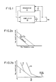
- a conventional microwave oscillator employs an amplifier 10 having a feedback loop 12 including a resonator 14 for providing positive feedback at the frequency of oscillation. That is, at that frequency the feedback through the resonator is maximized and in phase with the input signal to the amplifier.
- the amplitude of the oscillation signal is limited by the amplifier itself, the open loop gain of the amplifier and feedback circuit being greater than one in order to start and sustain oscillation in a practical circuit.
- the amplifier must, to some degree, operate in a non-linear manner. As a result, any signal components, such as noise, passing through the amplifier will modulate the oscillation signal, resulting in a signal-at output 16 having unwanted frequency components, that is, noise sidebands.
- the amplitude of characteristic noise produced by a gallium arsenide field-effect transistor as a function of the frequency of examination is compared to the amplitude of characteristic noise produced by a bipolar transistor.
- the additional noise produced by a GaAs FET is typically about 20dB higher than for a bipolar transistor.
- the amplitude of the characteristic noise is approximately inversely proportional to the frequency of examination; thus, it drops off at about 3dB per octave.
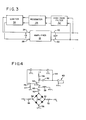
- the oscillator of the present invention employs an amplifier 18 biased to operate at all times in a linear mode.
- the amplifier is provided with an output port having an inverting output 20 and a non-inverting output 22. It is also provided with an input port having an inverting input 24 and a reference input 26.
- the amplitude of the inverting output 20 changes inversely in relation to the inverting input 24.
- the invention is directed to the use of an amplifying element comprising a GaAs FET because of the noise characteristics peculiar to that device, it is to be recognized that other amplifying devices might be employed advantageously without departing from the principles of the invention.
- Positive feedback at the frequency of oscillation of the amplifier in order to sustain oscillation is produced by a resonator, or tuned circuit, 28.
- the resonator produces a 180 degree phase shift in the feedback signal so that the feedback signal is in phase with the input to the amplifier; that is, if the feedback loop were opened at the input to the amplifier and a signal at the frequency of oscillation were applied to the input, the output from the resonator 22 would be in phase with that signal.
- the resonator also ensures that the feedback signal is at a maximum only at that frequency.
- the oscillator is provided with an amplitude limiter 30. Because the limiter places a limit on the amplitude of the signal passing through it, the circuit is necessarily non-linear.
- the oscillator is provided with a high pass filter 32. Since the characteristic noise decreases with frequency, it is only relatively low frequency noise that is of practical concern.
- the high pass filter blocks characteristic noise produced by the amplifier 18 from reaching the limiter 30, and thereby prevents the limiter from modulating the input to the amplifier by that noise. It is to be understood that the limiter 30 may be placed anywhere in the feedback loop, provided that a high pass filter is provided to prevent low frequency noise from reaching the limiter.
- the amplifier comprises a GaAs FET 34, having a biasing load resistor 36 connected from a positive power supply to the drain D of the FET, an input biasing resistor 37 connected from the gate G to power supply common, and an inductor 38 connected from the source S to power supply common.
- the gate of the FET may be viewed as an inverting input to the amplifier, the power supply common as a reference input to the amplifier, the drain of the FET as the inverting output of the amplifier, and the source of the FET as the non-inverting output of the amplifier.
- the resonator 40 typically comprises a loop device having capacitive and inductive characteristics of a tuned circuit. It is coupled to the drain of the FET by a capacitor 42 and to the gate of the FET by a capacitor 46, so as to avoid interference with the DC biasing of the transistor.
- the limiter is placed in the non-inverting loop of the feedback circuit.
- the limiter comprises a conventional limiter having four diodes 48 in a bridge configuration.
- the top 50 of the bridge is connected through a resistor 52 to a positive limiting voltage +V L and the bottom 54 of the bridge is connected through a resistor 56 to a negative limiting voltage -V L -
- the diodes 48 are therefore ordinarily forward biased.
- a first side 58 of the bridge is connected to supply common and the other side 60 of the bridge is coupled through a capacitor 62 to the source, or non-inverting output, of the FET. Capacitor 62 prevents the bridge from interferring with the DC biasing of the transistor.
- Resistors 52 and 56 have relatively high resistance, e.g. 15 K ohms, as compared to the forward biased impedance of the diodes, e.g. about 54 ohms.
- Resistors 52 and 56 have relatively high resistance, e.g. 15 K ohms, as compared to the forward biased impedance of the diodes, e.g. about 54 ohms.
- the object is to prevent that noise from reaching the input through the non-inverting feedback loop. This is accomplished by capacitor 62 and an inductor 38, connected between the source and power supply common, which not only isolate the DC biasing from the AC signal path, but act as a high pass filter to prevent the low-frequency characteristic noise generated at the source from reaching the limiter and modulating the oscillator signal.
Landscapes
- Inductance-Capacitance Distribution Constants And Capacitance-Resistance Oscillators (AREA)
Applications Claiming Priority (2)
| Application Number | Priority Date | Filing Date | Title |
|---|---|---|---|
| US674210 | 1984-11-23 | ||
| US06/674,210 US4580109A (en) | 1984-11-23 | 1984-11-23 | Low noise oscillator |
Publications (2)
| Publication Number | Publication Date |
|---|---|
| EP0182664A2 true EP0182664A2 (de) | 1986-05-28 |
| EP0182664A3 EP0182664A3 (de) | 1987-12-02 |
Family
ID=24705753
Family Applications (1)
| Application Number | Title | Priority Date | Filing Date |
|---|---|---|---|
| EP85308458A Ceased EP0182664A3 (de) | 1984-11-23 | 1985-11-20 | Oszillator mit geringem Rauschen |
Country Status (4)
| Country | Link |
|---|---|
| US (1) | US4580109A (de) |
| EP (1) | EP0182664A3 (de) |
| JP (1) | JPS61131603A (de) |
| CA (1) | CA1261411A (de) |
Families Citing this family (6)
| Publication number | Priority date | Publication date | Assignee | Title |
|---|---|---|---|---|
| FR2595518A1 (fr) * | 1986-03-07 | 1987-09-11 | Thomson Csf | Oscillateur a faible bruit aux environs de sa frequence d'oscillation |
| US4797639A (en) * | 1987-05-22 | 1989-01-10 | The United States Of America As Represented By The Secretary Of The Air Force | Low noise crystal controlled oscillator |
| US4785263A (en) * | 1987-05-28 | 1988-11-15 | Motorola, Inc. | FET oscillator circuit |
| US6362695B1 (en) * | 1999-12-21 | 2002-03-26 | Intel Corporation | Method and apparatus to produce a random bit sequence |
| US6489853B1 (en) | 2002-03-19 | 2002-12-03 | Z-Communications, Inc. | Low phase noise oscillator |
| US8054137B2 (en) * | 2009-06-09 | 2011-11-08 | Panasonic Corporation | Method and apparatus for integrating a FLL loop filter in polar transmitters |
Family Cites Families (5)
| Publication number | Priority date | Publication date | Assignee | Title |
|---|---|---|---|---|
| DE1295681B (de) * | 1964-02-13 | 1969-05-22 | Siemens Ag | Oszillator mit einem Amplitudenbegrenzer im Ausgangskreis |
| FR2044275A5 (de) * | 1969-05-14 | 1971-02-19 | Constr Telephoniques | |
| US3996530A (en) * | 1975-06-30 | 1976-12-07 | International Business Machines Corporation | Butler oscillator |
| DE3003302C2 (de) * | 1980-01-30 | 1982-12-23 | Siemens AG, 1000 Berlin und 8000 München | Stromgesteuerter Oszillator |
| JPS60172805A (ja) * | 1984-01-30 | 1985-09-06 | Nippon Telegr & Teleph Corp <Ntt> | コイル励磁用発振回路 |
-
1984
- 1984-11-23 US US06/674,210 patent/US4580109A/en not_active Expired - Fee Related
-
1985
- 1985-11-18 CA CA000495571A patent/CA1261411A/en not_active Expired
- 1985-11-20 EP EP85308458A patent/EP0182664A3/de not_active Ceased
- 1985-11-21 JP JP60262358A patent/JPS61131603A/ja active Pending
Also Published As
| Publication number | Publication date |
|---|---|
| EP0182664A3 (de) | 1987-12-02 |
| JPS61131603A (ja) | 1986-06-19 |
| CA1261411A (en) | 1989-09-26 |
| US4580109A (en) | 1986-04-01 |
Similar Documents
| Publication | Publication Date | Title |
|---|---|---|
| US5130675A (en) | Voltage-controlled oscillator | |
| CA1303679C (en) | Modulator and transmitter | |
| US4462004A (en) | Dynamic class-4 FET amplifier | |
| US7907073B2 (en) | Variable passive components with high resolution value selection and control | |
| US5822685A (en) | Modulating reflector circuit | |
| CA1047613A (en) | Butler oscillator | |
| US4158182A (en) | Low noise oscillator circuit | |
| US4705967A (en) | Multifunction floating FET circuit | |
| US3443241A (en) | High level rf transistor distortion correction circuit | |
| US5192875A (en) | Analog frequency divider utilizing two amplifiers and a LC resonant circuit | |
| US4580109A (en) | Low noise oscillator | |
| JPS6115426A (ja) | ミキサ装置 | |
| US4626802A (en) | GaAs FET oscillator noise reduction circuit | |
| US4044308A (en) | Communication transmitting apparatus with carrier level control | |
| JPH05259766A (ja) | 可変利得増幅器を具える集積回路 | |
| US5459438A (en) | Negative feedback frequency stabilized pulse oscillator | |
| US3958190A (en) | Low harmonic crystal oscillator | |
| US6181217B1 (en) | VCXO with reduced PWM effects high slew rate conditions | |
| US3460056A (en) | Voltage tunable l-c oscillator with amplitude limited positive feedback | |
| EP0715404B1 (de) | Hochfrequenzverstärkungsschaltung | |
| US3461395A (en) | Amplifier circuits employing varactors for controlling power gain and bandwidth | |
| US4977379A (en) | Differential pair, push-push oscillator | |
| JPS6228607B2 (de) | ||
| Divina et al. | Experimental verification of a distributed amplifier oscillator | |
| JPH11195935A (ja) | 高周波集積回路装置 |
Legal Events
| Date | Code | Title | Description |
|---|---|---|---|
| PUAI | Public reference made under article 153(3) epc to a published international application that has entered the european phase |
Free format text: ORIGINAL CODE: 0009012 |
|
| AK | Designated contracting states |
Kind code of ref document: A2 Designated state(s): DE FR GB NL |
|
| PUAL | Search report despatched |
Free format text: ORIGINAL CODE: 0009013 |
|
| AK | Designated contracting states |
Kind code of ref document: A3 Designated state(s): DE FR GB NL |
|
| 17P | Request for examination filed |
Effective date: 19880127 |
|
| 17Q | First examination report despatched |
Effective date: 19890908 |
|
| RAP1 | Party data changed (applicant data changed or rights of an application transferred) |
Owner name: TEKTRONIX, INC. |
|
| STAA | Information on the status of an ep patent application or granted ep patent |
Free format text: STATUS: THE APPLICATION HAS BEEN REFUSED |
|
| 18R | Application refused |
Effective date: 19900916 |
|
| RIN1 | Information on inventor provided before grant (corrected) |
Inventor name: LOCKWOOD, LARRY R. |