EP0182715A2 - Appareil d'entrée de coordonnées - Google Patents
Appareil d'entrée de coordonnées Download PDFInfo
- Publication number
- EP0182715A2 EP0182715A2 EP85402221A EP85402221A EP0182715A2 EP 0182715 A2 EP0182715 A2 EP 0182715A2 EP 85402221 A EP85402221 A EP 85402221A EP 85402221 A EP85402221 A EP 85402221A EP 0182715 A2 EP0182715 A2 EP 0182715A2
- Authority
- EP
- European Patent Office
- Prior art keywords
- coordinate
- input
- correction
- transparent
- signals
- Prior art date
- Legal status (The legal status is an assumption and is not a legal conclusion. Google has not performed a legal analysis and makes no representation as to the accuracy of the status listed.)
- Granted
Links
Images







Classifications
-
- G—PHYSICS
- G06—COMPUTING OR CALCULATING; COUNTING
- G06F—ELECTRIC DIGITAL DATA PROCESSING
- G06F3/00—Input arrangements for transferring data to be processed into a form capable of being handled by the computer; Output arrangements for transferring data from processing unit to output unit, e.g. interface arrangements
- G06F3/01—Input arrangements or combined input and output arrangements for interaction between user and computer
- G06F3/03—Arrangements for converting the position or the displacement of a member into a coded form
- G06F3/041—Digitisers, e.g. for touch screens or touch pads, characterised by the transducing means
- G06F3/045—Digitisers, e.g. for touch screens or touch pads, characterised by the transducing means using resistive elements, e.g. a single continuous surface or two parallel surfaces put in contact
Definitions
- the present invention relates to a transparent coordinate input device that can be used overlapping the screen of a display unit.
- coordinate input devices are commercially available. They can be classified into pressure conductive-resistive type, static coupling type, and electromagnetic induction type devices in accordance with input position detection techniques.
- a conventional static coupling type coordinate input device uses a resistor plate with a large number of x- and y-coordinate electrodes in a peripheral region thereof and an insulating plate formed on the resistor plate. An AC voltage is applied to the electrodes of the resistor plate along the x and y directions. When an operator touches any point of the insulating plate with an input pen, an AC voltage is induced by static coupling in the input pen and the x- and y-coordinates can be detected.
- the static coupling type coordinate input device requires a complicated detector since AC voltage is used. Furthermore, input detection errors tend to occur due to a body effect, thereby distorting the image on the display screen.
- a conventional electromagnetic induction type coordinate input device uses a large number of x and y parallel conductor loops orthogonal to each other. When the operator touches any point with an electromagnetic input pen supplied with an AC current, a voltage is induced at the x and y conductor loops near the input point. A maximum value of the induction voltage is detected to determine the x- and y-coordinates of the input point.
- a conventional input device of this type also requires a complicated voltage detector. In addition, detection errors tend to occur due to holding the electromagnetic input pen at an improper angle, resulting in distortion on the display screen.
- a conventional pressure conductive-resistive type coordinate input device uses an input structure obtained by sequentially stacking a square resistor film, a pressure conductive rubber sheet, and a metal conductive film.
- the square resistor film has a large number of x- and y-coordinate detection electrodes on the respective sides thereof.
- the pressure conductive rubber sheet is rendered conductive when pressure is applied.
- a constant current source is connected to the conductive layer and the electrodes. When the operator touches any point (i.e., an input point) of the conductive layer with an input pen, the portion of the pressure conductive rubber sheet corresponding to the input point is rendered conductive.
- At least one of the current components flowing to the detection electrodes of the opposing sides with respect to the input point is detected, so that the x- and y-coordinates of the input point can be detected.
- the x- and y-coordinates of the input point can be easily detected as compared with the devices described above.
- the following drawbacks are also present.
- An input graphic or character pattern is displayed on a display unit, such as a CRT, that is external to the coordinate display device.
- a display unit such as a CRT
- the operator must change the field of view from the input surface to the display screen to check whether or not the input pattern has been properly entered. Therefore, effective man-machine interface cannot be achieved, and input is cumbersome and time-consuming.
- a constant current from a single contact current source is shunted from the input point to a pair of opposing electrodes.
- One of the shunted current components is measured by a detection resistor and an operational amplifier.
- the current to be measured is supplied to a detection resistor having a resistance sufficiently smaller than that of the resistor film.
- a voltage drop across the ends of the detection resistor is amplified by the operational amplifier to measure current.
- the detection resistor cannot have a high resistance, and thus the voltage drop across the ends of the resistor is small. In this sense, the operational amplifier must have a large gain and is thus sensitive to external noise.
- coordinate detection precision is determined solely by the sheet resistance of the resistor film.
- the input points are distorted on the display screen.
- a principal object of the present invention to solve the conventional problems described above and to provide a high-precision transparent coordinate input device with a transparent coordinate input panel which can be used overlapping the screen of a display unit or can be coupled together with the display unit.
- a coordinate input panel in a transparent coordinate input device comprises: a transparent insulating substrate, a flat square transparent resistor film formed on the substrate, and detection electrodes electrically connected to the sides of the transparent resistor film to allow a current flow along one of flow-in and flow-out directions with respect to the transparent resistor film.
- the coordinate input panel has a structure wherein a transparent protective layer with a planar resistance sufficiently higher than that along the direction of thickness thereof is formed on the upper surface of the transparent resistor film, thereby preventing damage to the transparent resistor film when it is touched by an electrical pen.
- the transparent input device of the present invention comprises: a power source circuit, electrically connected to an electrical pen, for supplying a drive current to the transparent resistor film from an input position; and detecting means, connected to the detection electrodes, for detecting the x- and y-coordinates of the input position specified by the electrical pen.
- the power source circuit comprises a drive voltage power source, one end of which is connected to the electrical pen, and a pair of constant-current circuits for maintaining currents flowing from the input position to the pair of detection electrodes at a constant value.
- the detecting means comprises a pair of operation circuits for detecting a potential difference between the opposing detection electrodes and for generating a signal representing the input position specified by the electrical pen.
- a transparent coordinate input device comprising correcting means for correcting an input position detection error, namely, the difference between the input position specified by the electrical pen and the detection position obtained by the detecting means.
- the correcting means comprises a coordinate correction table, for storing data needed for correcting an input position detection error, and operating means for correcting the error by retrieving data from the coordinate correction table.
- correction data is not prepared for all points, but rather for a small number of representative points. Correction is performed using the correction data of the representative point nearest the input position.
- a typical arrangement comprising a correction table for storing correction data of representative points is accessed such that a plurality of upper bits of the coordinates O x and O y are used as address data.
- a'converter to convert the detected coordinates O and 0 to the coordinates of the nearest x y representative point.
- the converter comprises an offset table for storing an offset value, representing the distance between the detected position and the corresponding representative point, and a subtracter for reading out the corresponding offset value from the offset table, subtracting the corresponding offset value from the coordinates O x and O y , and generating addresses at which the correction data of the nearest representative point is generated.
- a correction table for storing correction data representing a plurality of the nearest representative points and data representing differences between the correction data, and an interpolation circuit for performing interpolation with these data.
- a transparent coordinate input display device having correction data input means for easily and accurately entering correction data in the coordinate correction table, wherein a coordinate input unit is integrally coupled to a coordinate display unit.
- the correction data input means comprises a coordinate generator for generating digital coordinate data, means for causing the coordinate display unit to display a coordinate represented by an output from the coordinate generator, an operation circuit for calculating coordinate data detected by the coordinate input unit and the coordinate data generated by the coordinate generator to obtain coordinate correction data when the position.displayed on the display unit is touched by the electrical pen, and means for storing an output from the operation circuit in the coordinate correction table.
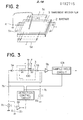
- Fig. 1 shows a coordinate input device according to an embodiment of the present invention
- Fig. 2 is a perspective view of a coordinate input panel 1.
- the coordinate input panel 1 comprises a substrate 2 of transparent glass, plastic or the like, a transparent resistor film 3 formed on the substrate 2, and detection electrodes 5a, 5b, 5c and 5d respectively connected to four sides of the transparent resistor film 3.
- the major surface of the resistor film 3 serves as an input surface.
- the transparent resistor film 3 is formed such that an S n 0 2 or IOT material is deposited by-CVD (Chemical Vapor Deposition) or by spraying, so as to obtain a uniform resistance throughout the surface of the film.
- CVD Chemical Vapor Deposition
- the transparent resistor film 3 0 has a thickness of, for example, about 500 A. In this case, sheet resistance is about 100 to 200 ⁇ /cm 2 .
- the detection electrodes 5a, 5b, 5c and 5d include diodes for preventing feedback of the current to the transparent resistor film 3. Cathodes of the plurality of diodes are spaced equidistantly (e.g., at intervals of 2 mm) and are connected by a conductive adhesive to the periphery of the transparent resistor film 3. The anodes of the diodes in the respective detection electrodes 5a, 5b, 5c and 5d are commonly connected.
- Constant current sources 8a and 8b are connected between the detection electrode 5a and ground by a switch 7a and between the detection electrode 5b and ground by a switch 7c, respectively.
- the detection electrodes 5c and 5d are grounded through switches 7a and 7c and the constant current sources 8a and 8b, respectively.
- Operational amplifiers 9a and 9b are connected between the detection electrodes 5c and 5d and between the detection electrodes 5a and 5b, respectively.
- the operational amplifiers 9a and 9b detect corresponding potential differences and amplify the potential differences.
- the amplified potential differences are supplied as y- and x-coordinates of the input point to sample-hold circuits 10a and 10b, respectively.
- a detection control circuit 11 alternately operates the pair of switches 7a and 7b and the pair of switches 7c and 7d. In synchronism with this switching, the sample-hold circuits 10a and 10b perform a sample-hold operation.
- a detection discriminator 26 comprises a comparator 24 and a reference power source 25. The detection discriminator 26 is included in the operational amplifiers 9a and 9b. In the detection discriminator 26, the comparator 24 compares potentials at the detection electrodes 5a and 5d with a voltage E l of the reference power source 25. When the potential at the detection electrode 5a or 5d exceeds the voltage E 1 , the comparator 24 generates a Z signal of "H" level. When the Z signal is set at "H" level, the discriminator 26 determines that an input (depression) has been made. In this case, input x- and y-coordinate signals are detected as significant data, thereby preventing input errors in the computer.
- Fig. 3 is an equivalent circuit for explaining the operation of the device shown in Fig. 1.
- an electrical pen 20 is in electrical contact with the transparent resistor film 3 at an input point, so that the switches 7a and 7c are closed while the switches 7b and 7d are opened.
- the circuit shows an operation state wherein an x-coordinate is detected.
- the voltage V is proportional to the resistance of the resistor R 1 .
- the resistance of the resistor R 1 is proportional to a distance x between the input position and the detection electrode 5a. Therefore, the voltage V is obtained as a value proportional to the distance x.
- the x-coordinate signal is held in the sample-hold circuit 10b while the y-coordinate is being detected (i.e., the switches 7a and 7c are opened and the switches 7b and 7d are closed).
- the detection electrodes are arranged at four sides of the transparent resistor film formed on the input surface, and currents flowing through the detection electrodes are kept constant upon application of the drive voltage thereto, so that x-and y-coordinates of the input point can be detected on the basis of the potential differences between the opposing detection electrodes. Therefore, the detection operation is substantially free from external noise, and high-precision position detection can be reliably performed.
- Fig. 4 is a sectional view showing another arrangement of a coordinate input panel (i.e., a transparent drawing pad) 1.
- a transparent protective film 6 is formed on the transparent resistor film 3 of Fig. 2.
- the resistance of the transparent protective film 6 along its thickness is sufficiently smaller (1/100 or less) than the planar resistance thereof.
- the transparent protective film is obtained by embedding conductive wires in a transparent polymer along a longitudinal direction thereof. Since a current flows only along the longitudinal direction, an electrical pen 20 is brought into contact with the surface of the transparent protective film 6, a current flows in the transparent resistor film 3 and then the electrodes 5a and 5b, thereby detecting x- and y-coordinates of the input point.
- the conductive wire may be replaced with carbon fiber, conductive fabric or metallic powder.
- Fig. 5 shows a transparent protective film 6' having a higher resistance than the transparent resistor film 3.
- a transparent pressure conductive sheet 6" may be used in place of the transparent protective films 6 and 6' on the coordinate input panels 1 of Figs. 4 and 5.
- the transparent pressure conductive sheet 6" is rendered electrically conductive along its thickness at an input point when a pressure of a predetermined value or more is applied to the input point.
- Transparent coordinate input devices for correcting such detection errors and performing high-precision input according to other embodiments of the present invention will be described hereinafter.
- Fig. 7 is a block diagram of a correction circuit with a correction table for storing correction data representing the relationship between coordinates I x and I y of an input position and detected coordinates O x and O y .
- An input position detector 36 corresponds to the device shown in Fig. 1.
- the correction circuit includes amplifiers 37 x and 37y for amplifying x- and y-coordinates detected by the input position detector 36, sample-hold circuits 38 x and 38y for sampling and holding outputs from the amplifiers 37 and 37 , respectively, A/D converters 39 x and 39y for converting analog outputs from the sample-hold circuits 38 x and 38 y , respectively, to digital signals, and x- and y-coordinate correction tables 40x and 40y for correcting outputs from the A/D converters 39 x and 39y, respectively.
- x- and y-coordinate signals detected by the input position detector 36 are amplified by the amplifiers 37 x and 37 y to a predetermined level. Amplified outputs are sampled and held by the sample-hold circuits 38 x and 38 y . The analog x- and y-coordinate signals are then converted by the A/D converters 39 x and 39y to digital signals. Finally, the digital x- and y-coordinate signals are supplied to the x- and y-coordinate correction tables 40 x and 40y to generate x- and y-coordinate signals corrected in correspondence with the digital x- and y-coordinate signals.
- Fig. 8 shows the relationship between the x-coordinate signal and the correction table.
- reference numeral 41 denotes a characteristic curve showing the relationship between the x-coordinate input position detected by the input position detector 36 and the x-coordinate signal therefrom. Since the sheet resistance of the resistor film of the input position detector 36 is not uniform, a linear output cannot be obtained, so that a deviation between the curve 41 and a line 42 representing the ideal relationship is given as an x-coordinate detection error.
- Reference numeral 43 denotes a characteristic curve representing x-coordinate data written in the x-coordinate correction table 40. The input x-coordinate signal is used as address data for accessing the correction table 40, thereby generating the digital x-coordinate signal.
- the input position can be corrected with high precision. Therefore, even a coordinate input device having a nonuniform resistance can be used without trouble.
- the yield of the resistor films can be increased, so that the coordinate input devices can be manufactured at low cost.
- the x-coordinate is given as a convenient illustration. However, the same correction operation can be performed for the y-coordinate.
- the pair of sample-hold circuits 38 x and 38y and the pair of A/D converters 39 x and 39 are used.
- the x- and y-coordinate correction tables 40 x and 40y may consist, for example, of ROMs (Read-Only Memory).
- the corrected x-coordinate signal is stored in the ROM, and the digital x- or y-coordinate signal from the A/D converter 39 x or 39y can be used an address signal to read out the data from the ROM.
- correction data for all input points detected by the input position detector 36 can be prepared, or correction data for only representative points detected by the input position detector 36 can be prepared to obtain the correction data of all input points by interpolation since the resistance of the resistor film 3 gradually changes.
- Fig. 9 shows a coordinate input device with another correction circuit according to another embodiment of the present invention.
- Reference numeral 38 denotes a sample-hold circuit; and 39, an A/D converter.
- Reference symbol SW denotes a switch.
- Reference numeral 44 denotes an x-coordinate data x latch; 44y, a y-coordinate data latch; 45 x , an x-coordinate correction table; and 45 y , a y-coordinate correction table.
- the x- and y-coordinate signals detected by the input position detector 36 are amplified by amplifiers 37 x and 37y to a predetermined level. Amplified outputs are time-divisionally switched by the switch SW between the x- and y-coordinate signals.
- the sample-hold circuit 38 performs sampling and holding in synchronism with a switching timing of the switch SW.
- the analog x- and y-coordinate signals are time-divisionally converted by the A/D converter 39 to digital signals. When the output signal represents the digital x-coordinate data, it is latched by the latch 44 x . Otherwise, the output from the A/D converter 39 is latched by the latch 44 y .
- the digital x- and y-coordinate signals are simultaneously used as address data to access the correction table 45 to obtain the corrected x- and y-coordinate data.
- Fig. 10 shows the relationship between the input position detected by the input position detector 36 and the coordinate signal.
- Reference numeral 46 denotes an input position; and 47, a position signal.
- the nonuniform resistance of the resistor film of the input position detector 36 along the x direction is not independent of that along the y direction, and x- and y-coordinate detection errors must be corrected throughout the surface of the input position detector 36.
- Data representing the input position 46 is stored in the correction table 45 of Fig. 9 when the position signal 47 of Fig. 10 is entered.
- the input data can be corrected by the correction table to detect the input position with high precision.
- Fig. 11 is a block diagram of a coordinate input device with a correction circuit for correcting an input position detected by an input position detector in accordance with correction data stored in small coordinate correction tables according to still another embodiment of the present invention.
- Coordinate correction tables 50 x and 50 y store coordinate correction coefficients C x (I x /O x ) and C y (I y /O y ) as ratios of input position coordinates I and I to detected coordinates O x and O y .
- Outputs i.e., the coordinates O x and O y
- A/D converters 39 x and 39 are used as x and y address signals to access the coordinate correction tables 50 x and 50 y , respectively.
- Multipliers 51 x and 51y multiply the outputs from the A/D converters 39 x and 39 y with the coordinate correction coefficients accessed in response thereto, so that corrected coordinate position signals are generated by the multipliers 51 and 51 .
- Other arrangements of the correction circuit are the same as those of Fig. 7.
- x- and y-coordinate signals from the input position detector 36 are amplified by amplifiers 37 x and 37 y to a predetermined level. Amplified outputs are sampled and held by sample-hold circuits 38 x and 38 , and sampled outputs are then converted by A/D converters 39 x and 39 y to digital x-and y-coordinate signals.
- the x- and y-coordinate correction coefficients corresponding to the x- and y-coordinate signals obtained by supplying the digital x- and y-coordinate signals as address signals to the x- and y-coordinate correction tables 50 and 50 , are multiplied by the multipliers 51 x and 51 y with the digital x- and y-coordinate signals, thereby obtaining the corrected x- and y-coordinate signals.
- Fig. 12 shows the relationship between the coordinate signal and the coordinate correction coefficient.
- Reference symbol A denotes an input coordinate; and B, a coordinate detection value.
- Fig. 12 shows coordinate signals O 0 (O x ,O y ) generated by the input position detector 36 upon detection of coordinates I 0 (I x ,I y ).
- x- and y-coordinate correction coefficients C x and C y are given as follows:
- the coordinate detection error in the input position detector 36 of Fig. 11 is rarely subjected to steep changes, as shown in Fig. 12.
- the coordinate correction coefficients.need not be prepared for the entire surface of the input position detector 36.
- the coefficients can be prepared for several representative points on the input surface of the input position detector 36 and can be used to correct input points near the representative points.
- Fig. 13 is a circuit diagram for implementing the method described above according to still another embodiment of the present invention.
- the illustrated portion is a circuit different from the corresponding portion of the circuit of Fig. 11.
- the resolution of each of the A/D converters 39 x and 39 y is given as 10 bits.
- 10-bit data from the A/D converters 39 and 39 y is supplied to multipliers 51 x and 51 y , respectively.
- the upper eight bits of each of the digital x- and y-coordinate data are supplied to the corresponding x-and y-coordinate correction tables 50 and 50 .
- the number of bits constituting the data supplied to the x- and y-coordinate correction tables 50x and 50 y can be decreased. For this reason, the number of x-coordinate correction coefficients stored in the x-coordinate correction table 50 is 2 16 , 1/16 when the correction coefficients for all input points are prepared.
- the output therefrom is multiplied by the x- and y-coordinate correction coefficients stored in the x- and y-coordinate correction tables 50 x and 50 y , thereby detecting the input position with high precision.
- the pair of amplifiers 37 x and 37 y , the pair of sample-hold circuits 38 x and 38 y , and the pair of A/D converters 39 x and 39 y are used.
- the x- and y-coordinate signals are time-divisionally driven, only one amplifier, one sample-hold circuit, and one A/D converter are required, just as in Fig. 9.
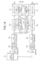
- Fig. 14 shows a block diagram of a circuit for improving input precision along the x- and y-axes.
- the circuit subtracts offset values from the input x-and y-coordinate signals and corrects the obtained signal.
- An x-coordinate offset value O xOFF for the detected x-coordinate O x is given by curve N in F ig. 12, and a y-coordinate offset value Q yOFF for the detected y-coordinate O y is given by curve M in Fig. 12.
- the correction circuit comprises x- and y-coordinate offset tables 53 x and 53y for storing offset values O xOFF and O yOFF , representing the difference between the input point and the nearest representative point, and subtracters 52 and 52 y for subtracting the offset values read out from the corresponding coordinate offset tables from the outputs of the A/D converters.
- Other arrangements of the circuit of Fig. 14 are substantially the same as those of Fig. 11.
- coordinate signals 0 0 (O x ,O y ) are generated by the input position detector 36, as is exemplified by the relationship between the coordinate signals and the coordinate correction coefficients of Fig. 12.
- the offset value O xOFF of the x-coordinate signal O x of the coordinate signals 0 0 (O x ,O y ) is stored at the address O y of the x-coordinate correction table 53 x .
- the offset value O yOFF of the y-coordinate signal O y of the coordinate signals 0 0 (O x ,O y ) is stored at the address O y of the y-coordinate correction table 53 .
- the following x-and y-coordinate correction coefficients C x and C y are stored at addresses (O x - O xOFF' O y - O yOFF ) of x - and y-coordinate tables 50 x and 50y:
- the coordinates I 0 (I x ,I y ) detected by the input position detector 36 are amplified by amplifiers 37 x and 37y to a predetermined level, and amplified outputs are sampled and held by sample-hold circuits 38 x and 38 . Outputs from the sample-hold circuits 38 and 38 y are then converted by A/D converters 39 x and 39 y to digital x- and y-coordinate signals.
- the digital x- and y-coordinate signals O x and O y are used as address signals to access the x- and y-coordinate offset tables 53 x and 53 .
- the x- and y-coordinate offset values O xOFF and O yOFF are subtracted by subtracters 52 x and 52y from the digital x- and y-coordinate signals O x and O y , respectively.
- the x- and y-coordinate correction tables 50 X and 50y are accessed in response to the differences (O x - O xOFF ) and (O y - O yOFF ) to read out the x- and y-coordinate correction coefficients:
- the product I x is generated as the corrected x-coordinate signal.
- the multiplier 51 y performs a multiplication of (O y - O yOFF ) x Cy, and produces the product I .
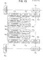
- Fig. 15 shows a coordinate input device with an obtaining circuit for obtaining coordinate correction coefficients of the input point by interpolating coordinate correction coefficients of a plurality of representative points according to still another embodiment of the present invention.
- Reference numerals 54 x to 56 x denote x-coordinate correction tables, respectively; 54 y to 56 , y-coordinate correction tables, respectively; 57 , 57 y , 60 x and 60 y , adders/subtracters, respectively; and 58 x , 58 , 59 x and 59 y , multipliers, respectively.
- Fig. 16 shows the principle of interpolation.
- the x-coordinate signal from the input position detector 36 is plotted along the abscissa, and the y-coordinate signal therefrom is plotted along the ordinate.
- Intersections between the dotted lines represent coordinates of the representative points with the preset coordinate correction coefficients.
- the coordinate correction coefficients can be calculated when an x-coordinate signal S x and a y-coordinate signal S y are generated by the input position detector 36.
- the x- and y-coordinate correction coefficients S cx and S cy are multiplied with the corresponding coordinate signals to correct the digital coordinate signals.
- the x-coordinate correction coefficient S cx in equation (1) is a correction coefficient of a representative point of the input surface of the input position detector 36 and is stored in the x-coordinate correction table 54 x in Fig. 15.
- the second term of represents an x-direction change in the x-coordinate correction coefficient S cx and-is stored in the x-coordinate correction table 55 x .
- (S x - O x1 ) is a difference between the x-coordinate position signal S x and the coordinate signal O x1 representing the readout correction coefficient. The is multiplied by the multiplier 58 x with the difference (S x - O x1 ).
- the third term is the same as the second term but represents y-coordinate components.
- a y - direction change of the x-coordinate correction coefficient S is stored in the cx x-coordinate correction table 56 x and is multiplied by the multiplier 59 x with the y-coordinate difference (S y - O y1 ).
- the first to third terms of equation (1) are added by the adders/subtracters 57 x and 60 x .
- a sum is multiplied by the multiplier 51 x with the x-coordinate signal S x , thereby correcting the x-coordinate signal S .
- the y-coordinate signal S can be corrected by the lower half of the circuit of Fig. 15 in accordance with equation (2).
- the coordinate correction coefficients stored in the coordinate correction tables can be multiplied to accurately detect the input point with high precision in the same manner as in the device of Fig. 11.
- the coordinate correction tables can be made reduced in volume.
- the coordinate correction coefficients are interpolated to further correct the coordinate detected values with higher precision.
- three x-coordinate correction tables and three y-coordinate correction tables are used in the above description.
- only one x-coordinate correction table and one y-coordinate correction table can be used together with adders and a microprocessor.
- the correction data stored in the input position correction tables are.coordinate correction coefficients of representative points on the input surface. These correction coefficients are multiplied with the detection signal to perform correction.
- the correction data may be differences between the coordinates of the input position on the input surface and the corresponding coordinates detected by the input position detector. In this case, the detected values are added and/or subtracted to perform correction.
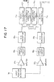
- Fig. 17 shows still another embodiment for implementing such correction.
- Reference numerals 70 x and 70y denote x-coordinate correction tables, respectively; and 71 and 71y, adders/subtracters, respectively.
- Other arrangements of the circuit of Fig. 17 are substantially the same as those of Fig. 11.
- x- and y-coordinate signals from an input position detector 36 are amplified by amplifiers 37 x and 37 y to a predetermined level, respectively.
- Amplified outputs are sampled and held by sample-hold circuits 38 x and 38 , respectively.
- Outputs from the sample-hold circuits 38 x and 38y are converted by A/D converters 39 x and 39 y from analog x-and y-coordinate signals to digital x- and y-coordinate signals.
- X- and y-coordinate correction differences corresponding to the x- and y-coordinate signals obtained by supplying the digital x- and y-coordinate signals as address signals to the x- and y-coordinate correction tables 70 x and 70 y , are added/subtracted by the adders/subtractors 71 x and 71y with the digital x-and y-coordinate signals, thereby obtaining the corrected x- and y-coordinate signals.
- Fig. 12 shows coordinate signals 0 0 (O x ,O y ) generated by the input position detector 36 upon detection of coordinates I 0 (I x ,I y ).
- x-and y-coordinate correction differences D and D y are given as follows:
- the coordinate detection error in the input position detector 36 of Fig. 17 is rarely subjected to steep changes, as shown in Fig. 12. Therefore, the coordinate correction differences need not be prepared for the entire surface of the input position detector 36.
- the coordinate correction differences can be prepared for several representative points of the input surface of the input position detector 36 and can be used to correct input points near the representative points.
- Fig. 18 is a circuit diagram for implementing the method described above according to still another embodiment of the present invention.
- An illustrated portion is a circuit different from the corresponding portion of the circuit of Fig. 17.
- the resolution of each of A/D converters 39 x and 39y is given as 10 bits.
- 10-bit data from the A/D converters 39 x and 39 y is supplied to multipliers 71 and 71 , respectively.
- the upper eight bits of each of the digital x- and y-coordinate data are supplied to corresponding x- and y-coordinate correction tables 70 and 70 .
- the number of bits constituting the data supplied to the x- and y-coordinate correction tables 70 x and 70y can be decreased. For this reason, the number of x-coordinate correction differences stored in the x-coordinate correction table 70 is 2 16 , 1/16 when the correction differences for all input points are prepared.
- the x- and y-coordinate correction differences stored in the x- and y-coordinate correction tables 70 x and 70 y are added to or subtracted from the output, thereby detecting the input position with high precision.
- Fig. 19 shows a coordinate input device with an interpolation circuit for obtaining coordinate correction differences of the input point by interpolating coordinate correction differences of a plurality of representative points according to still another embodiment of the present invention.
- Reference numerals 72 to 74 denote x-coordinate correction x x tables, respectively; 72 y to 74 y , y-coordinate correction tables, respectively; 75 x , 75 y , 78 x and 78 , adders/subtracters, respectively; and 76 x , 76 y , 77 x and 77 y , multipliers, respectively.
- the principle of interpolation is substantially the same as that in the embodiment of Fig. 15 described with reference to Fig. Fig. 16.
- the x-coordinate signal from the input position detector 36 is plotted along the abscissa, and the y-coordinate signal therefrom is plotted along the ordinate. Intersections between the dotted lines represent-coordinates of the representative points with the preset coordinate correction differences.
- the coordinate correction differences can be calculated when an x-coordinate signal S x and a y-coordinate signal S y are generated by the input position detector 36. It should be noted that the coefficients C are replaced with the differences D in this embodiment.
- the x- and y-coordinate correction differences S dx and S d y are multiplied with the corresponding coordinate signals to correct the digital coordinate signals.
- the x-coordinate correction differences S dx in equation (3) are considered.
- the first term D 11x is a correction difference of a representative point of the input surface of the input position detector 36 and is stored in the x-coordinate correction table 72 in x F ig. 19 .
- the second term of (D 12x - D 11x )/(O x2 - O x1 ) represents an x-direction change in the x-coordinate correction difference S dx and is stored in the x-coordinate correction table 73 x .
- (S - O x1 ) is a difference between the x-coordinate position signal S x and the coordinate signal O x1 representing the readout correction difference.
- a sum is added by the adder/subtracter 71 to the x-coordinate signal S , thereby correcting the x-coordinate signal S .
- the y-coordinate signal S can be corrected by the lower half of the circuit of Fig. 19 in accordance with equation (4).
- the coordinate correction differences stored in the coordinate correction tables can be subjected to addition/subtraction to accurately detect the input point with high precision in the same manner as in the device of Fig. 17.
- the coordinate correction tables can be reduced in volume.
- the coordinate correction differences are interpolated to further correct the coordinate detected values with higher precision.
- three x-coordinate correction tables and three y-coordinate correction tables are used in the above description.
- only one x-coordinate correction table and one y-coordinate correction table can be used together with adders and a microprocessor.
- the coordinate correction difference data of the representative points of the input surface are stored in correspondence with the input position detection errors inherent to the input position detector.
- the coordinate correction difference data or the values obtained by interpolating the coordinate correction difference data are added to or subtracted from the coordinate signal. Therefore, the coordinate correction tables can be reduced in volume, and high-precision coordinate detection can be performed. Furthermore, even if the input position detector has a detection error, it can be used as the detector, thereby increasing the yield of the products at low cost.
- a coordinate input device as a coordinate input/display device having a transparent coordinate input unit (i.e., a transparent drawing pad) and a coordinate display unit integrally arranged with the the transparent coordinate input unit so as to match an coordinate input point with a coordinate display point will be described according to still another embodiment of the present invention.
- a transparent coordinate input unit i.e., a transparent drawing pad
- a coordinate display unit integrally arranged with the the transparent coordinate input unit so as to match an coordinate input point with a coordinate display point
- Fig. 20 is a block diagram of the coordinate input/display device.
- reference numeral 81 denotes a coordinate input unit of the coordinate input/display device; 82 and 82 , amplifiers, respectively; 83 and 83 , sample-hold circuits, respectively; 84 and 84 , A/D converters, respectively; 85 and 85y, subtracters, respectively; 86 and 86 , x- and y-coordinate correction tables constituted by programable random-access memories (PRAMs), respectively; 87 x and 87 y , adders/subtracters; 88, a coordinate display unit of the coordinate input/display unit; and 89, a video memory for the coordinate display unit 18.
- PRAMs programable random-access memories
- Reference numeral 90 denotes a video memory control circuit; 91 , an x-coordinate generator; and 91 , a y-coordinate generator.
- the video memory control circuit 90, the x-and y-coordinate generators 91 and 92 constitute a display circuit.
- Reference numeral 92 denotes an operation mode control circuit.
- the coordinate input unit 81 and the coordinate display unit 88 shown in Fig. 20 are integrally formed as shown in Fig. 21.
- the coordinate input unit 81 and the coordinate display unit 88 are separately illustrated in Fig. 20 for illustrative convenience.
- the coordinate display unit 88 can comprise a flat display such as a liquid crystal display panel or a plasma display panel.
- the coordinate display unit 88 are operated by the operation mode control circuit 92 in one of the two operating modes (i.e., the coordinate input/display mode and the coordinate correction difference write mode).
- x- and y-coordinate correction differences D and D y are prestored in the x- and y-coordinate correction tables 86 and 86 , respectively.
- the operation mode control circuit 92 is operated in the coordinate input/display mode, that the x- and y-coordinate correction tables 86 x and 86y are set by the operation mode control circuit 92 in the read mode, and that the video memory control circuit 90 selects coordinate data from the adders/subtracters 87 and 87 .
- X- and y-coordinate signals from the coordinate input unit 81 are amplified by the amplifiers 82 x and 82 y to a predetermined level, respectively.
- Amplified outputs are sampled and held by the sample-hold circuits 83 x and 83 , respectively.
- Analog outputs from the sample-hold circuits 83 x and 83y are converted by the A/D converters 84 x and 84 to digital x- and y-coordinate signals.
- the digital x-and y-coordinate signals are supplied to the x- and y-coordinate correction tables 86 x and 86 for storing coordinate correction differences determined by the characteristics of the coordinate input unit 81.
- the x- and y-coordinate correction differences corresponding to the input data are added to or subtracted from the digital x- and y-coordinate position signals by the adders/subtracters 87 x and 87 , thereby generating the corrected x- and y-coordinate signals.
- the corrected x- and y-coordinate signals from the adders/subtractors 87 x and 87y are selected by the video memory control circuit 90 and are selectively written in the video memory 89, thereby displaying the coordinate data on the coordinate display unit 88.
- the x- and y-coordinate correction values stored in the x- and y-coordinate correction tables 86 comprise the differences D and D .
- the correction technique is the same as that described in the embodiment of Fig. 17, and a detailed description thereof will be omitted.
- the coordinate correction value write mode of the circuit shown in Fig. 20 will be described hereinafter.
- the operation mode control circuit 92 sets the x- and y-coordinate correction tables 86 x and 86y in the coordinate correction value write mode, the x- and y-coordinate generators 91 X and 91 y in an active state, and the video memory control circuit 90 in a mode to select the coordinate data from the x- and y-coordinate generators 91 x and 91y.
- One point is displayed by the x- and y-coordinate generators 91 x and 91y on the coordinate display unit 88.
- Three points corresponding to the display screen of the coordinate display unit 88 are entered from the coordinate input unit 81.
- Fig. 22 shows the relationship between the coordinate input points and display outputs as the coordinate signals in response to the coordinate inputs.
- Reference numeral 93 denotes input coordinates; and 94, coordinate detected values. More specifically, when coordinates for points A, B, C, and D of Fig. 22 are sequentially generated by the x- and y-coordinate generators 91 x and 91y of Fig. 20, the corresponding dots on the coordinate display unit 88 are accordingly 'turned on, thereby registering the coordinates of points corresponding to the input points on the coordinate input unit 81.
- x- and y-coordinate signals 0 and 0 are generated by the coordinate input unit 81.
- digital x- and y-coordinate signals O x and O y converted by the A/D converters 84 x and 84y are generated.
- the x-coordinate signal O x is subtracted by the subtracter 85 x from the digital x-coordinate signal Ix generated by the x-coordinate generator 91 to produce the difference (I x - O x ).
- the difference (I x - O x ) is written as x-coordinate correction value at the address (O x ,O y ) of the x-coordinate table 86 .
- the y-coordinate signal O y is subtracted from the digital coordinate signal I y generated by the y-coordinate generator 91 to obtain a difference (I - O y ).
- the difference (I - O y ) is stored at the address (O x ,O y ).
- the above operation is repeated for the coordinates of the representative points in the coordinate input unit 81, thereby preparing the x- and y-coordinate correction tables 86 and 86 .
- the coordinate detection error can be corrected by the coordinate correction differences stored in the x- and y-coordinate correction tables 86 x and 86 . Therefore, the input coordinates 93 can be detected with high precision.
- the correction is performed, so that the coordinate input point matches with the display point, thereby allowing effective entering of coordinate data and decreasing the adjustment cost.
- the two sample-hold circuits 83 x and 83 y and the two A/D converters circuits 84 x and 84 y are used for illustrative convenience. However, when the x- and y-coordinate signals are time-divisionally driven, only one sample-hold circuit and one A/D converter are required. Furthermore, even if the coordinate display unit 18 has a unit such as a CRT with a peripheral display distortion, errors of the coordinate input unit 81 and the coordinate display unit 88 can be corrected by the x- and y-coordinate generators as a whole.
- a portion of the correction circuit constituted by the x- and y-coordinate correction tables 86 x and 86y is arranged in the same manner as in the correction circuit of Fig. 19.
- the same effect as in the device of Fig. 19 can be obtained in the device of Fig. 20.
- the coordinate correction data stored in the coordinate correction tables in the device of Fig. 20 is exemplified by difference data.
- the coordinate correction coefficients can be used in place of the difference data.
- the x- and y-coordinate correction tables 86 x and 86y of Fig. 20 are replaced with the x- and y-coordinate correction tables 50 x and 50y in Fig. 11; the adders/subtracters 87 and 87 , with the multipliers 51 and 51 ; and the subtracters 85 and 85 , with dividers.
- a high-precision transparent drawing pad overlaps a flat display panel such as a liquid crystal display panel or a plasma display panel.
- An input character or graphic pattern can be checked on the flat display.
- the input position of the transparent drawing pad matches with the display position on the flat display irrespective of the input conditions of the electrical pen. Therefore, the operator can easily add or erase character and graphic patterns, resulting in convenience.
- the coordinate signals generated by the coordinate generators and the coordinate input unit are displayed on the coordinate display unit.
- the coordinate signals corresponding to the displayed points are generated by the coordinate input unit upon registration of the coordinates representing the displayed points and are calculated to derive a coordinate correction value which is then stored in the coordinate correction table.
- the coordinate input/display device uses the coordinate correction value to correct a coordinate signal from the coordinate input unit.
- the coordinate input point thus matches with the the displayed point, and the coordinate input operation is easy.
- high-precision coordinate position detection can be performed. Even if the coordinate input unit and the coordinate position detector are subjected deterioration over time, the coordinate correction tables can be easily updated.
- a DC voltage is applied across the transparent resistor film to detect the coordinates.
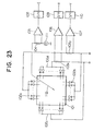
- an AC voltage may be used to detect the coordinates, as exemplified in Figs. 23 and 24.
- Fig. 23 is a block diagram of a coordinate input device driven with an AC voltage
- Fig. 24 is a timing chart for explaining the operation thereof.
- x-coordinate detection electrodes 102c and 102d in a transparent input panel 101 are arranged along the current flow-in direction, and y-coordinate detection electrodes 102a and 102b are arranged along the current flow-out direction.
- An AC power source (a rectangular wave power source) 111 is connected to an electrical pen 112 through a detection resistor 104. Both ends of the detection resistor 104 are connected to inputs of an operational amplifier 105, and the output thereof is connected to the input of a sample-hold circuit 108.
- the detection electrodes 102b and 102c are grounded.
- Detection resistors 103 X and 103 are connected between the detection electrode 102a and ground and between the detection electrode 102d and ground, respectively.
- Both ends of the detection resistors 103 and 103 are connected to the x y inputs of operational amplifiers 106 and 107.
- the outputs of the operational amplifiers 106 and 107 are connected to the inputs of sample-hold circuits 109 and 110, respectively.
- a rectangular wave signal with an amplitude of +E (Fig. 24) is supplied from the AC power source 111 to the transparent resistor film through the electrical pen 112
- rectangular wave currents with amplitudes of -i x and i y flow through the detection resistors 103 and 103 , respectively.
- Rectangular wave currents with amplitudes of -i and +iy flow through the detection resistor 104.
- the x-and y-coordinates can be given by these currents:
- the outputs E and X are proportional to the currents i ex and i x during the negative period of the voltage
- the outputs E and Y are proportional to the currents i ey and i y during the positive period of the voltage. Therefore, the currents i x and i y are divided by the currents i ex and i ey to detect the x and y coordinates, respectively.
Landscapes
- Engineering & Computer Science (AREA)
- General Engineering & Computer Science (AREA)
- Theoretical Computer Science (AREA)
- Human Computer Interaction (AREA)
- Physics & Mathematics (AREA)
- General Physics & Mathematics (AREA)
- Position Input By Displaying (AREA)
Applications Claiming Priority (16)
| Application Number | Priority Date | Filing Date | Title |
|---|---|---|---|
| JP59241921A JPS61120230A (ja) | 1984-11-16 | 1984-11-16 | 位置入力装置 |
| JP241921/84 | 1984-11-16 | ||
| JP59262965A JPS61141025A (ja) | 1984-12-14 | 1984-12-14 | 座標検出装置 |
| JP262965/84 | 1984-12-14 | ||
| JP2454/85 | 1985-01-10 | ||
| JP60002454A JPS61161535A (ja) | 1985-01-10 | 1985-01-10 | 透明形座標入力装置用入力面 |
| JP23547/85 | 1985-02-12 | ||
| JP23548/85 | 1985-02-12 | ||
| JP60023548A JPS61183733A (ja) | 1985-02-12 | 1985-02-12 | 入力位置検出装置の入力位置補正方法 |
| JP60023547A JPS61183732A (ja) | 1985-02-12 | 1985-02-12 | 入力位置検出装置の入力位置補正方法 |
| JP33695/85 | 1985-02-23 | ||
| JP60033695A JPS61194523A (ja) | 1985-02-23 | 1985-02-23 | 座標入力表示装置 |
| JP216203/85 | 1985-10-01 | ||
| JP60216203A JPS6277626A (ja) | 1985-10-01 | 1985-10-01 | 座標入力装置用透明入力面 |
| JP60234588A JPS6295626A (ja) | 1985-10-22 | 1985-10-22 | 座標入力表示装置 |
| JP234588/85 | 1985-10-22 |
Publications (3)
| Publication Number | Publication Date |
|---|---|
| EP0182715A2 true EP0182715A2 (fr) | 1986-05-28 |
| EP0182715A3 EP0182715A3 (en) | 1988-08-10 |
| EP0182715B1 EP0182715B1 (fr) | 1992-03-18 |
Family
ID=27571463
Family Applications (1)
| Application Number | Title | Priority Date | Filing Date |
|---|---|---|---|
| EP19850402221 Expired EP0182715B1 (fr) | 1984-11-16 | 1985-11-15 | Appareil d'entrée de coordonnées |
Country Status (2)
| Country | Link |
|---|---|
| EP (1) | EP0182715B1 (fr) |
| DE (1) | DE3585665D1 (fr) |
Cited By (5)
| Publication number | Priority date | Publication date | Assignee | Title |
|---|---|---|---|---|
| EP0230202A3 (fr) * | 1985-10-25 | 1989-08-30 | Scriptel Corporation | Système et méthode électrographiques d'entrée de coordonnées |
| FR2688082A1 (fr) * | 1992-02-27 | 1993-09-03 | Gunze Kk | Dispositif a panneau tactile. |
| FR2728708A1 (fr) * | 1994-12-26 | 1996-06-28 | Samsung Display Devices Co Ltd | Dispositif d'identification d'une coordonnee de position et procede d'identification mis en oeuvre dans ce dispositif |
| EP0782091A1 (fr) * | 1995-12-21 | 1997-07-02 | Siemens-Elema AB | Panneau avant d'un appareil |
| CN101587413B (zh) * | 2008-05-19 | 2011-07-20 | 富士通电子零件有限公司 | 制造坐标检测器的方法 |
Family Cites Families (1)
| Publication number | Priority date | Publication date | Assignee | Title |
|---|---|---|---|---|
| GB1280341A (en) * | 1969-03-13 | 1972-07-05 | Automatic Radio Mfg Co | Improvements in and relating to position responsive apparatus |
-
1985
- 1985-11-15 DE DE8585402221T patent/DE3585665D1/de not_active Expired - Lifetime
- 1985-11-15 EP EP19850402221 patent/EP0182715B1/fr not_active Expired
Cited By (6)
| Publication number | Priority date | Publication date | Assignee | Title |
|---|---|---|---|---|
| EP0230202A3 (fr) * | 1985-10-25 | 1989-08-30 | Scriptel Corporation | Système et méthode électrographiques d'entrée de coordonnées |
| FR2688082A1 (fr) * | 1992-02-27 | 1993-09-03 | Gunze Kk | Dispositif a panneau tactile. |
| FR2728708A1 (fr) * | 1994-12-26 | 1996-06-28 | Samsung Display Devices Co Ltd | Dispositif d'identification d'une coordonnee de position et procede d'identification mis en oeuvre dans ce dispositif |
| EP0782091A1 (fr) * | 1995-12-21 | 1997-07-02 | Siemens-Elema AB | Panneau avant d'un appareil |
| US5859631A (en) * | 1995-12-21 | 1999-01-12 | Siemens Elema Ab | Apparatus front panel allowing indicia on an indicia-bearing element to be read therethrough |
| CN101587413B (zh) * | 2008-05-19 | 2011-07-20 | 富士通电子零件有限公司 | 制造坐标检测器的方法 |
Also Published As
| Publication number | Publication date |
|---|---|
| EP0182715B1 (fr) | 1992-03-18 |
| DE3585665D1 (de) | 1992-04-23 |
| EP0182715A3 (en) | 1988-08-10 |
Similar Documents
| Publication | Publication Date | Title |
|---|---|---|
| US4752655A (en) | Coordinate input device | |
| US4788384A (en) | Device for two-dimensional localization of events that generate current on a resistive surface | |
| US5198623A (en) | Method for use in a digitizer for determining pen tilt | |
| US6081259A (en) | Method and apparatus for reducing noise in an electrostatic digitizer | |
| US5886687A (en) | Touch panel system utilizing capacitively-coupled electrodes | |
| US5796389A (en) | Reduced noise touch screen apparatus and method | |
| JP2934506B2 (ja) | 透明な導電性グリッドを有する透視形ディジタイザ | |
| EP0565300B1 (fr) | Méthode pour la correction de position de lieu d'indicateur pour un système d'affichage | |
| EP1656608B1 (fr) | Element d'ecran tactile anisotrope | |
| US5790106A (en) | Coordinate input apparatus with pen and finger input detection | |
| JP3278117B2 (ja) | タッチセンサーパネル用のアルゴリズム補正システムおよびその方法 | |
| US9569053B2 (en) | Wide dynamic range capacitive sensing | |
| US7920134B2 (en) | Periodic sensor autocalibration and emulation by varying stimulus level | |
| JP3121592B2 (ja) | 液晶表示装置 | |
| JPH061429B2 (ja) | タッチパネル・システムの位置測定装置 | |
| JPS59189437A (ja) | 空間座標を検出するための改良形システム | |
| US6366866B1 (en) | Coordinates detecting apparatus for independently correcting coordinates | |
| US5777898A (en) | Method and apparatus for aligning a digitizing panel with a display device | |
| EP0182715B1 (fr) | Appareil d'entrée de coordonnées | |
| US4798920A (en) | Stylus coordinate determining device with distortion compensation | |
| JP5768386B2 (ja) | 座標入力システム | |
| EP0203188A1 (fr) | Methode et dispositif de localisation electronique d'un point de touche | |
| JPH05324164A (ja) | 位置検出装置 | |
| EP0942390B1 (fr) | Ecran tactile résistif | |
| JP4125862B2 (ja) | タッチパネル装置 |
Legal Events
| Date | Code | Title | Description |
|---|---|---|---|
| PUAI | Public reference made under article 153(3) epc to a published international application that has entered the european phase |
Free format text: ORIGINAL CODE: 0009012 |
|
| AK | Designated contracting states |
Kind code of ref document: A2 Designated state(s): DE FR GB |
|
| PUAL | Search report despatched |
Free format text: ORIGINAL CODE: 0009013 |
|
| AK | Designated contracting states |
Kind code of ref document: A3 Designated state(s): DE FR GB |
|
| 17P | Request for examination filed |
Effective date: 19881114 |
|
| 17Q | First examination report despatched |
Effective date: 19900510 |
|
| GRAA | (expected) grant |
Free format text: ORIGINAL CODE: 0009210 |
|
| AK | Designated contracting states |
Kind code of ref document: B1 Designated state(s): DE FR GB |
|
| REF | Corresponds to: |
Ref document number: 3585665 Country of ref document: DE Date of ref document: 19920423 |
|
| ET | Fr: translation filed | ||
| PLBE | No opposition filed within time limit |
Free format text: ORIGINAL CODE: 0009261 |
|
| STAA | Information on the status of an ep patent application or granted ep patent |
Free format text: STATUS: NO OPPOSITION FILED WITHIN TIME LIMIT |
|
| 26N | No opposition filed | ||
| PGFP | Annual fee paid to national office [announced via postgrant information from national office to epo] |
Ref country code: GB Payment date: 19951106 Year of fee payment: 11 |
|
| PGFP | Annual fee paid to national office [announced via postgrant information from national office to epo] |
Ref country code: DE Payment date: 19951113 Year of fee payment: 11 |
|
| PGFP | Annual fee paid to national office [announced via postgrant information from national office to epo] |
Ref country code: FR Payment date: 19951130 Year of fee payment: 11 |
|
| REG | Reference to a national code |
Ref country code: FR Ref legal event code: CA |
|
| PG25 | Lapsed in a contracting state [announced via postgrant information from national office to epo] |
Ref country code: GB Effective date: 19961115 |
|
| GBPC | Gb: european patent ceased through non-payment of renewal fee |
Effective date: 19961115 |
|
| PG25 | Lapsed in a contracting state [announced via postgrant information from national office to epo] |
Ref country code: FR Effective date: 19970731 |
|
| PG25 | Lapsed in a contracting state [announced via postgrant information from national office to epo] |
Ref country code: DE Effective date: 19970801 |
|
| REG | Reference to a national code |
Ref country code: FR Ref legal event code: ST |