EP0182717A2 - Circuit de mémoire morte - Google Patents
Circuit de mémoire morte Download PDFInfo
- Publication number
- EP0182717A2 EP0182717A2 EP85402244A EP85402244A EP0182717A2 EP 0182717 A2 EP0182717 A2 EP 0182717A2 EP 85402244 A EP85402244 A EP 85402244A EP 85402244 A EP85402244 A EP 85402244A EP 0182717 A2 EP0182717 A2 EP 0182717A2
- Authority
- EP
- European Patent Office
- Prior art keywords
- transistor
- circuit
- gate
- rom
- memory
- Prior art date
- Legal status (The legal status is an assumption and is not a legal conclusion. Google has not performed a legal analysis and makes no representation as to the accuracy of the status listed.)
- Granted
Links
Images

Classifications
-
- G—PHYSICS
- G11—INFORMATION STORAGE
- G11C—STATIC STORES
- G11C16/00—Erasable programmable read-only memories
- G11C16/02—Erasable programmable read-only memories electrically programmable
- G11C16/04—Erasable programmable read-only memories electrically programmable using variable threshold transistors, e.g. FAMOS
- G11C16/0408—Erasable programmable read-only memories electrically programmable using variable threshold transistors, e.g. FAMOS comprising cells containing floating gate transistors
- G11C16/0441—Erasable programmable read-only memories electrically programmable using variable threshold transistors, e.g. FAMOS comprising cells containing floating gate transistors comprising cells containing multiple floating gate devices, e.g. separate read-and-write FAMOS transistors with connected floating gates
Definitions
- the present invention relates to a semiconductor integrated circuit, more specifically to a read only memory circuit suitable to be incorporated in an integrated circuit.
- one or more redundant circuit blocks are provided for semiconductor integrated circuits, particularly for semiconductor memory devices.
- the redundant circuit blocks are usually formed in advance on a semiconductor chip to constitute an integrated circuit network with other circuit blocks. If a faulty circuit, a memory cell, for example, is found during the test performed on the fabricated integrated circuit, the faulty circuit is replaced by a redundant circuit having equivalent specialized functions, and thus, the desired comprehensive functions of the integrated circuit can be insured on the chip.
- a circuit having a fuse with which the circuit generates control signals to inform of the use of the redundant circuit blocks according to ON or OFF state of the fuse is also provided.
- FIG. 4 is an equivalent circuit diagram showing an exemplary conventional control signal generating circuit, a kind of read only memory (RO M ), comprising a fuse.
- a fuse 51 is made OFF by supplying an input signal B to the gate of an n-channel transistor 52.
- Reference 53 designates a resistor.
- One end of the fuse 51 is connected to a voltage source Vcc (+5 volts, for example) and another end of the fuse is connected to a node of a resistor 53 and the drain of the transistor 52.
- the control signals (output signals) C are provided from the node.
- the fuse 51 is made to remain ON, the voltage at the node is substantially equal to Vcc and control signals C of high level are output, whereas when the fuse 51 has been made OFF, the node voltage, i. e. the control signal level becomes low.
- the OFF state of the fuse is realized as follows:
- a faulty circuit in a semiconductor integrated circuit is described by taking a faulty memory on a memory chip as an example. If a faulty memory cell is detected during the chip test process, the fuses are made OFF or remain as ON so as to produce a binary information consisting of high level (1) and/or low level (0) signals, corresponding to the respective addresses of the row and column relevant to the faulty cell. In the circuit of FIG.4, a low level signal (0) is output if the fuse 51 is made OFF, as mentioned above.
- the address input to the memory chip are compared with the information comprising the high and/or low level signals corresponding to the state of the fuses, and if a correspondence between the addresses and the information is detected, the row or column relevant to the faulty cell is operatively disconnected from the memory circuit and the redundant circuit block is connected instead. Thus, a faulty circuit containing the faulty memory cell is replaced by the redundant circuit block.
- one or more fuses are used in the ROM for informing of the use of the redundant circuit block in a conventional semiconductor integrated circuit.
- the incoming address signals are compared with the combination of the ON or OFF states of the fuses and a judgement whether they correspond to the address signals corresponding to the faulty circuit or not is carried out. If the correspondence between the incoming address signals and the addresses of the faulty circuit is detected, the redundant circuit block is instructed to substitute for the faulty circuit.
- Such destructive techniques as the blow-up of the fuse provides another kind of disadvantage such as producing cracks in the cover layer, usually a glass layer formed on the surface of a semiconductor chip for the passivation purposes, and remains in the cause of the failure in a semiconductor integrated circuit formed thereunder due to the adsorption of moisture which penetrates through the cracks and gives deleterious influences to the circuit. Accordingly, the reliability of the ROM comprising the fuses is insufficient for high quality integrated circuits, in general.
- the primary object of the present invention to provide a high reliability ROM circuit.
- ROM circuit to be incorporated in an integrated circuit for producing control signals to inform of the use of a redundancy circuit.
- a ROM circuit comprising terminal means for receiving a predefined input signal, a first transistor, a depletion type second transistor and a first and a second resistive means, wherein the first transistor has a channel region, a control gate formed so as to face the channel region and connected to the terminal means, a floating gate formed between the control gate and the channel region, and a source or drain, and the second transistor has a gate, which is connected to the floating gate of the first transistor, and a source or drain. Further, the first resistive means is connected between the control gate and the source or drain of the first transistor, and the second resistive means is connected between the source or drain of the second transistor and a voltage source.
- control gate When the control gate is provided with the predefined input signal applied to the terminal means, information corresponding to the input signal is stored on the floating gate, and the second transistor operatively outputs a high or low signal from the node of its source or drain and said second resistive means according to the predetermined input signal.
- the control gate of a first transistor when an input signal of a predefined high voltage is provided to the control gate of a first transistor, negative charges (electrons) are accumulated on the floating gate thereof, and the second transistor turns off due to the negative potential on the gate thereof, which is connected to the floating gate.
- the input signal when the input signal is not applied to the control gate of the first transistor, such accumulation of electrons on the floating gate does not occur, and hence, the second transistor maintains its conduction.
- the second transistor takes either a turned-on or turned-off state according to the existence of electrons accumulated on the floating gate, and a control signal corresponding to the on or off state is provided from the second transistor.
- the control signal can be used for informing of whether a faulty circuit, a memory circuit containing a faulty memory cell, for example, is replaced by a redundant circuit as explained before.
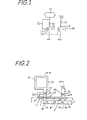
- FIG. 1 is an equivalent diagram showing a ROM circuit for generating a control signal in accordance with the aforesaid objects of the present invention.
- a first transistor 1 which is an n-channel transistor, comprises a control gate 11 and a floating gate 12 formed to face the control gate 11.
- a predefined voltage input signal is supplied to the control gate 11 via a terminal means 31 such as a pad and a wiring line 32 of aluminium, for example.
- the arrangement of the control gate 11 and the floating gate 12 will be shown later with reference to the plan view of FIG.2 and the cross-sectional views of FIGS 3A-3C.
- the gate of the second transistor 2 is kept at 0 potential. Accordingly, the second transistor 2 selected to be of the depletion type as mentioned before is not turned off in this case, and the control signal A of low level is output.
- the ROM circuit of the present invention as shown in FIG. 1 can avoid so-called soft write in the conventional ROMs having a floating gate, though comprising the first transistor 1 which is basically the same as well known SAMOS (stacked gate avalanche injection MOS).
- SAMOS stacked gate avalanche injection MOS
- the above- mentioned electron injection may occur statistically with the application of relatively lower voltage such as a few volts.
- This is the soft write occurring during read mode and causes an erroneous write into a ROM whose floating gate has not been provided with the carrier injection during write mode.
- source-drain voltage must be restricted as low as 1 volt or less, for example, in the read mode and complex circuits for the read-out and level conversion are required for the conventional ROMs.
- the soft write is avoided.
- the read out of the information stored in the first transistor 1 is carried out by the second transistor 2. Being selected to be of the depletion type, the second transistor 2 is turned off by the negative potential on the floating gate 12 of the first transistor and outputs a high level signal, while keeping its conduction to provide a low level signal if the floating gate 12 has not been provided with electron accumulation thereon.
- control signal generating circuit of the present invention uses information whether electrons are accumulated on the floating gate 12 of the first transistor 1 or not for determining the use of a redundant circuit, instead of the conventional means depending on the ON or OFF states of the fuses and, therefore, it can provide high reliability control signals.
- the circuit of the present invention is simple not requiring complex read-out and level conversion circuits and is suitable to be incorporated in an integrated circuit on a chip.
- the reliability is equal to that achieved by using conventional EPROM (erasable programmable ROM) cells.
- EPROM erasable programmable ROM
- the structure of an existing EPROM cell can be employed for the first transistor in the present invention.
- the electrons accumulated on the floating gate of a selected first transistor must be persistent so long as the circuit is used. Therefore, the erasable function by an ultraviolet (UV) light in an EPROM is not necessary for the circuit, and an OTPROM (one time PROM) equipped with no window for the UV exposure is suitable to the substitution for the first transistor in the present invention.
- UV ultraviolet
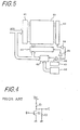
- FIG. 5 is a circuit block diagram showing a conceptual configuration of a semiconductor memory circuit including a redundant circuit and a control signal generating circuit comprising the ROM circuits of the present invention.
- the access to a memory cell in a memory cell matrix 60 is carried out according to the address data ADD input to a column address decoder 61 and a row address decoder 62 as in the conventional memory circuits.
- a redundant circuit 63 corresponding to a memory cell row in the matrix 60. If a faulty memory cell is detected during a test process, information relevant to the column address and row address of the faulty cell is stored in an auxiliary memory block 64 comprising the ROM circuits, each of which has the circuit configuration as shown in FIG.1.
- the incoming address data to the decoder 61 and 62 are compared with the information stored in the auxiliary memory block 64 by means of a comparator 65, and if correspondence between the incoming address and the information is detected, the comparator 65 outputs a control signal for making the row address decoder inactive while activating the redundant circuit 63.
- the comparator 65 outputs a control signal for making the row address decoder inactive while activating the redundant circuit 63.
- the output signal of the comparator 65 is checked by the gate 66 which outputs an effective control signal according to the fault information stored in another auxiliary memory 67 comprising a ROM circuit as shown in FIG.1.
- reference 68 designates a driver for actuating the redundant circuit 63
- reference 69 designates an inverter which operates to activate the row address decoder 62 only when the output control signal from the comparator 65 is in a low level.
Landscapes
- Engineering & Computer Science (AREA)
- Microelectronics & Electronic Packaging (AREA)
- Non-Volatile Memory (AREA)
- Read Only Memory (AREA)
- Semiconductor Memories (AREA)
- For Increasing The Reliability Of Semiconductor Memories (AREA)
- Design And Manufacture Of Integrated Circuits (AREA)
Applications Claiming Priority (2)
| Application Number | Priority Date | Filing Date | Title |
|---|---|---|---|
| JP59243326A JPS61123169A (ja) | 1984-11-20 | 1984-11-20 | 半導体集積回路 |
| JP243326/84 | 1984-11-20 |
Publications (3)
| Publication Number | Publication Date |
|---|---|
| EP0182717A2 true EP0182717A2 (fr) | 1986-05-28 |
| EP0182717A3 EP0182717A3 (en) | 1988-04-27 |
| EP0182717B1 EP0182717B1 (fr) | 1991-01-30 |
Family
ID=17102162
Family Applications (1)
| Application Number | Title | Priority Date | Filing Date |
|---|---|---|---|
| EP85402244A Expired - Lifetime EP0182717B1 (fr) | 1984-11-20 | 1985-11-20 | Circuit de mémoire morte |
Country Status (5)
| Country | Link |
|---|---|
| US (1) | US4725980A (fr) |
| EP (1) | EP0182717B1 (fr) |
| JP (1) | JPS61123169A (fr) |
| KR (1) | KR900000586B1 (fr) |
| DE (1) | DE3581596D1 (fr) |
Families Citing this family (15)
| Publication number | Priority date | Publication date | Assignee | Title |
|---|---|---|---|---|
| JPS63252481A (ja) * | 1987-04-09 | 1988-10-19 | Toshiba Corp | 不揮発性半導体メモリ |
| US4870304A (en) * | 1987-12-08 | 1989-09-26 | Cypress Semiconductor Corporation | Fast EPROM programmable logic array cell |
| DE68928112T2 (de) * | 1988-03-18 | 1997-11-20 | Toshiba Kawasaki Kk | Masken-rom mit Ersatzspeicherzellen |
| JPH0249463A (ja) * | 1988-05-27 | 1990-02-19 | Matsushita Electron Corp | 半導体装置 |
| JPH07120726B2 (ja) * | 1990-05-30 | 1995-12-20 | 株式会社東芝 | 不揮発性半導体メモリ |
| US5132933A (en) * | 1990-12-21 | 1992-07-21 | Schreck John F | Bias circuitry for nonvolatile memory array |
| JP2829156B2 (ja) * | 1991-07-25 | 1998-11-25 | 株式会社東芝 | 不揮発性半導体記憶装置の冗長回路 |
| FR2697673B1 (fr) * | 1992-10-29 | 1994-12-16 | Gemplus Card Int | Circuit à fusible, pour circuit intégré. |
| WO1996015553A1 (fr) * | 1994-11-15 | 1996-05-23 | Advanced Micro Devices, Inc. | Structure de transistor possedant des surfaces de grille et de pastille speciales |
| US6031771A (en) * | 1996-10-28 | 2000-02-29 | Macronix International Co., Ltd. | Memory redundancy circuit using single polysilicon floating gate transistors as redundancy elements |
| JPH11189883A (ja) * | 1997-10-20 | 1999-07-13 | Alps Electric Co Ltd | 修復された金属パターンを有する基板および基板上の金属パターン修復方法と修復装置 |
| US5896327A (en) * | 1997-10-27 | 1999-04-20 | Macronix International Co., Ltd. | Memory redundancy circuit for high density memory with extra row and column for failed address storage |
| US5889711A (en) * | 1997-10-27 | 1999-03-30 | Macronix International Co., Ltd. | Memory redundancy for high density memory |
| US6049495A (en) * | 1999-02-03 | 2000-04-11 | International Business Machines Corporation | Auto-programmable current limiter to control current leakage due to bitline to wordline short |
| US8058469B2 (en) * | 2008-11-03 | 2011-11-15 | Sabic Innovative Plastics Ip B.V. | Method for making carbamates, ureas and isocyanates |
Family Cites Families (8)
| Publication number | Priority date | Publication date | Assignee | Title |
|---|---|---|---|---|
| US4305083A (en) * | 1978-09-19 | 1981-12-08 | Texas Instruments Incorporated | Single junction charge injector floating gate memory cell |
| US4245165A (en) * | 1978-11-29 | 1981-01-13 | International Business Machines Corporation | Reversible electrically variable active parameter trimming apparatus utilizing floating gate as control |
| US4375087C1 (en) * | 1980-04-09 | 2002-01-01 | Hughes Aircraft Co | Electrically erasable programmable read-only memory |
| US4348745A (en) * | 1980-10-27 | 1982-09-07 | Hughes Aircraft Company | Non-volatile random access memory having non-inverted storage |
| US4573144A (en) * | 1982-09-30 | 1986-02-25 | Motorola, Inc. | Common floating gate programmable link |
| US4532611A (en) * | 1982-11-01 | 1985-07-30 | Motorola, Inc. | Redundant memory circuit |
| JPS59103366A (ja) * | 1982-12-03 | 1984-06-14 | Fujitsu Ltd | 半導体メモリ素子の製造方法 |
| US4583201A (en) * | 1983-09-08 | 1986-04-15 | International Business Machines Corporation | Resistor personalized memory device using a resistive gate fet |
-
1984
- 1984-11-20 JP JP59243326A patent/JPS61123169A/ja active Pending
-
1985
- 1985-10-25 KR KR1019850007906A patent/KR900000586B1/ko not_active Expired
- 1985-11-18 US US06/798,782 patent/US4725980A/en not_active Expired - Fee Related
- 1985-11-20 EP EP85402244A patent/EP0182717B1/fr not_active Expired - Lifetime
- 1985-11-20 DE DE8585402244T patent/DE3581596D1/de not_active Expired - Lifetime
Also Published As
| Publication number | Publication date |
|---|---|
| US4725980A (en) | 1988-02-16 |
| JPS61123169A (ja) | 1986-06-11 |
| DE3581596D1 (de) | 1991-03-07 |
| KR900000586B1 (ko) | 1990-01-31 |
| EP0182717A3 (en) | 1988-04-27 |
| EP0182717B1 (fr) | 1991-01-30 |
| KR860004462A (ko) | 1986-06-23 |
Similar Documents
| Publication | Publication Date | Title |
|---|---|---|
| US4514830A (en) | Defect-remediable semiconductor integrated circuit memory and spare substitution method in the same | |
| US4546454A (en) | Non-volatile memory cell fuse element | |
| EP0182717B1 (fr) | Circuit de mémoire morte | |
| US4758984A (en) | Semiconductor memory device including read only memory element for storing fixed information | |
| US5442589A (en) | Fuse circuitry having physical fuse and non-volatile memory cell coupled to a detector | |
| EP0525680B1 (fr) | Circuit mémoire temporaire pour données avec cellule de mémoire permanente | |
| US6249472B1 (en) | Semiconductor memory device with antifuse | |
| US4592024A (en) | Semiconductor ROM | |
| US4970686A (en) | Semiconductor memory cells and semiconductor memory device employing the semiconductor memory cells | |
| EP0052481B1 (fr) | Dispositif à semiconducteur ayant un circuit d'identification de l'état du dispositif | |
| JPH0831564B2 (ja) | 半導体装置 | |
| JP2006139900A (ja) | 内部発生されたプログラミング電圧を用いてアンチヒューズをプログラムする方法及び装置 | |
| US5109257A (en) | Testing circuit for semiconductor memory array | |
| US4794568A (en) | Redundancy circuit for use in a semiconductor memory device | |
| US5208780A (en) | Structure of electrically programmable read-only memory cells and redundancy signature therefor | |
| US4592025A (en) | Information storing circuit using blown and unblown fuses | |
| US4590388A (en) | CMOS spare decoder circuit | |
| EP0098079B1 (fr) | Dispositif de mémoire à semi-conducteur avec circuit décodeur de redondance | |
| US7724572B2 (en) | Integrated circuit having a non-volatile memory cell transistor as a fuse device | |
| KR900006155B1 (ko) | 프로그래머블 반도체 리드 온리 메모리 장치 | |
| US6819597B2 (en) | Row decoder in flash memory and erase method of flash memory cell using the same | |
| US6812532B2 (en) | Semiconductor device with address programming circuit | |
| US6391665B1 (en) | Method of monitoring a source contact in a flash memory | |
| KR950000342B1 (ko) | 여분 셀 어레이를 갖는 소거 가능 프로그래머블 리드온리 메모리, 및 이 메모리의 스트레스 시험방법 |
Legal Events
| Date | Code | Title | Description |
|---|---|---|---|
| PUAI | Public reference made under article 153(3) epc to a published international application that has entered the european phase |
Free format text: ORIGINAL CODE: 0009012 |
|
| AK | Designated contracting states |
Kind code of ref document: A2 Designated state(s): DE FR GB |
|
| PUAL | Search report despatched |
Free format text: ORIGINAL CODE: 0009013 |
|
| AK | Designated contracting states |
Kind code of ref document: A3 Designated state(s): DE FR GB |
|
| 17P | Request for examination filed |
Effective date: 19880823 |
|
| 17Q | First examination report despatched |
Effective date: 19900405 |
|
| GRAA | (expected) grant |
Free format text: ORIGINAL CODE: 0009210 |
|
| AK | Designated contracting states |
Kind code of ref document: B1 Designated state(s): DE FR GB |
|
| REF | Corresponds to: |
Ref document number: 3581596 Country of ref document: DE Date of ref document: 19910307 |
|
| ET | Fr: translation filed | ||
| PLBE | No opposition filed within time limit |
Free format text: ORIGINAL CODE: 0009261 |
|
| STAA | Information on the status of an ep patent application or granted ep patent |
Free format text: STATUS: NO OPPOSITION FILED WITHIN TIME LIMIT |
|
| 26N | No opposition filed | ||
| PGFP | Annual fee paid to national office [announced via postgrant information from national office to epo] |
Ref country code: GB Payment date: 19920904 Year of fee payment: 8 |
|
| PGFP | Annual fee paid to national office [announced via postgrant information from national office to epo] |
Ref country code: FR Payment date: 19921127 Year of fee payment: 8 |
|
| PGFP | Annual fee paid to national office [announced via postgrant information from national office to epo] |
Ref country code: DE Payment date: 19930129 Year of fee payment: 8 |
|
| PG25 | Lapsed in a contracting state [announced via postgrant information from national office to epo] |
Ref country code: GB Effective date: 19931120 |
|
| GBPC | Gb: european patent ceased through non-payment of renewal fee |
Effective date: 19931120 |
|
| PG25 | Lapsed in a contracting state [announced via postgrant information from national office to epo] |
Ref country code: FR Effective date: 19940729 |
|
| PG25 | Lapsed in a contracting state [announced via postgrant information from national office to epo] |
Ref country code: DE Effective date: 19940802 |
|
| REG | Reference to a national code |
Ref country code: FR Ref legal event code: ST |