EP0182903B1 - Procede de fabrication d'un laser a supercroissance d'arete heteroepitaxiale - Google Patents
Procede de fabrication d'un laser a supercroissance d'arete heteroepitaxiale Download PDFInfo
- Publication number
- EP0182903B1 EP0182903B1 EP85903454A EP85903454A EP0182903B1 EP 0182903 B1 EP0182903 B1 EP 0182903B1 EP 85903454 A EP85903454 A EP 85903454A EP 85903454 A EP85903454 A EP 85903454A EP 0182903 B1 EP0182903 B1 EP 0182903B1
- Authority
- EP
- European Patent Office
- Prior art keywords
- ridge
- laser
- layer
- dielectric layer
- cladding layer
- Prior art date
- Legal status (The legal status is an assumption and is not a legal conclusion. Google has not performed a legal analysis and makes no representation as to the accuracy of the status listed.)
- Expired
Links
Images


Classifications
-
- H—ELECTRICITY
- H01—ELECTRIC ELEMENTS
- H01S—DEVICES USING THE PROCESS OF LIGHT AMPLIFICATION BY STIMULATED EMISSION OF RADIATION [LASER] TO AMPLIFY OR GENERATE LIGHT; DEVICES USING STIMULATED EMISSION OF ELECTROMAGNETIC RADIATION IN WAVE RANGES OTHER THAN OPTICAL
- H01S5/00—Semiconductor lasers
- H01S5/20—Structure or shape of the semiconductor body to guide the optical wave ; Confining structures perpendicular to the optical axis, e.g. index or gain guiding, stripe geometry, broad area lasers, gain tailoring, transverse or lateral reflectors, special cladding structures, MQW barrier reflection layers
- H01S5/22—Structure or shape of the semiconductor body to guide the optical wave ; Confining structures perpendicular to the optical axis, e.g. index or gain guiding, stripe geometry, broad area lasers, gain tailoring, transverse or lateral reflectors, special cladding structures, MQW barrier reflection layers having a ridge or stripe structure
-
- H—ELECTRICITY
- H01—ELECTRIC ELEMENTS
- H01S—DEVICES USING THE PROCESS OF LIGHT AMPLIFICATION BY STIMULATED EMISSION OF RADIATION [LASER] TO AMPLIFY OR GENERATE LIGHT; DEVICES USING STIMULATED EMISSION OF ELECTROMAGNETIC RADIATION IN WAVE RANGES OTHER THAN OPTICAL
- H01S5/00—Semiconductor lasers
- H01S5/10—Construction or shape of the optical resonator, e.g. extended or external cavity, coupled cavities, bent-guide, varying width, thickness or composition of the active region
- H01S5/12—Construction or shape of the optical resonator, e.g. extended or external cavity, coupled cavities, bent-guide, varying width, thickness or composition of the active region the resonator having a periodic structure, e.g. in distributed feedback [DFB] lasers
- H01S5/1237—Lateral grating, i.e. grating only adjacent ridge or mesa
-
- H—ELECTRICITY
- H01—ELECTRIC ELEMENTS
- H01S—DEVICES USING THE PROCESS OF LIGHT AMPLIFICATION BY STIMULATED EMISSION OF RADIATION [LASER] TO AMPLIFY OR GENERATE LIGHT; DEVICES USING STIMULATED EMISSION OF ELECTROMAGNETIC RADIATION IN WAVE RANGES OTHER THAN OPTICAL
- H01S5/00—Semiconductor lasers
- H01S5/20—Structure or shape of the semiconductor body to guide the optical wave ; Confining structures perpendicular to the optical axis, e.g. index or gain guiding, stripe geometry, broad area lasers, gain tailoring, transverse or lateral reflectors, special cladding structures, MQW barrier reflection layers
- H01S5/22—Structure or shape of the semiconductor body to guide the optical wave ; Confining structures perpendicular to the optical axis, e.g. index or gain guiding, stripe geometry, broad area lasers, gain tailoring, transverse or lateral reflectors, special cladding structures, MQW barrier reflection layers having a ridge or stripe structure
- H01S5/223—Buried stripe structure
-
- H—ELECTRICITY
- H01—ELECTRIC ELEMENTS
- H01S—DEVICES USING THE PROCESS OF LIGHT AMPLIFICATION BY STIMULATED EMISSION OF RADIATION [LASER] TO AMPLIFY OR GENERATE LIGHT; DEVICES USING STIMULATED EMISSION OF ELECTROMAGNETIC RADIATION IN WAVE RANGES OTHER THAN OPTICAL
- H01S5/00—Semiconductor lasers
- H01S5/30—Structure or shape of the active region; Materials used for the active region
- H01S5/32—Structure or shape of the active region; Materials used for the active region comprising PN junctions, e.g. hetero- or double- heterostructures
- H01S5/327—Structure or shape of the active region; Materials used for the active region comprising PN junctions, e.g. hetero- or double- heterostructures in AIIBVI compounds, e.g. ZnCdSe-laser
Definitions
- This invention relates to ridge waveguide and distributed feedback ridge waveguide semiconductor lasers and to methods of making the lasers.
- Optical communication systems have been and are of great commercial interest because of their high information carrying capacity.
- Such systems as presently contemplated use a light source which is optically coupled to a photodetector by a glass transmission line.
- the glass transmission line is commonly referred to as an optical fiber and is typically, at least at present, composed of a silica based composition.
- Such fibers presently exhibit extremely low loss and minimum chromatic dispersion within the wavelength range from 1.3 pm to 1.6 pm. Accordingly, although the original optical communication systems used wavelengths near 0.8 pm, much interest has shifted to the longer wavelengths between 1.3 pm, and 1.6 Jlm because of their potentially greater usefulness for high data rate, long haul communications systems.
- the light source presently contemplated for use in most optical communication systems is a semiconductor laser diode.
- semiconductor laser diode structures have been proposed.
- One such structure is now termed a ridge waveguide laser by the skilled artisan and was first proposed and demonstrated in the AIGaAs materials system at a wavelength of approximately 0.8 pm by Kawaguchi et al. See, for example, IEEE Journal of Quantum Electronics, QE-13, pp. 556-560,1977.
- lasers capable of being modulated with very large bandwidths for applications in. very high bit rate transmission systems have been sought at long wavelengths.
- Kaminow et al fabricated InGaAsP ridge waveguide lasers with impressive device characteristics. See, for example, Electronics Letters, 15, pp. 763-764, 1979. Lasers fabricated using the InGaAsP materials system can emit radiation in the desired long wavelength region. Kaminow obtained a remarkably flat frequency response to 4.5 GHz which was a direct result of not using reverse biased p-n junctions for current injection confinement as do many other laser structures.
- Such lasers comprise an InGaAsP quaternary active layer and InGaAsP cladding layers on opposed major surfaces of the active layer. All epitaxial layers are grown lattice matched to an n-type InP substrate. It will be understood by the skilled artisan that the term InGaAsP as used herein refers to a materials system and that the active and cladding layers have different compositions. A p-type InP layer is grown on the cladding layer farthest from the n-type InP substrate.
- the p-type InP layer must be etched down to the InGaAsP anti-meltback or cladding layer to form the ridge waveguide. It is desirable that the waveguide have a width less than 5 pm to ensure fundamental transverse mode operation.
- the top surface of the structure is covered with an insulator, such as silicon nitride, and a contact stripe window opened on the top of the narrow ridge. A final metallization is then made.
- these fabrication procedures require precise control of both the etching and the stripe alignment steps. Such precise control is often difficult to achieve.
- lasers are also often of interest for communications systems.
- the spectral output of semiconductor diode lasers is relatively narrow as compared to that of, for example, light emitting diodes, the dispersion characteristics of the fiber are such that system capacity is frequently not maximized unless the laser emits radiation in a single longitudinal mode, i.e., the intensity of the unwanted modes is greatly suppressed with respect to the intensity of the desired mode.
- Such lasers are typically referred to by those skilled in the art as a single frequency laser although the spectral output has, of course, a finite width.
- Such lasers may have a single section laser with an external cavity or they may be a two-section diode laser with the two sections separated by, for example, a cleave. See, for example, W. T. Tsang, N. A. Olsson, R. A. Logan, Applied Physics Letters, 42, pp. 650-652, 1983 which describes a cleaved coupled cavity laser.
- DFB lasers are commonly referred to by those skilled in the art as distributed feedback (DFB) lasers.
- DFB lasers are commonly referred to by those skilled in the art as distributed feedback (DFB) lasers.
- Fabrication of DFB lasers is presently difficult because the composition and thickness of the active layer have to be precisely controlled with respect to the grating period as the grating should enhance radiation at the peak of the laser gain profile.
- the grating quality must be preserved in all processing steps subsequent to its fabrication. This is often difficult because many fabrication techniques require growing semiconductor lasers directly over the grating.
- the problems previously discussed with respect to ridge waveguide lasers are also present in the fabrication of ridge waveguide DFB lasers.
- a method as set out in the preamble of claim 1 is known from a paper by Kaminow et al IEEE J. Quantum Electronics, vol. QE-19 [8], (1983), 1312-1319.
- Our invention provides a simple method of growing a ridge waveguide semiconductor laser as set out in claim 1.
- the forming step comprises covering said second cladding layer with a dielectric layer and forming a stripe opening in said dielectric layer which exposes the surface of said second cladding layer.
- the ridge overgrows a portion of the dielectric layer. The entire surface is metallized to form the ohmic contact to the ridge and the substrate is also metallized to form a contact.
- the structure further comprises means for forward biasing the p-n junction.
- the second cladding layer further comprises a distributed feedback grating comprising a plurality of grooves extending in a direction perpendicular to the longitudinal dimension of the stripe with the dielectric layer being deposited over the grooved surface.
- the resulting structure is a distributed feedback (DFB) laser.
- a distributed feedback grating comprising a plurality of grooves extending in a direction perpendicular to the longitudinal dimension of the stripe is formed in the second cladding layer before the dielectric layer is deposited.
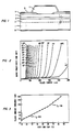
- FIG. 1 An end view of a ridge waveguide laser fabricated according to the present invention is depicted in Fig. 1.
- the device comprises substrate 1 having a first conductivity type, a first cladding layer 3, active layer 5, second cladding layer 7, dielectric layer 9, semiconductor ridge 11, and metallization layers 13 and 15.
- Metallization layers 13 and 15 contact the dielectric layer and ridge, and the substrate, respectively.
- the resulting ohmic contacts permit a forward bias voltage to be applied.
- the active layer emits radiation along the long axis of the active layer. There are thus electrical contacts to the ridge and the first cladding layer.
- the ridge contacts the second cladding layer 7 through a stripe opening in the dielectric layer.
- the ridge need not contact the second cladding layer as intermediate layers may be present.
- the first and second cladding layers have first and second conductivity types, respectively.
- the ridge has the second conductivity type.
- the active layer 5 may have either conductivity type.
- the substrate, cladding layers and ridge comprise semiconductors such as Group III-V or Group II-VI compound semiconductors.
- the cladding layers may comprise InP and the active layer may comprise a quaternary such as InGaAsP.
- the cladding layers may comprise one InGaAsP alloy composition and the active layer may comprise another JnGaAsP alloy composition having a narrower bandgap than do the cladding layers.
- the first and second cladding layers have first and second bandgaps, respectively, and the active layer has a third bandgap which is smaller than the first or second bandgap.
- the cladding layers and ridge, i.e., the epitaxial layers, are at least approxmately lattice matched to the substrate.
- the dielectric layer may comprise an oxide such as silicon dioxide or other dielectrics such as silicon nitride.
- the structure may be fabricated by the following method.
- the epitaxial layers, except the ridge layer, are epitaxially grown in a well-known manner on the substrate.
- An insulating film of, for example, Si0 2 or Si 3 N 4 is then deposited by, for example, chemical vapor deposition on the exposed surface of the second cladding layer.
- a window stripe is then etched through the dielectric layer to expose the surface of the second cladding layer.
- the structure is then reintroduced into the crystal growth apparatus, such as a liquid phase epitaxy reactor or vapor phase epitaxy reactor, for growth of the ridge in the window stripe. No growth occurs on the oxide mask, thus resulting in an oxide restricted ridge waveguide structure.
- a thicker ridge is obtained, as shown in Fig. 1, with lateral overgrowth extending beyond the window stripe and over the dielectric layer along the stripe edges. Finally, the entire top surface is metallized as is the exposed substrate surface. It should be noted that the top metallization automatically results in current injection confinement to the ridge overgrowth structure.
- the first and second conductivity types were n-type and p-type, respectively.
- the dielectric layer comprised a 0.15 ⁇ m thick layer of Si0 2 and the window stripe was 5 ⁇ m wide.
- Lateral growth of the ridge extends over the oxide film restricting the dimensions of the window stripe.
- the extent of lateral growth appears symmetric on both sides of the ridge and is in intimate contact with the oxide surface.
- the thickness of the oxide film is tapered, as shown in Fig. 1, near the edges, i.e., near the ridge, because the window stripe is formed by chemical etching.
- These characteristics loosen the lateral confinement of the optical field which extends beyond the window stripe into a portion of the second cladding layer underneath the oxide layer. This results in a narrower lateral beam divergence for the same window stripe width than would result if the optical field were more tightly confined.
- the lateral evanescent field does not suffer optical absorption by the metal film on top of the oxide film as it does for conventional etched ridge waveguide lasers with a thin oxide film.
- the ohmic contact is formed over all the exposed surfaces of the grown ridge, and that all of the injected current passes through only the narrow window stripe. As a result, the current density at the semiconductor-metal interface is greatly reduced. Furthermore, surface current leakage may be reduced as the surfaces are as grown rather than etched.
- the surface of the structure, except for the narrow window stripe, is covered with an oxide film when growth of the ridge begins.
- the rate of material deposition in the stripe is very rapid when growth begins.
- a ridge thickness of 3 ⁇ m was grown in 5 seconds with a growth temperature of 600 degrees C and a cooling rate of 2 degrees C/sec. These conditions result in a very uniform ridge overgrowth which is independent of the orientation of the window stripe along the (110) or (110) direction. It is noted that those growth conditions also result in negligible meltback of the InGaAsP material in the window stripe.
- Fig. 2 plots the light-current characteristics of a typical laser according to our invention for several operating temperatures.
- the output power per facet in arbitrary units is plotted vertically versus the pulsed current in units of mA plotted horizontally.
- the operating temperatures in units of degrees C are shown for each curve.
- the laser had a 1.5 ⁇ m InGaAsP active layer. Output powers as high as 50 mW/facet were obtained and the external differential quantum efficiencies from both facets were approximately 25 to 35 percent.
- the lowest current threshold for lasers with a 5 pm stripe and a 250 pm long cavity was 70 mA. Very stable far field patterns were obtained. At powers up to approximately 30 mW/facet, the half power at full width beam divergence was approximately 12 degrees. It should be noted that this value is smaller than those obtained with etched ridge waveguide lasers.
- Fig. 3 plots the heat sink temperature horizontally in units of degrees C versus the threshold current vertically in units of mA. A temperature coefficient, To, of 45 degrees K was obtained for low heat sink temperatures.
- the second cladding layer further comprises a distributed feedback grating 17 comprising a plurality of grooves with the grooves running in a direction perpendicular to the longitudinal dimension of the ridge. As is evident, the oxide layer conforms to the grooves.
- the semiconductor surface is conveniently corrugated, that is, the grooves are fabricated and the grating formed, after the first epilayer growth cycle, i.e., after the second cladding layer has been grown.
- room temperature photoluminescence and layer thickness measurements are conveniently used to determine the required grating period at this point in the fabrication sequence.
- the ability to determine the grating period after the initial layered structure has been grown is desirable because the appropriate grating period for the distributed feedback laser may be precisely determined and fabricated. Photolithography and chemical etching may be used to form the grooves.
- the direction of the grooves was ⁇ 110>.
- the dielectric layer is deposited and window stripes etched to the surface of the second cladding layer.
- An exemplary value for the dielectric layer thickness is 0.15 pm.
- the structure is then reintroduced into the liquid phase epitaxy or vapor phase epitaxy reactor for overgrowth of the ridge.
- the lateral overgrowth described appears particularly important in a DFB laser.
- the extent of the lateral growth is symmetric on both sides of the stripe and is in contact with the oxide surface.
- the lateral optical confinement extends into the grating periods under the oxide layer and results in increased distributed feedback because of the lateral evanescent field as well as narrower lateral beam divergence.
- the overgrowth over the oxide also increases the evanescent field intensity at the grating-oxide interface and results in a stronger electric field interaction with the grating.
- the oxide has an index of refraction of approximately 1.45 and the insertion of the oxide between the overgrowth and the corrugated surface increases the grating effect, or coupling coefficient, of the lateral evanescent field gratings. It is additionally noted that the presence of the oxide spacer layer in the evanescent electric field regions should significantly increase mode discrimination thus leading to stronger single longitudinal mode operation when even order gratings are used.
- Fig. 5 plots the pulsed current horizontally in units of mA versus the output power vertically in arbitrary units for a DFB laser.
- the heat sink temperature increases by 5 degrees C between curves with the left and right curves being at temperatures of 10 and 75 degrees C, respectively.
- the heat sink temperature is plotted horizontally in units of degrees C versus the threshold current in units of mA vertically in Fig. 6.
- Single longitudinal mode operation was obtained over this entire temperature range.
- the secondary mode suppression ratios did vary.
- a well-behaved temperature coefficient, To of 63 degrees K was obtained.
- Pulsed spectra taken at different temperatures between 30 and 55 degrees C illustrated that the DFB laser operated in the same single longitudinal mode although the lasing wavelength increased by approximately 0.06 nm/degrees C.
- the spectra are plotted in Fig. 7 for heat sink temperatures of 30, 35, 40, 45, 50 and 55 degrees C.
- the variation in lasing wavelength as a function of heat sink temperature is depicted in Fig. 8.
- the heat sink temperature is plotted horizontally in units of degrees C versus the lasing wavelength vertically in units of nm.
- Pulsed spectra are plotted in Fig. 9 for output power levels of 0.3, 1.0, 3.0 and 5.0 mW. As is evident, the output is a single longitudinal mode centered at approximately 1.485 pm. Stable single longitudinal mode output was maintained up to a power level of typically approximately 8 mW/ facet. However, at higher powers, the intensity of the unwanted secondary modes became significant. It should be pointed out however that these measurements were made without the use of an anti-reflection coating on the facet. With an anti-reflection coating, the single mode output power typically can be doubled and the ratio of the primary to secondary mode intensities also increased.
Landscapes
- Physics & Mathematics (AREA)
- Geometry (AREA)
- Condensed Matter Physics & Semiconductors (AREA)
- General Physics & Mathematics (AREA)
- Electromagnetism (AREA)
- Optics & Photonics (AREA)
- Semiconductor Lasers (AREA)
Abstract
Claims (10)
Applications Claiming Priority (4)
| Application Number | Priority Date | Filing Date | Title |
|---|---|---|---|
| US06/613,468 US4575919A (en) | 1984-05-24 | 1984-05-24 | Method of making heteroepitaxial ridge overgrown laser |
| US613468 | 1984-05-24 | ||
| US06/613,469 US4622673A (en) | 1984-05-24 | 1984-05-24 | Heteroepitaxial ridge overgrown laser |
| US613469 | 1984-05-24 |
Publications (2)
| Publication Number | Publication Date |
|---|---|
| EP0182903A1 EP0182903A1 (fr) | 1986-06-04 |
| EP0182903B1 true EP0182903B1 (fr) | 1989-08-09 |
Family
ID=27087036
Family Applications (1)
| Application Number | Title | Priority Date | Filing Date |
|---|---|---|---|
| EP85903454A Expired EP0182903B1 (fr) | 1984-05-24 | 1985-04-22 | Procede de fabrication d'un laser a supercroissance d'arete heteroepitaxiale |
Country Status (3)
| Country | Link |
|---|---|
| EP (1) | EP0182903B1 (fr) |
| DE (1) | DE3572266D1 (fr) |
| WO (1) | WO1985005504A1 (fr) |
Families Citing this family (2)
| Publication number | Priority date | Publication date | Assignee | Title |
|---|---|---|---|---|
| DE3809609A1 (de) * | 1988-03-22 | 1989-10-05 | Siemens Ag | Laserdiode zur erzeugung streng monochromatischer laserstrahlung |
| JP2754957B2 (ja) * | 1991-07-10 | 1998-05-20 | 日本電気株式会社 | 半導体光制御素子およびその製造方法 |
Family Cites Families (2)
| Publication number | Priority date | Publication date | Assignee | Title |
|---|---|---|---|---|
| US3865646A (en) * | 1972-09-25 | 1975-02-11 | Bell Telephone Labor Inc | Dielectric optical waveguides and technique for fabricating same |
| US4400813A (en) * | 1981-07-20 | 1983-08-23 | Bell Telephone Laboratories, Incorporated | Crenelated-ridge waveguide laser |
-
1985
- 1985-04-22 EP EP85903454A patent/EP0182903B1/fr not_active Expired
- 1985-04-22 WO PCT/US1985/000744 patent/WO1985005504A1/fr not_active Ceased
- 1985-04-22 DE DE8585903454T patent/DE3572266D1/de not_active Expired
Non-Patent Citations (2)
| Title |
|---|
| Applied Physics Letters, vol. 37, no. 11, 1 December 1980, New York (US), J. Katz et al.: "Single-growth embedded epitaxy A1GaAs injection lasers with extremely low threshold currents", pp. 987-989 * |
| Applied Physics Letters, vol. 45, no. 12, 15 December 1984, New York, (US), W.T. Tsang et al.: "Heteroepitaxial ridge-overgrown distributed feedback laser at 1,5um", pp. 1272-1274 * |
Also Published As
| Publication number | Publication date |
|---|---|
| EP0182903A1 (fr) | 1986-06-04 |
| WO1985005504A1 (fr) | 1985-12-05 |
| DE3572266D1 (en) | 1989-09-14 |
Similar Documents
| Publication | Publication Date | Title |
|---|---|---|
| US4575919A (en) | Method of making heteroepitaxial ridge overgrown laser | |
| US3978426A (en) | Heterostructure devices including tapered optical couplers | |
| EP0356190A2 (fr) | Procédé de fabrication pour circuits intégrés photoniques | |
| EP0836255A1 (fr) | Réseau laser à diode et méthode de fabrication | |
| US5289484A (en) | Laser diode | |
| Westbrook et al. | Continuous-wave operation of 1.5 μm distributed-feedback ridge-waveguide lasers | |
| US4622673A (en) | Heteroepitaxial ridge overgrown laser | |
| EP0014588B1 (fr) | Dispositif semiconducteur émetteur de lumière | |
| US5580818A (en) | Fabrication process for semiconductor optical device | |
| Kobayashi et al. | High light output-power single-longitudinal-mode semiconductor laser diodes | |
| Razeghi et al. | cw operation of 1.57‐μm Ga x In1− x As y P1− y InP distributed feedback lasers grown by low‐pressure metalorganic chemical vapor deposition | |
| US20050185689A1 (en) | Optoelectronic device having a Discrete Bragg Reflector and an electro-absorption modulator | |
| Ougazzaden et al. | Atmospheric pressure MOVPE growth of high performance polarisation insensitive strain compensated MQW InGaAsP/InGaAs optical amplifier | |
| Tsang et al. | The heteroepitaxial ridge-overgrown distributed feedback laser | |
| Oohashi et al. | Reliability of 1300-nm spot-size converter integrated laser diodes for low-cost optical modules in access networks | |
| US5436924A (en) | Semiconductor laser device | |
| EP4122062A1 (fr) | Laser modulé par électroabsorption | |
| Broberg et al. | 1.54‐μm phase‐adjusted InGaAsP/InP distributed feedback lasers with mass‐transported windows | |
| Saul et al. | Light-emitting-diode device design | |
| Lindström et al. | One watt CW visible single-quantum-well lasers | |
| Bornholdt et al. | Passive optical GaInAsP/InP waveguides | |
| US4627065A (en) | Double active layer semiconductor laser | |
| Savolainen et al. | AlGaInAs/InP strained-layer quantum well lasers at 1.3 µm grown by solid source molecular beam epitaxy | |
| WO1985005504A1 (fr) | Procede de fabrication d'un laser a supercroissance d'arete heteroepitaxiale | |
| Botez | Single-mode AlGaAs diode lasers |
Legal Events
| Date | Code | Title | Description |
|---|---|---|---|
| PUAI | Public reference made under article 153(3) epc to a published international application that has entered the european phase |
Free format text: ORIGINAL CODE: 0009012 |
|
| AK | Designated contracting states |
Kind code of ref document: A1 Designated state(s): BE DE FR GB IT NL SE |
|
| 17P | Request for examination filed |
Effective date: 19860509 |
|
| 17Q | First examination report despatched |
Effective date: 19870803 |
|
| GRAA | (expected) grant |
Free format text: ORIGINAL CODE: 0009210 |
|
| AK | Designated contracting states |
Kind code of ref document: B1 Designated state(s): BE DE FR GB IT NL SE |
|
| ITF | It: translation for a ep patent filed | ||
| REF | Corresponds to: |
Ref document number: 3572266 Country of ref document: DE Date of ref document: 19890914 |
|
| ET | Fr: translation filed | ||
| PLBE | No opposition filed within time limit |
Free format text: ORIGINAL CODE: 0009261 |
|
| STAA | Information on the status of an ep patent application or granted ep patent |
Free format text: STATUS: NO OPPOSITION FILED WITHIN TIME LIMIT |
|
| 26N | No opposition filed | ||
| ITTA | It: last paid annual fee | ||
| PGFP | Annual fee paid to national office [announced via postgrant information from national office to epo] |
Ref country code: BE Payment date: 19930301 Year of fee payment: 9 |
|
| PGFP | Annual fee paid to national office [announced via postgrant information from national office to epo] |
Ref country code: SE Payment date: 19930413 Year of fee payment: 9 |
|
| PGFP | Annual fee paid to national office [announced via postgrant information from national office to epo] |
Ref country code: NL Payment date: 19930430 Year of fee payment: 9 |
|
| PG25 | Lapsed in a contracting state [announced via postgrant information from national office to epo] |
Ref country code: SE Effective date: 19940423 |
|
| PG25 | Lapsed in a contracting state [announced via postgrant information from national office to epo] |
Ref country code: BE Effective date: 19940430 |
|
| BERE | Be: lapsed |
Owner name: AMERICAN TELEPHONE AND TELEGRAPH CY Effective date: 19940430 |
|
| PG25 | Lapsed in a contracting state [announced via postgrant information from national office to epo] |
Ref country code: NL Effective date: 19941101 |
|
| NLV4 | Nl: lapsed or anulled due to non-payment of the annual fee | ||
| EUG | Se: european patent has lapsed |
Ref document number: 85903454.8 Effective date: 19941110 |
|
| PGFP | Annual fee paid to national office [announced via postgrant information from national office to epo] |
Ref country code: FR Payment date: 20000322 Year of fee payment: 16 |
|
| PGFP | Annual fee paid to national office [announced via postgrant information from national office to epo] |
Ref country code: GB Payment date: 20000327 Year of fee payment: 16 |
|
| PG25 | Lapsed in a contracting state [announced via postgrant information from national office to epo] |
Ref country code: GB Free format text: LAPSE BECAUSE OF NON-PAYMENT OF DUE FEES Effective date: 20010422 |
|
| PG25 | Lapsed in a contracting state [announced via postgrant information from national office to epo] |
Ref country code: FR Free format text: THE PATENT HAS BEEN ANNULLED BY A DECISION OF A NATIONAL AUTHORITY Effective date: 20010430 |
|
| PGFP | Annual fee paid to national office [announced via postgrant information from national office to epo] |
Ref country code: DE Payment date: 20010629 Year of fee payment: 17 |
|
| GBPC | Gb: european patent ceased through non-payment of renewal fee |
Effective date: 20010422 |
|
| REG | Reference to a national code |
Ref country code: FR Ref legal event code: ST |
|
| PG25 | Lapsed in a contracting state [announced via postgrant information from national office to epo] |
Ref country code: DE Free format text: LAPSE BECAUSE OF NON-PAYMENT OF DUE FEES Effective date: 20021101 |