EP0182913A1 - Procede de reglage de circuits electroniques - Google Patents
Procede de reglage de circuits electroniques Download PDFInfo
- Publication number
- EP0182913A1 EP0182913A1 EP85902163A EP85902163A EP0182913A1 EP 0182913 A1 EP0182913 A1 EP 0182913A1 EP 85902163 A EP85902163 A EP 85902163A EP 85902163 A EP85902163 A EP 85902163A EP 0182913 A1 EP0182913 A1 EP 0182913A1
- Authority
- EP
- European Patent Office
- Prior art keywords
- adjusting
- electronic circuit
- melt
- current
- cut
- Prior art date
- Legal status (The legal status is an assumption and is not a legal conclusion. Google has not performed a legal analysis and makes no representation as to the accuracy of the status listed.)
- Granted
Links
Images

Classifications
-
- H—ELECTRICITY
- H03—ELECTRONIC CIRCUITRY
- H03H—IMPEDANCE NETWORKS, e.g. RESONANT CIRCUITS; RESONATORS
- H03H1/00—Constructional details of impedance networks whose electrical mode of operation is not specified or applicable to more than one type of network
-
- H—ELECTRICITY
- H04—ELECTRIC COMMUNICATION TECHNIQUE
- H04N—PICTORIAL COMMUNICATION, e.g. TELEVISION
- H04N17/00—Diagnosis, testing or measuring for television systems or their details
- H04N17/04—Diagnosis, testing or measuring for television systems or their details for receivers
Definitions
- This invention relates to a method for adjusting an electronic circuit used for a television receiver or the like when it is adjusted upon being manufactured.
- the characteristic thereof is normally changed and adjusted by finely adjusting a magnitude of a current flowing through such circuit.
- the electronic circuit is set in the driving (operating) mode and under this state, by rotating a semi-fixed resistor inserted into the circuit, the voltage and the like at a necessary operation point are adjusted so as to be fallen within a standardized value.
- the scattering of the semi-fixed resistor itself is large, even if the adjusting angle of the semi-fixed resistor is determined, the characteristics of all the electronic circuits can not always fall within the standardized values. For this reason, the rotational adjustment must be carried out in each electronic circuit, requiring a relatively long time of about 20 seconds for one adjustment. Further, since the semi-fixed resistor is of a so-called movable type, after the adjustment, the rotational angle may be changed due to the vibration, contact and so on. Accordingly, upon transportion and the like thereof, there is such a defect to pay a notice that this semi-fixed resistor is not touched, etc.
- this invention is to omit the semi-fixed resistor to thereby improve the reliability of the electronic circuit after it was adjusted and also is to simplify the adjustment itself to thereby reduce the adjusting time.
- a connection line which can be melt-cut by flowing a current thereto from the outside, is connected in series or in parallel to an adjusting element inserted into a predetermined current path within an electronic circuit; under a predetermined driving state of the electronic circuit, the operation state of this electronic circuit is detected by a detector circuit; on the basis of the detected result, it is judged whether the connection line is melt-cut or not; under the necessary state, the current is supplied to the connection wire from the outside to melt-cut the same; and a semi-fixed resistor is omitted, whereby the reliability after the adjustment is improved and also the adjustment itself is simplified, thus reducing the adjusting time.
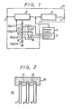
- Fig. 1 is a block diagram useful for explaining an embodiment of a method for adjusting an electronic circuit according to the present invention
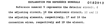
- Fig. 2 is a cross-sectional view illustrating an example of an element used in the present invention
- Figs. 3, 4, 5 and 6 are cross-sectional views illustrating main parts of other embodiments of the present invention, respectively.
- reference numeral 1 designates a signal input terminal, 2 a preceding stage circuit, 3 a succeeding stage circuit and 4 a signal output terminal.
- a DC power source such as a drive power supply source and the like in the preceding stage circuit 2
- four resistors 11, 12, 13 and 14 are connected in series.
- the connection point between the resistors 12 and 13 is connected to a predetermined point of the preceding stage circuit 2.
- the resistors 12 and 13 become adjusting elements and the resistance values thereof are selected to be extremely low as compared with other resistors 11 and 14.
- respective resistance values R l , R 2 , R 3 and R 4 of the resistors 11, 12, 13 and 14 are 200K ⁇ , 200 ⁇ , 300n and 300K ⁇ , respectively.
- An electronic circuit 10 is constructed as described above.
- the connection points among the respective resistors are denoted by P, Q and R, respectively.
- connection wires 17 and 18 are previously connected in parallel to the resistors 12 and 13 which become the adjusting elements, respectively.
- Fig. 2 illustrates an element 19 which incorporates therein the connection wires 17 and 18.
- the connection wires 17 and 18 are connected between one ends of three terminals 7, 8 and 9 made of conductive material and this portion is molded by a mold material 20 such as resin and so on.
- a mold material 20 such as resin and so on.
- connection wires 17 and 18 there can be used such one which can easliy be melt-cut by the current flowed thereto.
- such a connection . wire is suitable which can easily be melt-cut by a current of 2A (about 0.6V) for a time period of 2m sec.
- a detector circuit 5 As shown in Fig. 1, there are prepared a detector circuit 5 and an adjusting circuit 6. A measuring terminal (electrode) of the detector circuit 5 is connected to a necessary point to be measured (the connection point between the preceding stage circuit 2 and the succeeding stage circuit 3, in this embodiment) of the electronic circuit 10 and lead wires from the adjusting circuit 6 are respectively connected to the aforesaid points P, Q and R.
- the electronic circuit 10 is set in the driving (operating) state and the operating state (characteristic and the like) of the electronic circuit 10 is checked by the detector circuit 5. If the electronic circuit is in its normal operating state, the connection wires 17 and 18 are not melt-cut but are left as they are. Therefore, at that time, the resistors 12 and 13 are in the short-circuited state, respectively.
- connection wire 17 is melt-cut.
- both the resistors 12 and 13 are used is better, it is enough to melt-cut both the connection wires 17 and 18.
- While the supply of the current from the adjusting circuit 6 may be manually carried out on the basis of the detected result by the detector circuit 5, it may be possible that the supply of the current is automatically carried out by controlling the adjusting circuit 6 on the basis of a command signal issued from the detector circuit 5.
- the semi-fixed resistor tends to easily vary its resistance value due to the invasion of dusts, water and so on or because it has a movable portion, according to the method of the present invention, since such semi-fixed resistor is not required, even after it was adjusted, the resistance value thereof is not changed, thus increasing the reliability by that much.
- Fig. 3 illustrates other embodiment of the present invention.
- the resistor 13 as the adjusting element is connected in series to the connection wire 18
- other circuit elements are connected in the same way as those of Fig. 1.
- the respective resistance values R 1 , R 2 , R 3 and R 4 of the resistors 11, 12, 13 and 14 are selected to be 50K ⁇ ,270 ⁇ , 33K ⁇ and 4.7K ⁇ , respectively.
- the resistor 12 under the illustrated state, the resistor 12 is short-circuited and the resistors 14 and 13 are connected in parallel to each other, so that the resistance value between the points P and Q is zero and that the resistance value between the points Q and R is 41140 which is slightly lower than 4700Q. If under such state either the connection wire 17 or 18 or both of them are melt-cut the respective resistance values to the ground side and to the opposite side from the point Q can be adjusted finely.
- Fig. 4 shows a further embodiment of the present invention.
- two routes are provided for the P-Q-R path and the above mentioned connection wires 17 and 18 are interposed in the routes, in which the two routes are both used or either of them is used, selectively.
- Fig. 5 shows a further embodiment in which capacitors 22 and 23 as the adjusting elements are connected in parallel to a capacitor 21 via the connection wires 17 and 18.
- the capacity value can be adjusted by melt-cutting the connection wires 17 and 18 in the manner similar to the above.
- Fig. 6 shows a further embodiment in which coils 25 and 26 as the adjusting elements are connected in parallel to a coil 24 via the connection wires 17 and 18. Also in Fig. 6, the inductance value can be adjusted by melt-cutting the connection wires 17 and 18 similarly as described above.
- connection wire used for the interconnection of a semiconductor
- the adjusting element is provided in parallel to this bonding wire, they are molded integrally and terminals are led out from one and another ends of the molded member.
- connecting wires 17 and 18 are molded by the mold material, of course, they may be connected discretely.
Landscapes
- Engineering & Computer Science (AREA)
- Health & Medical Sciences (AREA)
- Biomedical Technology (AREA)
- General Health & Medical Sciences (AREA)
- Multimedia (AREA)
- Signal Processing (AREA)
- Apparatuses And Processes For Manufacturing Resistors (AREA)
- Testing, Inspecting, Measuring Of Stereoscopic Televisions And Televisions (AREA)
- Electric Clocks (AREA)
- Oscillators With Electromechanical Resonators (AREA)
- Details Of Television Systems (AREA)
- Semiconductor Integrated Circuits (AREA)
- Thermistors And Varistors (AREA)
- Filters And Equalizers (AREA)
Abstract
Priority Applications (1)
| Application Number | Priority Date | Filing Date | Title |
|---|---|---|---|
| AT85902163T ATE98825T1 (de) | 1984-05-10 | 1985-05-09 | Verfahren zum einstellen elektronischer schaltungen. |
Applications Claiming Priority (2)
| Application Number | Priority Date | Filing Date | Title |
|---|---|---|---|
| JP93729/84 | 1984-05-10 | ||
| JP59093729A JPS60236585A (ja) | 1984-05-10 | 1984-05-10 | 電子回路の調整方法 |
Publications (3)
| Publication Number | Publication Date |
|---|---|
| EP0182913A1 true EP0182913A1 (fr) | 1986-06-04 |
| EP0182913A4 EP0182913A4 (fr) | 1988-01-28 |
| EP0182913B1 EP0182913B1 (fr) | 1993-12-15 |
Family
ID=14090496
Family Applications (1)
| Application Number | Title | Priority Date | Filing Date |
|---|---|---|---|
| EP85902163A Expired - Lifetime EP0182913B1 (fr) | 1984-05-10 | 1985-05-09 | Procede de reglage de circuits electroniques |
Country Status (7)
| Country | Link |
|---|---|
| US (1) | US4689550A (fr) |
| EP (1) | EP0182913B1 (fr) |
| JP (1) | JPS60236585A (fr) |
| KR (1) | KR860700191A (fr) |
| AT (1) | ATE98825T1 (fr) |
| DE (1) | DE3587686T2 (fr) |
| WO (1) | WO1985005510A1 (fr) |
Families Citing this family (11)
| Publication number | Priority date | Publication date | Assignee | Title |
|---|---|---|---|---|
| JP2577897B2 (ja) * | 1986-10-31 | 1997-02-05 | 日本テキサス・インスツルメンツ 株式会社 | 定電圧電源回路 |
| US4978904A (en) * | 1987-12-15 | 1990-12-18 | Gazelle Microcircuits, Inc. | Circuit for generating reference voltage and reference current |
| US4970415A (en) * | 1989-07-18 | 1990-11-13 | Gazelle Microcircuits, Inc. | Circuit for generating reference voltages and reference currents |
| JP2601933B2 (ja) * | 1990-04-13 | 1997-04-23 | 株式会社東芝 | 固体撮像装置 |
| US5780918A (en) * | 1990-05-22 | 1998-07-14 | Seiko Epson Corporation | Semiconductor integrated circuit device having a programmable adjusting element in the form of a fuse mounted on a margin of the device and a method of manufacturing the same |
| JPH04373148A (ja) * | 1991-06-21 | 1992-12-25 | Nippon Steel Corp | 半導体装置のヒューズ構造 |
| US5410186A (en) * | 1991-12-19 | 1995-04-25 | International Business Machines Company | Programmable digital to analog converter |
| US5367202A (en) * | 1992-11-06 | 1994-11-22 | National Semiconductor Corporation | Voltage reference ladder having improved linearity |
| JPH10135756A (ja) * | 1996-10-31 | 1998-05-22 | Mitsumi Electric Co Ltd | 回路体における回路特性の調整方法 |
| JP3398564B2 (ja) * | 1997-04-11 | 2003-04-21 | 富士通株式会社 | 半導体装置 |
| US6822345B2 (en) * | 2002-04-09 | 2004-11-23 | Sun Microsystems, Inc. | Chip/package resonance damping using controlled package series resistance |
Family Cites Families (7)
| Publication number | Priority date | Publication date | Assignee | Title |
|---|---|---|---|---|
| US3656115A (en) * | 1971-04-19 | 1972-04-11 | Bunker Ramo | Fusible link matrix for programmable networks |
| DE2256688B2 (de) * | 1972-11-18 | 1976-05-06 | Robert Bosch Gmbh, 7000 Stuttgart | Verfahren zum auftrennen von leiterbahnen auf integrierten schaltkreisen |
| US4016483A (en) * | 1974-06-27 | 1977-04-05 | Rudin Marvin B | Microminiature integrated circuit impedance device including weighted elements and contactless switching means for fixing the impedance at a preselected value |
| JPS529850A (en) * | 1975-07-15 | 1977-01-25 | Oki Electric Ind Co Ltd | Semiifixed electron variable resistor |
| US4150366A (en) * | 1976-09-01 | 1979-04-17 | Motorola, Inc. | Trim network for monolithic circuits and use in trimming a d/a converter |
| US4201970A (en) * | 1978-08-07 | 1980-05-06 | Rca Corporation | Method and apparatus for trimming resistors |
| US4412241A (en) * | 1980-11-21 | 1983-10-25 | National Semiconductor Corporation | Multiple trim structure |
-
1984
- 1984-05-10 JP JP59093729A patent/JPS60236585A/ja active Pending
-
1985
- 1985-05-09 WO PCT/JP1985/000261 patent/WO1985005510A1/fr not_active Ceased
- 1985-05-09 KR KR1019850700416A patent/KR860700191A/ko not_active Ceased
- 1985-05-09 DE DE85902163T patent/DE3587686T2/de not_active Expired - Fee Related
- 1985-05-09 AT AT85902163T patent/ATE98825T1/de not_active IP Right Cessation
- 1985-05-09 US US06/822,303 patent/US4689550A/en not_active Expired - Lifetime
- 1985-05-09 EP EP85902163A patent/EP0182913B1/fr not_active Expired - Lifetime
Also Published As
| Publication number | Publication date |
|---|---|
| EP0182913A4 (fr) | 1988-01-28 |
| DE3587686T2 (de) | 1994-04-07 |
| KR860700191A (ko) | 1986-03-31 |
| ATE98825T1 (de) | 1994-01-15 |
| WO1985005510A1 (fr) | 1985-12-05 |
| EP0182913B1 (fr) | 1993-12-15 |
| JPS60236585A (ja) | 1985-11-25 |
| US4689550A (en) | 1987-08-25 |
| DE3587686D1 (de) | 1994-01-27 |
Similar Documents
| Publication | Publication Date | Title |
|---|---|---|
| EP0182913A1 (fr) | Procede de reglage de circuits electroniques | |
| US6838891B2 (en) | Semiconductor device | |
| EP0720023B1 (fr) | Procédé de test pour éléments intégrés de puissance | |
| KR100502057B1 (ko) | 광전기 변환 집적회로장치 | |
| US4612453A (en) | Integrated circuit device having a circuit means for detecting a disconnection of input signal line | |
| JP3814019B2 (ja) | 半導体ic用のヒュージング回路 | |
| JPH06186254A (ja) | 電流検出用チップ形抵抗体 | |
| US4868640A (en) | Integrated optoelectronic circuit | |
| US4797578A (en) | Arrangement for adjusting an impedance network in an integrated semiconductor circuit | |
| FR2728117A1 (fr) | Circuit de commande pour interrupteur electronique et interrupteur en faisant application | |
| KR100326063B1 (ko) | 본딩 패드용 테스트 장치 | |
| US5101154A (en) | Open bond detector for an integrated circuit | |
| US6111758A (en) | Electronic component having alternate functionalities | |
| EP0167884A2 (fr) | Alimentation à tension continue avec une protection contre les surintensités de courant | |
| JP2003533048A (ja) | 半導体装置および半導体装置の製造方法 | |
| US5325071A (en) | Operational amplifier with digitally programmable gain circuitry on the same chip | |
| JP2824360B2 (ja) | 電流検出用半導体装置 | |
| JP2752432B2 (ja) | 電流センサ及びそれを使用した電流検知方法 | |
| KR870001820B1 (ko) | 단선지점 감지용 경보장치 | |
| JPH0716177B2 (ja) | 光送信回路 | |
| KR940002770Y1 (ko) | 반도체 소자의 저항 트리밍 장치 | |
| CA1118850A (fr) | Circuit d'entree pour systemes de controle numeriques | |
| JPS63308410A (ja) | 二端子網の光センサ | |
| JPH0521203A (ja) | 電子回路基板 | |
| KR850002431Y1 (ko) | 텔레비젼의 동조전압 자동 상승-하강회로 |
Legal Events
| Date | Code | Title | Description |
|---|---|---|---|
| PUAI | Public reference made under article 153(3) epc to a published international application that has entered the european phase |
Free format text: ORIGINAL CODE: 0009012 |
|
| 17P | Request for examination filed |
Effective date: 19860102 |
|
| AK | Designated contracting states |
Kind code of ref document: A1 Designated state(s): AT DE FR GB IT NL |
|
| A4 | Supplementary search report drawn up and despatched |
Effective date: 19880128 |
|
| 17Q | First examination report despatched |
Effective date: 19891208 |
|
| GRAA | (expected) grant |
Free format text: ORIGINAL CODE: 0009210 |
|
| AK | Designated contracting states |
Kind code of ref document: B1 Designated state(s): AT DE FR GB IT NL |
|
| REF | Corresponds to: |
Ref document number: 98825 Country of ref document: AT Date of ref document: 19940115 Kind code of ref document: T |
|
| REF | Corresponds to: |
Ref document number: 3587686 Country of ref document: DE Date of ref document: 19940127 |
|
| ITF | It: translation for a ep patent filed | ||
| ET | Fr: translation filed | ||
| ITTA | It: last paid annual fee | ||
| PLBE | No opposition filed within time limit |
Free format text: ORIGINAL CODE: 0009261 |
|
| STAA | Information on the status of an ep patent application or granted ep patent |
Free format text: STATUS: NO OPPOSITION FILED WITHIN TIME LIMIT |
|
| 26N | No opposition filed | ||
| PGFP | Annual fee paid to national office [announced via postgrant information from national office to epo] |
Ref country code: DE Payment date: 20010430 Year of fee payment: 17 |
|
| PGFP | Annual fee paid to national office [announced via postgrant information from national office to epo] |
Ref country code: GB Payment date: 20010509 Year of fee payment: 17 |
|
| PGFP | Annual fee paid to national office [announced via postgrant information from national office to epo] |
Ref country code: AT Payment date: 20010514 Year of fee payment: 17 |
|
| PGFP | Annual fee paid to national office [announced via postgrant information from national office to epo] |
Ref country code: FR Payment date: 20010518 Year of fee payment: 17 |
|
| PGFP | Annual fee paid to national office [announced via postgrant information from national office to epo] |
Ref country code: NL Payment date: 20010531 Year of fee payment: 17 |
|
| REG | Reference to a national code |
Ref country code: GB Ref legal event code: IF02 |
|
| PG25 | Lapsed in a contracting state [announced via postgrant information from national office to epo] |
Ref country code: GB Free format text: LAPSE BECAUSE OF NON-PAYMENT OF DUE FEES Effective date: 20020509 Ref country code: AT Free format text: LAPSE BECAUSE OF NON-PAYMENT OF DUE FEES Effective date: 20020509 |
|
| PG25 | Lapsed in a contracting state [announced via postgrant information from national office to epo] |
Ref country code: NL Free format text: LAPSE BECAUSE OF NON-PAYMENT OF DUE FEES Effective date: 20021201 |
|
| PG25 | Lapsed in a contracting state [announced via postgrant information from national office to epo] |
Ref country code: DE Free format text: LAPSE BECAUSE OF NON-PAYMENT OF DUE FEES Effective date: 20021203 |
|
| GBPC | Gb: european patent ceased through non-payment of renewal fee |
Effective date: 20020509 |
|
| PG25 | Lapsed in a contracting state [announced via postgrant information from national office to epo] |
Ref country code: FR Free format text: LAPSE BECAUSE OF NON-PAYMENT OF DUE FEES Effective date: 20030131 |
|
| NLV4 | Nl: lapsed or anulled due to non-payment of the annual fee |
Effective date: 20021201 |
|
| REG | Reference to a national code |
Ref country code: FR Ref legal event code: ST |